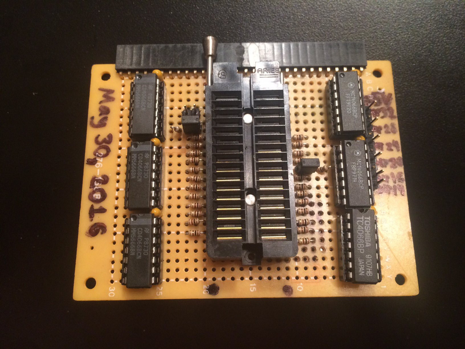
 SHAOS
SHAOSFor now assume that all tested ICs are having GND at the left-bottom pin (I know it is not always true, but we may add support of other classes of chips later), all ICs will be installed to the bottom of ZIF-socket and we may have DIP14, DIP16, DIP20, DIP24, DIP28 and DIP32, so optional VCC could optionally appear in 5 different places (and pin 32 will have VCC permanently):
| PIN# | ========= 32-pin ZIF-socket ========= | PIN# | ||
| 1 | VPP (opt) | DIP32 top (memory 512K or 128K) | VCC (permanent) | 32 |
| 2 | X7 (IO) | Y1 (I) | 31 | |
| 3 | X6 (IO, opt.VPP) | DIP28 top (memory 32K or 8K) | Y0 (I, opt.VCC) | 30 |
| 4 | X3 (IO) | R3.7 (IO) | 29 | |
| 5 | R2.7 (IO) | DIP24 top (memory 2K or any other IC) | R3.6 (IO, opt.VCC) | 28 |
| 6 | R2.6 (IO) | R3.5 (IO) | 27 | |
| 7 | R2.5 (IO) | DIP20 top (any IC) | R3.4 (IO, opt.VCC) | 26 |
| 8 | R2.4 (IO) | R3.3 (IO, opt.VPP) | 25 | |
| 9 | R2.3 (IO) | DIP16 top (any IC) | R3.2 (IO, opt.VCC) | 24 |
| 10 | R2.2 (IO) | DIP14 top (any IC) | R3.1 (IO, opt.VCC) | 23 |
| 11 | R2.1 (IO) | R3.0 (IO) | 22 | |
| 12 | R2.0 (IO) | R1.7 (IO) | 21 | |
| 13 | R1.0 (IO) | R1.6 (IO) | 20 | |
| 14 | R1.1 (IO) | R1.5 (IO) | 19 | |
| 15 | R1.2 (IO) | R1.4 (IO) | 18 | |
| 16 | GND (perm) | R1.3 (IO) | 17 |
As you can see we need at least 3 8-bit registers (R1,R2,R3) plus 5 additional bits to set remaining inputs of tested chip (Xn,Yn). Optional VCC could be handled manually by jumper switches...
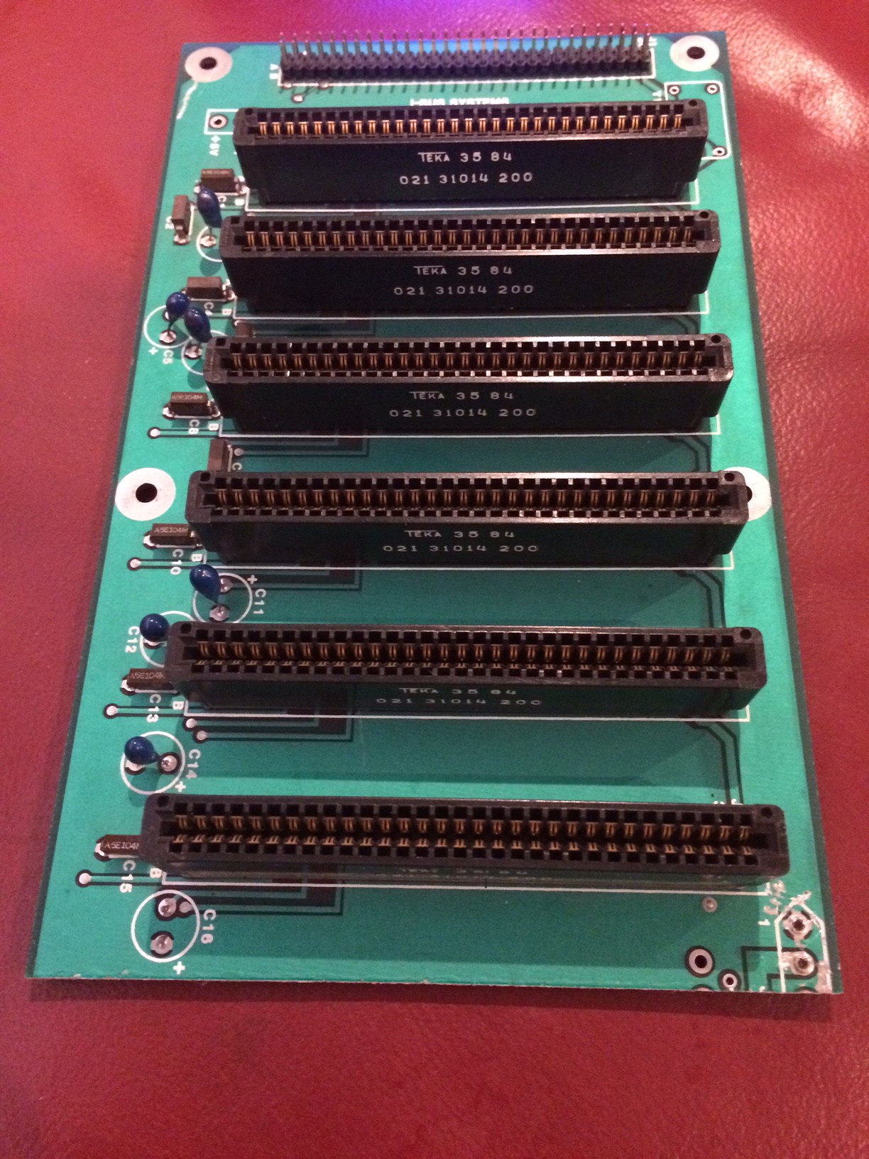
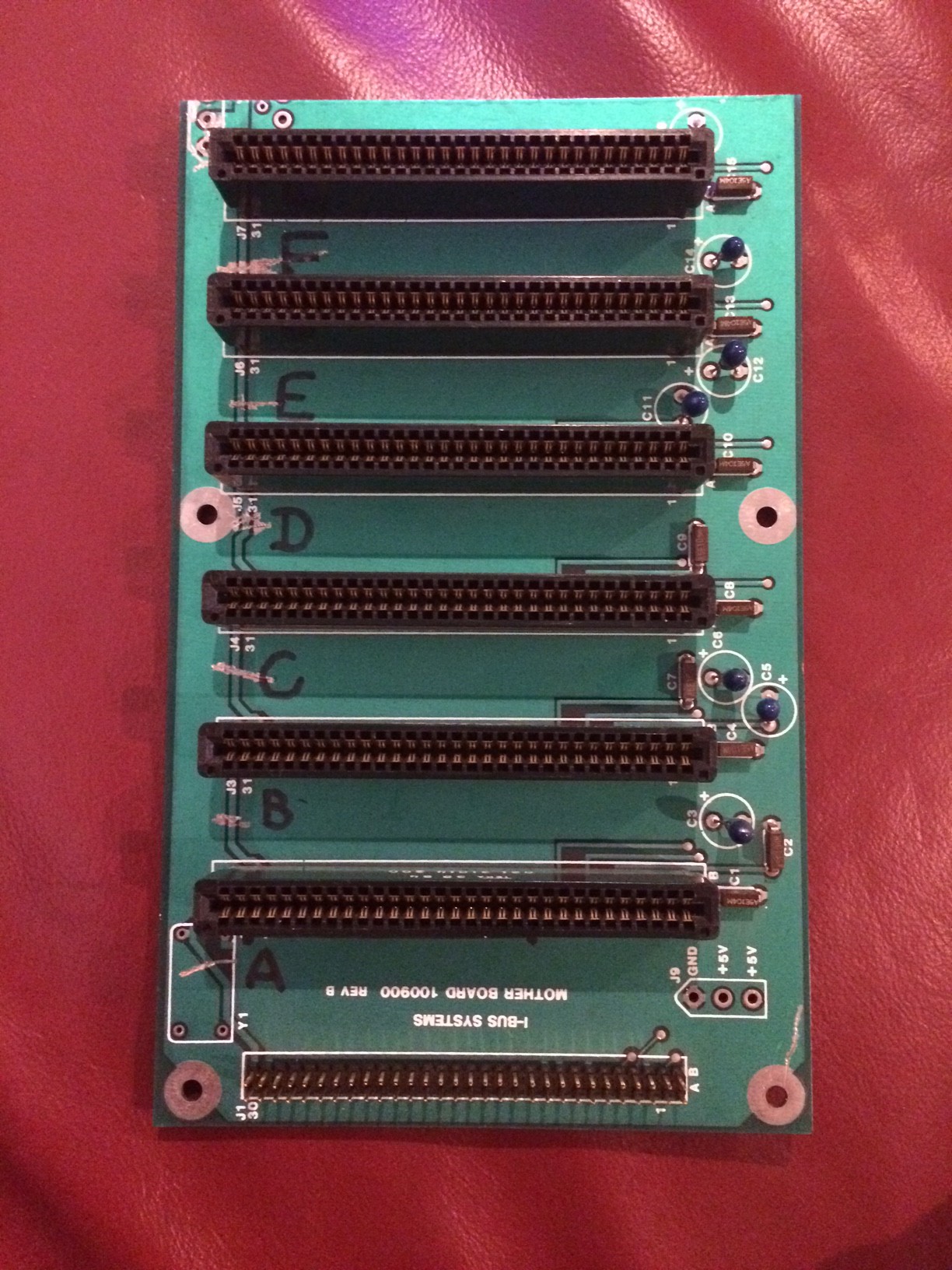
Also in parallel it may have header female receptacle with enough IO-pins to test any of NEDONAND modules :)
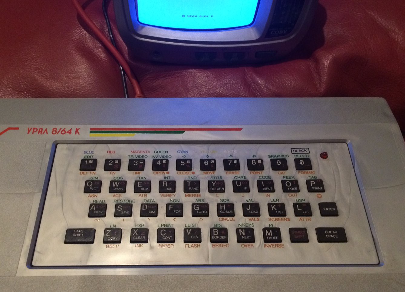
 Another problem was to find TV that could recognize PAL/SECAM timings and usually it's a lottery because TVs in US may officially do NTSC only and you need to try to make sure that it may or may not be adjusted to recognize different video system:
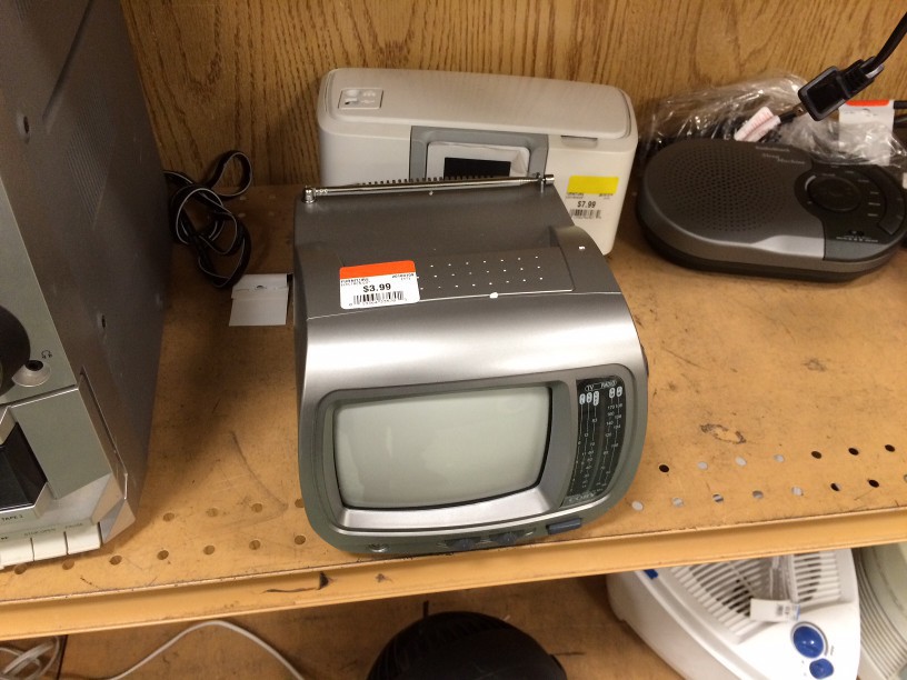


 jimshortz
 Keith
Keith
 forthnutter
 Emilio P.G. Ficara
> (it could NOT be PC at all)
But you just gave the pinout/capabilities of the PC's parallel printer port :-D