SHAOS
SHAOS-
Backplane
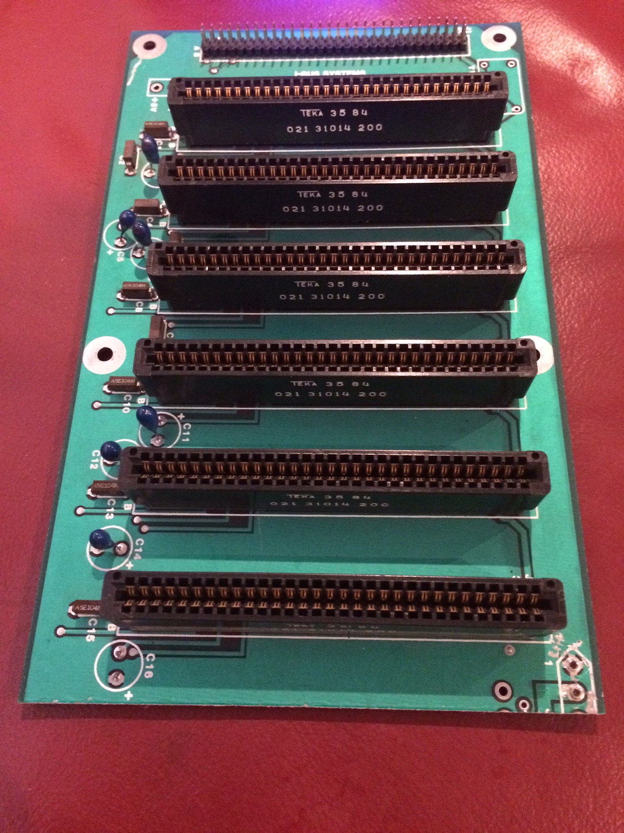
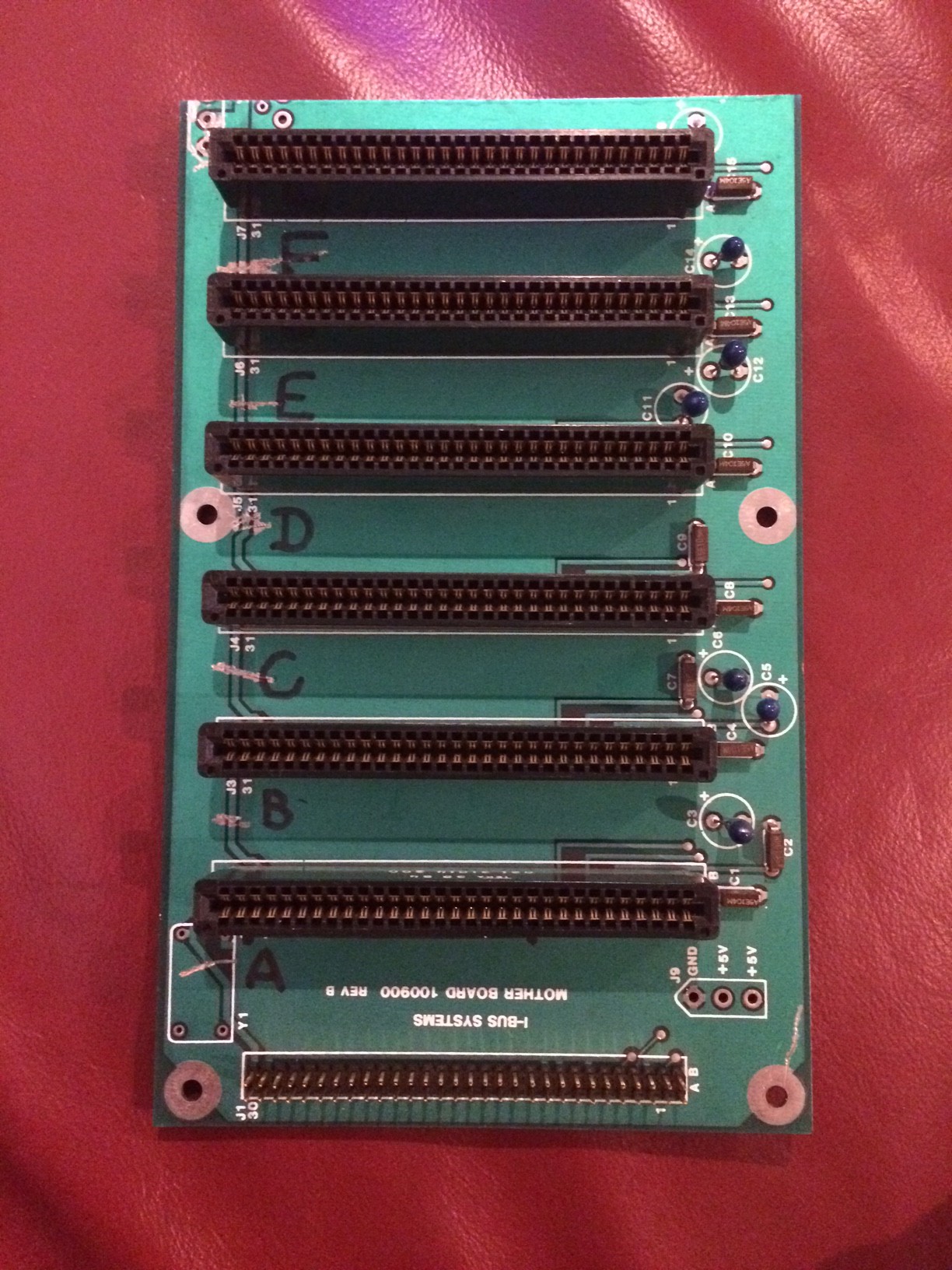
05/31/2016 at 04:57 • 0 commentsI decided that interface between ZIF-socket and host machine will be implemented with help of this antique ISA backplane manufactured in 1984 (I bought it for about $20 last month):
![]()
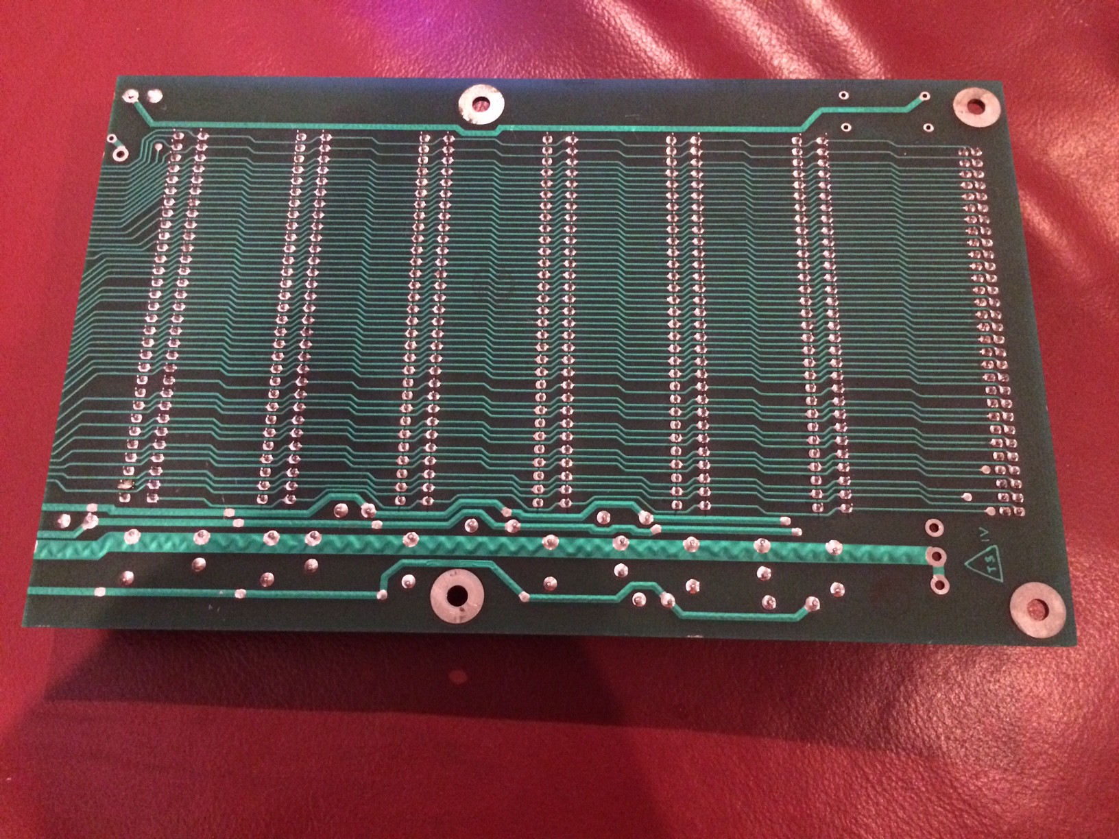
I cut out it a little to remove part with pull-up resistors, because it shortened power to the ground somewhere. On the back we can see all signals go through so technically this board could be easily used to implement any custom backplane solution:
![]()
For my task I will use part of upside-down ISA-socket where quasi-disks and peripherals (including tester/programmer) will be inserted:
![]()
I marked places A,B,C,D,E and F. Also I cut wire that was used as CLK in ISA - now it will be repurposed as individual /CS for every board. Pinout of the socket in this case uses only 42 contacts from socket and most of them repurposed, so it is NOT an ISA bus anymore (I only kept +5V, ground and partially address on their usual locations):
1 A0 GND 42 2 A1 /CS 41 3 A2 VCC 40 4 A3 X7 39 5 A4 X6 38 6 A5 X5 37 7 A6 X4 36 8 A7 X3 35 9 A8 A23 34 10 A9 A22 33 11 A10 A21 32 12 A11 D7 31 13 A12 D6 30 14 A13 D5 29 15 A14 D4 28 16 A15 D3 27 17 A16 D2 26 18 A17 D1 25 19 A18 D0 24 20 A19 /RD 23 21 A20 /WR 22 All signals are shared across all sockets except for /CS that individually wired to every slot (8 CS generated by X0,X1,X2 and that's why those 3 bits are not routed into the socket).
You can ask why tester needs quasi disk interface? I think it's cool when device may provide software to control itself right away - so ROM disk C may have a program with component library to run (I can do this program capable to work on many 8080 compatible machine, not only Soviet clones of ZX-Spectrum) and RAM disk A may be used to store test results...
-
Host Machine was Chosen
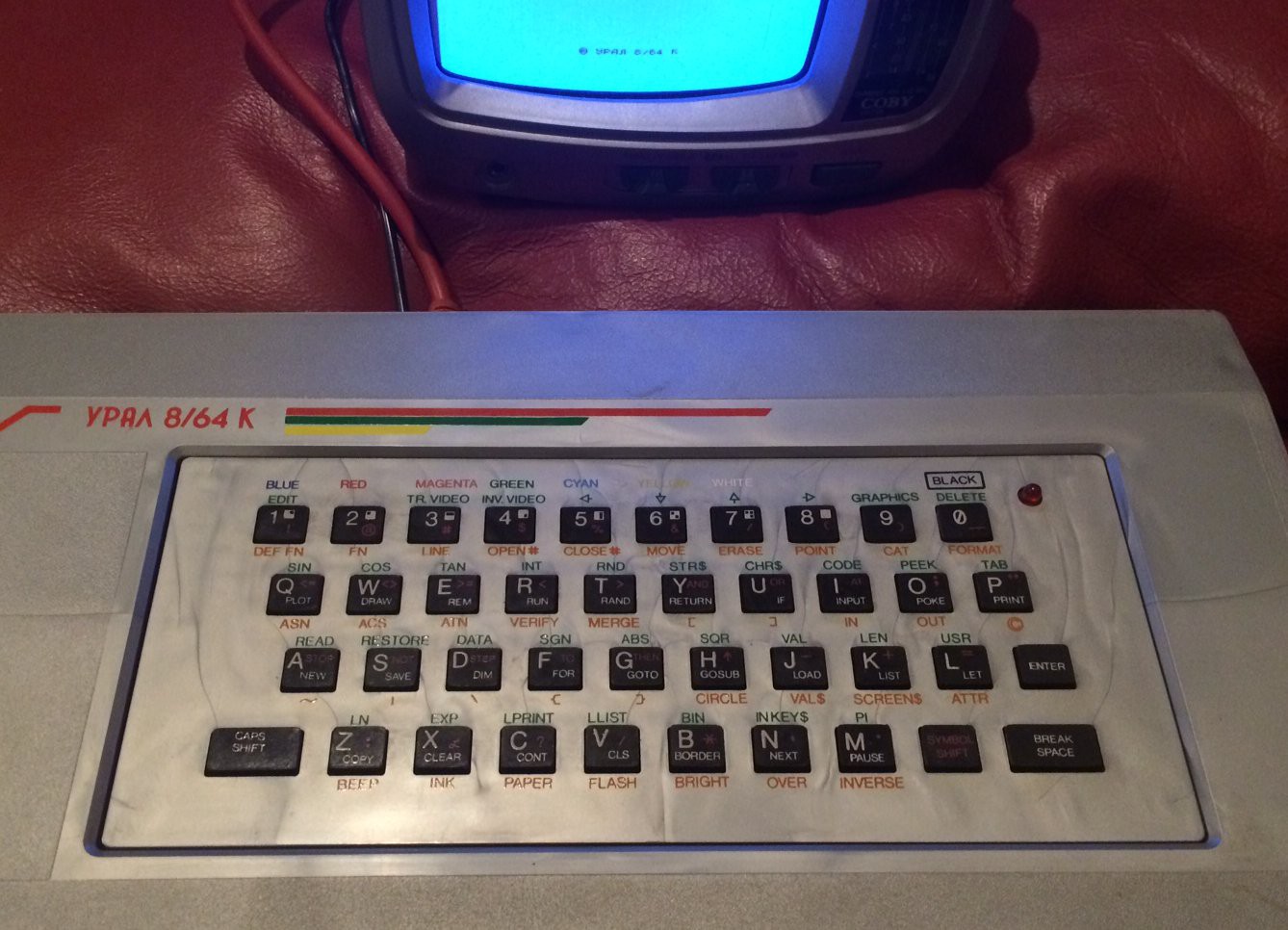
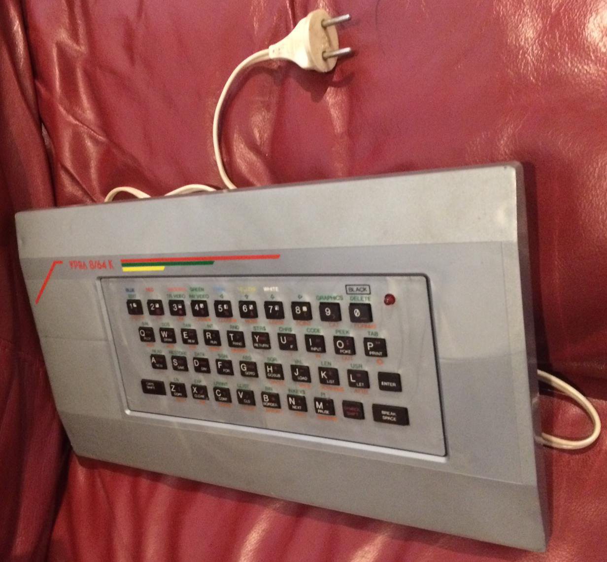
05/31/2016 at 03:57 • 0 commentsI think it's time to reveal the host machine that I will use to control the tester/programmer. As I mentioned in previous log, it will be some sort of interface that I designed in 90s for my home computer, but never actually built it in full. It was quasi-disk and other peripheral device interface for my Spectrum-compatible machine called URAL 8/64K (УРАЛ 8/64К) that was industrially manufactured in the last days of USSR in my home Russian town. That machine was gone a long time ago, but recently I accidentally found the same machine on ebay (in Slovakia!) and I was not able to resist :)
![]()
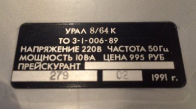
It was born in February 1991:
![]()
and was priced as about 4 monthly salaries of an engineer in that time...
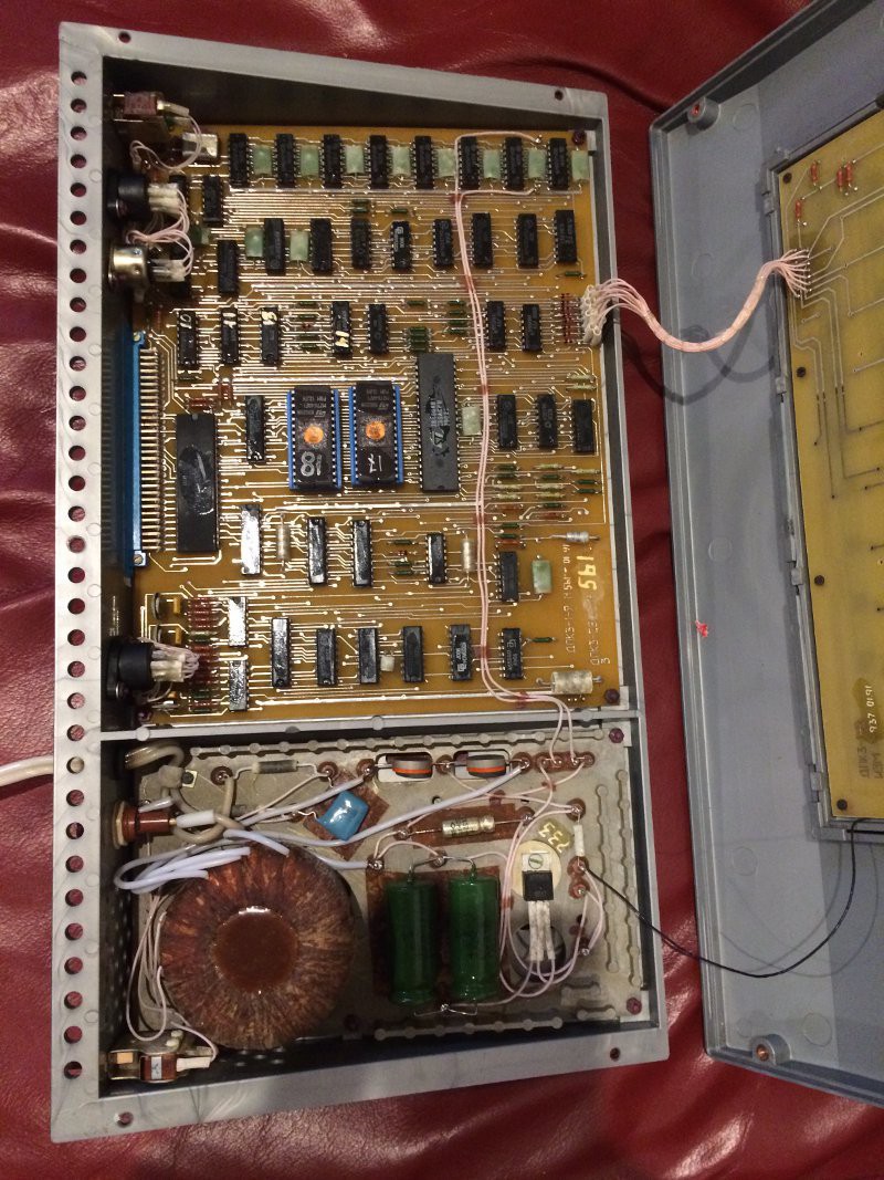
Hardware was completely original, built out of Russian parts (except for Z80A processor and ROMs), but ZX-Spectrum compatible:
![]()
Instead of edge connector, as regular Sinclair machine usually had, this one has a cloned 8255 chip with 24 general IO lines on the back (and third of it was used to implement Kempston joystick) and I used this IOs to extend the machine with quasi-disks and other peripherals - now it's time to finish that activity :)
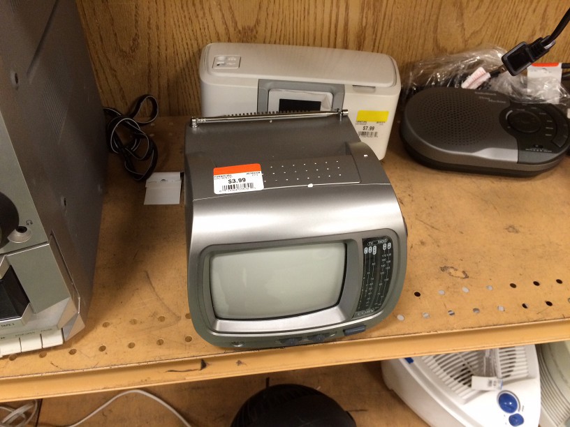
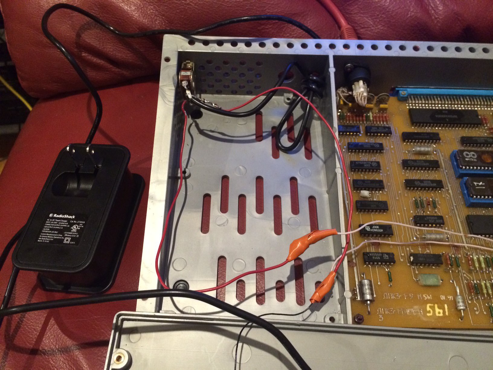
I threw away a power circuit because it's 220V and I'm in US now, instead I bought new 5V power adapter in RadioShack and connected it to the machine directly:![]() Another problem was to find TV that could recognize PAL/SECAM timings and usually it's a lottery because TVs in US may officially do NTSC only and you need to try to make sure that it may or may not be adjusted to recognize different video system:
Another problem was to find TV that could recognize PAL/SECAM timings and usually it's a lottery because TVs in US may officially do NTSC only and you need to try to make sure that it may or may not be adjusted to recognize different video system:![]()
This one was good (thanks to V-HOLD potentiometer on the back of the TV) and machine actually works now as if it was NOT 25 years since it was manufactured :)
![]()
I think it's important to say that this machine was completely illegal because it used modified copy of ZX-Spectrum-48K ROM image with a change of boot prompt from Sinclair copyright to (R) УРАЛ 8/64К and also it had second Russian font to print this new message...
-
Current Progress
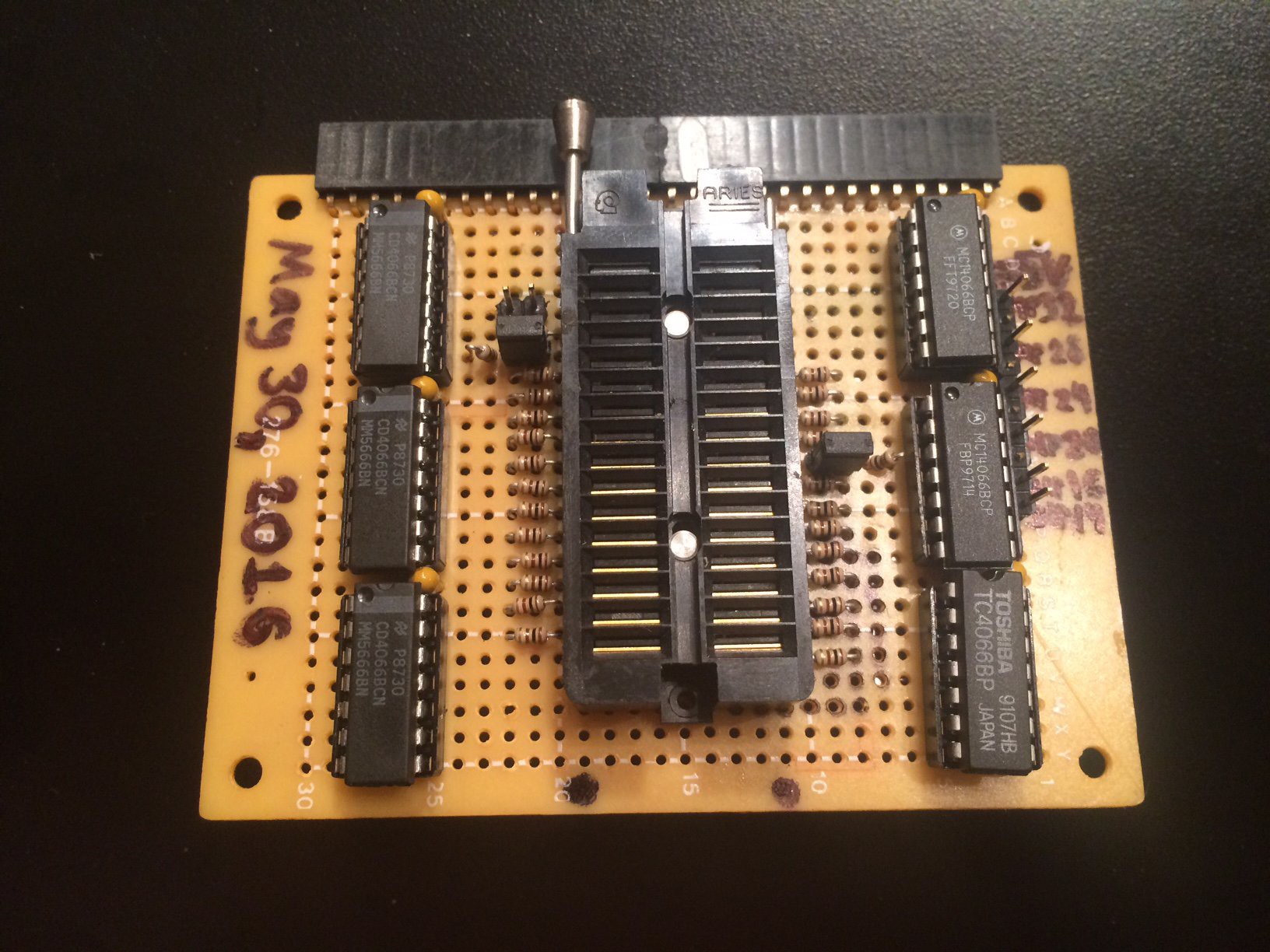
05/31/2016 at 03:10 • 0 commentsI didn't go too far unfortunately :(
![]()
It will be another smaller board connected to it and then they will be connected to some sort of interface that I designed in 90s for some micro computer that didn't exist in real life :)
-
Main idea
05/30/2016 at 19:24 • 0 commentsMain idea of the design is to read value from every pin through buffer and put zero on input pins by selectively connecting it to the ground while it's pulled up by default (with optional short circuit to +5V to provide optional power on some pins):
![]()
READ is a signal that connects one out of 4 octal buffers to data bus (OUTPUT). ZERO BIT is a signal from one bit of one out of 4 octal registers storing data for every single input pin of tested device. Resistor 100 Ohm is a kind of protection against accidental connecting output pins of device to ground. Pull-up resistor 10 KOhm is making sure that all pins will have at least "1" on them (also it will work for open-drain outputs of the tested device).
Old school IC tester
Old school integrated circuit tester/programmer, 100% open source, fully DIY and connectable to anything that provides 11 digital GPIOs
 Another problem was to find TV that could recognize PAL/SECAM timings and usually it's a lottery because TVs in US may officially do NTSC only and you need to try to make sure that it may or may not be adjusted to recognize different video system: