-
Status update
11/20/2021 at 18:35 • 0 commentsThe project was originally prompted by my disappointment over the Gamebuino META not being open hardware, like it's predecessor Gamebuino Classic had been. I set out to develop a board that would incorporate the respective consoles' MCUs (an ATSAMD21 and ATmega328, respectively), using an FPGA to emulate all peripherals such as the LCD, and provide a TV output for big-screen gaming. The "Chinese clone" branding was part of the flavor.
It was an ambitious project and now it is clear that it will never be finished in its original conception, but I would still like to present some of the technical design.
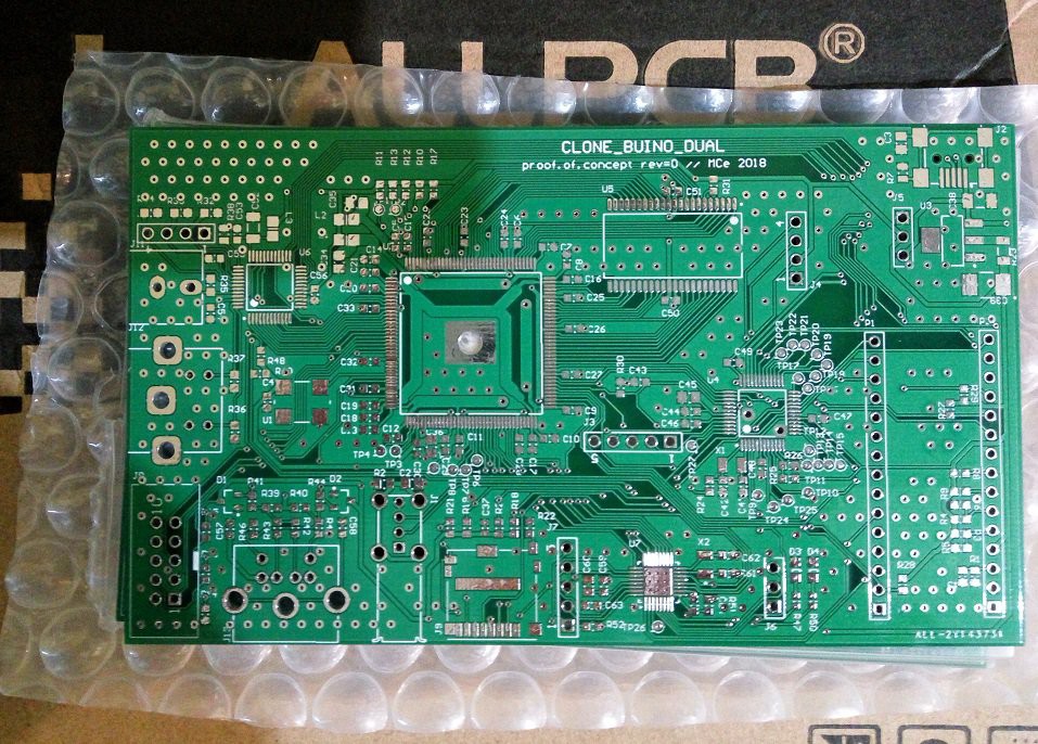
At the heart of the 2-layer board is the MAX10 FPGA (10M08SCE144C8G). However, the FPGA, being big and dumb, is at the mercy of a "system management controller" (SMC) represented by an ATSAMD21E15B-MU MCU. But it's not the only Atmel on the board; to emulate the Gambuino META, there is an ATSAMD21G18A-AU. For lack of better terminology, I will refer to it as the "application processor". There is no CPU on-board to emulate the Gamebuino classic, but there is a header that accepts an Arduino mini. Further we can find an CS4954 PAL/NTSC encoder, a 64kx16bit SRAM, and a bunch of I/O ports (PS/2, microSD) and programming headers.
The SMC has a number of responsibilties:
- execute a "BIOS" to orchestrate everything
- configure the video chip via I2C
- set registers in the FPGA to change operating modes (META/Classic) and stuff like display resolution
- handle inputs from an USB keyboard and translate them to GPIO for the application processors
- mix sound output and convert it with its integrated DAC
There were some compelling reasons to use a dedicated MCU rather than a soft CPU in the FPGA:
- built-in USB controller
- built-in DAC/ADC
- mature-ish software stack and debugging experience
I got as far as running code on the SMC and displaying text on-screen, entered with an USB keyboard and rendered by the FPGA. However, it never got as far as the gaming part.
Recently I have been contemplating whether the board could be reused for a more interesting project: a lo-fi custom GPU. It would require swapping the RAM for a bigger one (128k is just enough for a single 320x200x16-bit framebuffer) and slapping on an FTDI USB<->FIFO interface in place of the application CPUs. The SMC would be probably preserved to handle the I2C.
-
Initializing the CS4954 video generator chip
10/25/2021 at 21:27 • 0 commentsI have written about this on my blog here:
-
BEWARE of Quartus JTAG Programmer on Linux
04/29/2018 at 08:09 • 4 commentsIf you plug in your eBay "Altera USB Blaster" and try to talk to you device, chances are you get an error such as this:
/opt/intelFPGA_lite/17.1/quartus/bin> ./jtagconfig -d
1) USB-Blaster [2-2]
  Unable to read device chain - JTAG chain broken

  Captured DR after reset = ()
  Captured IR after reset = ()
  Captured Bypass after reset = ()
  Captured Bypass chain = ()
  JTAG clock speed 6 MHz
This would usually indicate that something is wrong with your board, the power, the FPGA, or perhaps the programming cable. Don't despair!
There is a known issue which is still present in the latest versions of Quartus. It has to do with a library called libudev. It is easy to find solutions for various distros, but I haven't seen one specifically for Fedora (27). In my case, what worked was:
ln -s /lib64/libudev.so.1 /lib64/libudev.so.0
Now the board is detected and can be programmed.
What have I learned? If you can't 1-800-JTAG to your board, check with a known-good board to quickly find issues on the PC side.
-
修訂版0印刷電路板的到來 [The arrival of revision 0 printed circuit board]
04/25/2018 at 18:30 • 0 commentsTBH, it will be a great success if anything works on this 2-layer mess!
![]()
 Martin Cejp