Jithin
-
Schematic
07/11/2016 at 07:14 • 0 commentsA breakdown of the schematics : Full schematic is part of the design package in github.
![]()
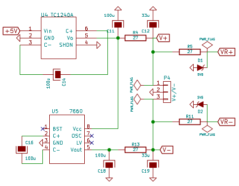
Figure : Bipolar power supply generation using charge pumps
![]()
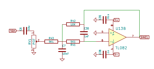
Multiple feedback filter for sine wave generation.
The values were simulated using a calculator hosted by OKAWA electric design![]()
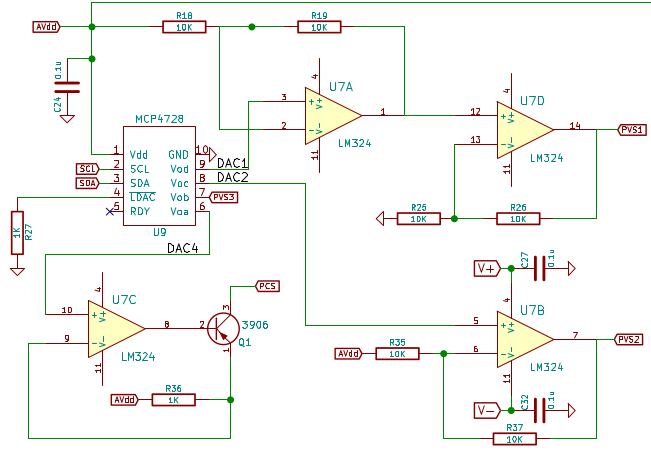
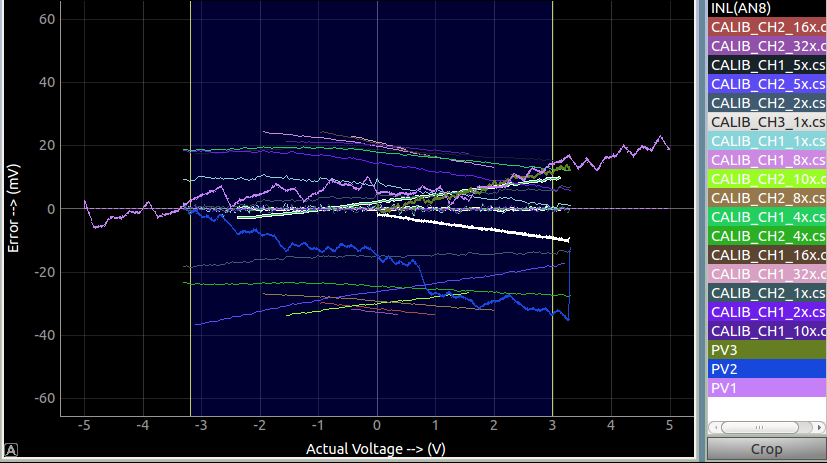
Using a 4-channel DAC to drive three voltage sources, and a current source. This model has high error margins, but since these are always consistent with the reference voltage, a point by point calibration(4KB per channel) can be used to achieve the maximum resolution of 12-bits.
![]()
Figure : Calibrating the analog channels against a calibrated 24-bit ADC.
The jagged lines belong to the DAC channels. As is evident from the graph, these cannot be fitted against polynomials of a few orders, so I went ahead and stored the errors on a per point basis (with two more constants for autoscaling the errors to a 1 byte full range). -
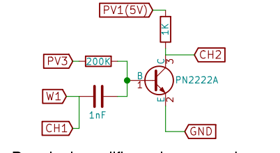
BJT Amplifier
07/10/2016 at 18:11 • 0 commentsAim: To operate the BJT as an amplifier in the common emitter configuration.
![]()
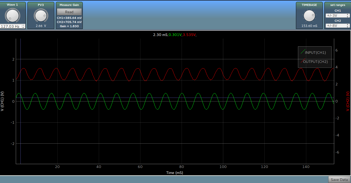
The input and output waveforms are traced on the oscilloscope using two channels. The gain can be calculated directly using the measure gain button. This experiment can be modified to calculate the bandwidth of the amplifier by varying the frequency of the input waveform and noting the corresponding gain.
Resulting Data:
![]()
The same can also be achieved using code
from SEEL import interface I=interface.connect() #fetch 5000 points each from CH1, CH2 with 2uS between each x,y1,y2 = I.capture2(5000,2) from SEEL.analyticsClass import analytics math = analytics() amp1,freq,phase,offset = math.sineFit(x,y1) #Calculate parameters of input waveform amp2,freq2,phase2,offset2 = math.sineFit(x,y2) #calculate parameters of output print (amp1,amp2,'gain = %.3e'%(amp2/amp1)) #calculate and print gain from pylab import * plot(x,y1) plot(x,y2) show() -
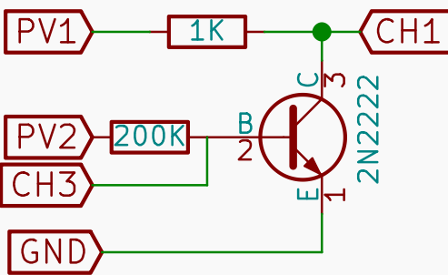
BJT output characteristics:
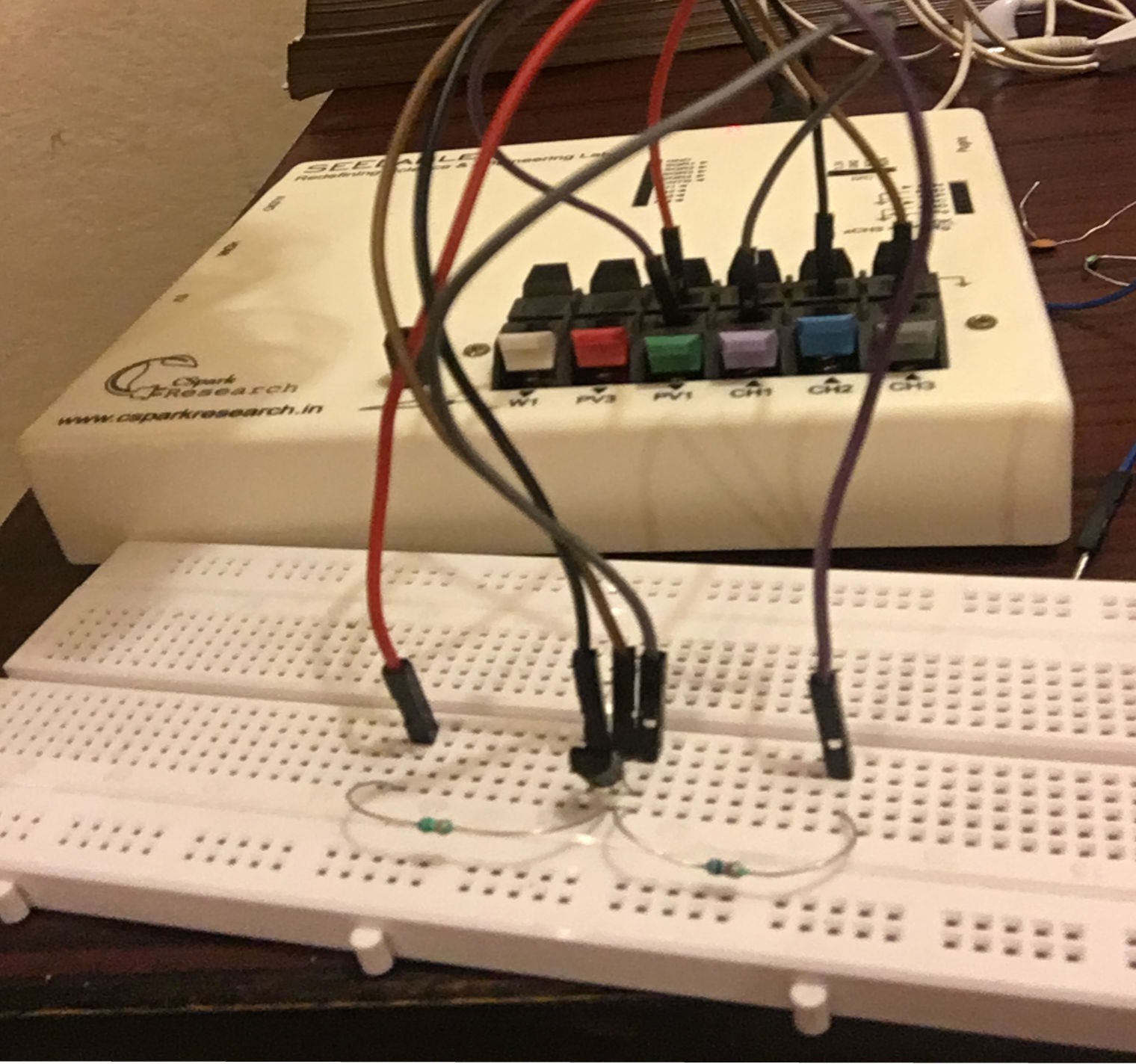
07/10/2016 at 17:38 • 0 commentsAim: To observe the output characteristics of a BJT on a curve tracer.
![]()
![]()
The base voltage (thereby base current) is varied and the corresponding I-V curve is plotted.
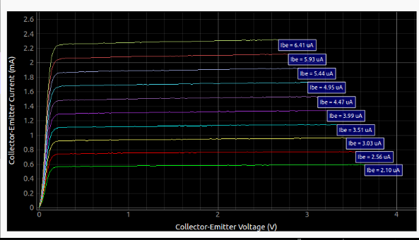
Resultant Data:
![]()
from SEEL import interface I=interface.connect() pv2 = I.set_pv2( 1.0) # Bias the base via a 200K resistor. base_voltage = I.get_voltage('CH3') base_current = (pv2-base_voltage)/200e3 # Use Ohm's law to determine current CollectorCurrent = [] CollectorVoltage = [] for a in np.linspace(0,5,100): pv1 = I.set_pv1(a) CollectorCurrent .append( (pv1 - I.get_voltage('CH1') )/1e3 ) CollectorVoltage.append(pv1) from pylab import * plot(CollectorVoltage,CollectorCurrent ) #Plot and try a different base current show() -
Experiment Designer : Design, Acquire, Plot
07/10/2016 at 16:26 • 0 commentsTo enable users to quickly put together a study of phenomena, a few control and readback elements have been incorporated into a common interface.
For example, a curve tracer for transistor CE output characteristics requires
A ) Base current setting : A parameter that only needs to be set once per curve
B) Collector voltage setting : A parameter that needs to be swept from Voltage A to voltage B
C) Collector current monitoring : A parameter that needs to be read for each value of B
In addition, the user may require plotting and analytics.Here's a video of our impression of what such a utility should look like ( LabView(TM) is ideal for such an audience, but there seem to be no FOSS alternatives to it yet ).
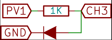
Diode IV is being plotted based on the following schematic. CH3 monitors the voltage drop across the diode, and (PV1-CH3)/1K is the current flowing through it.![]()
The derived channel section can also be used to add I2C sensors, and some thought needs to be put into adding an analytics section
-
A simple spectroscope using a linear optical array
07/10/2016 at 13:38 • 0 commentsLinear optical arrays (a camera with only one row of pixels), commonly used in barcode scanners, can be put to other uses as well.
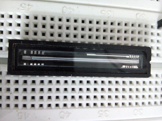
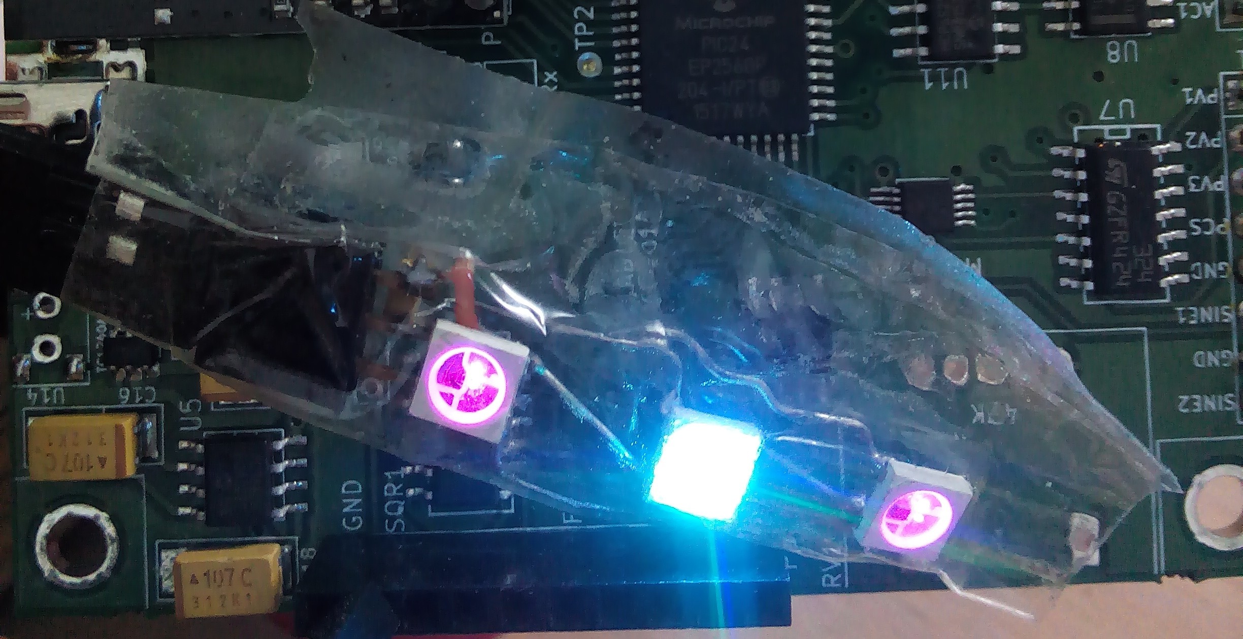
The SEELablet includes the ability to acquire data from one such array, and a simple diffraction grating was used to study the diffraction spectra of a few coloured light sources such as the WS2812B (RGB LED), a torch, and a laser diode.![]()
![]()
![]()
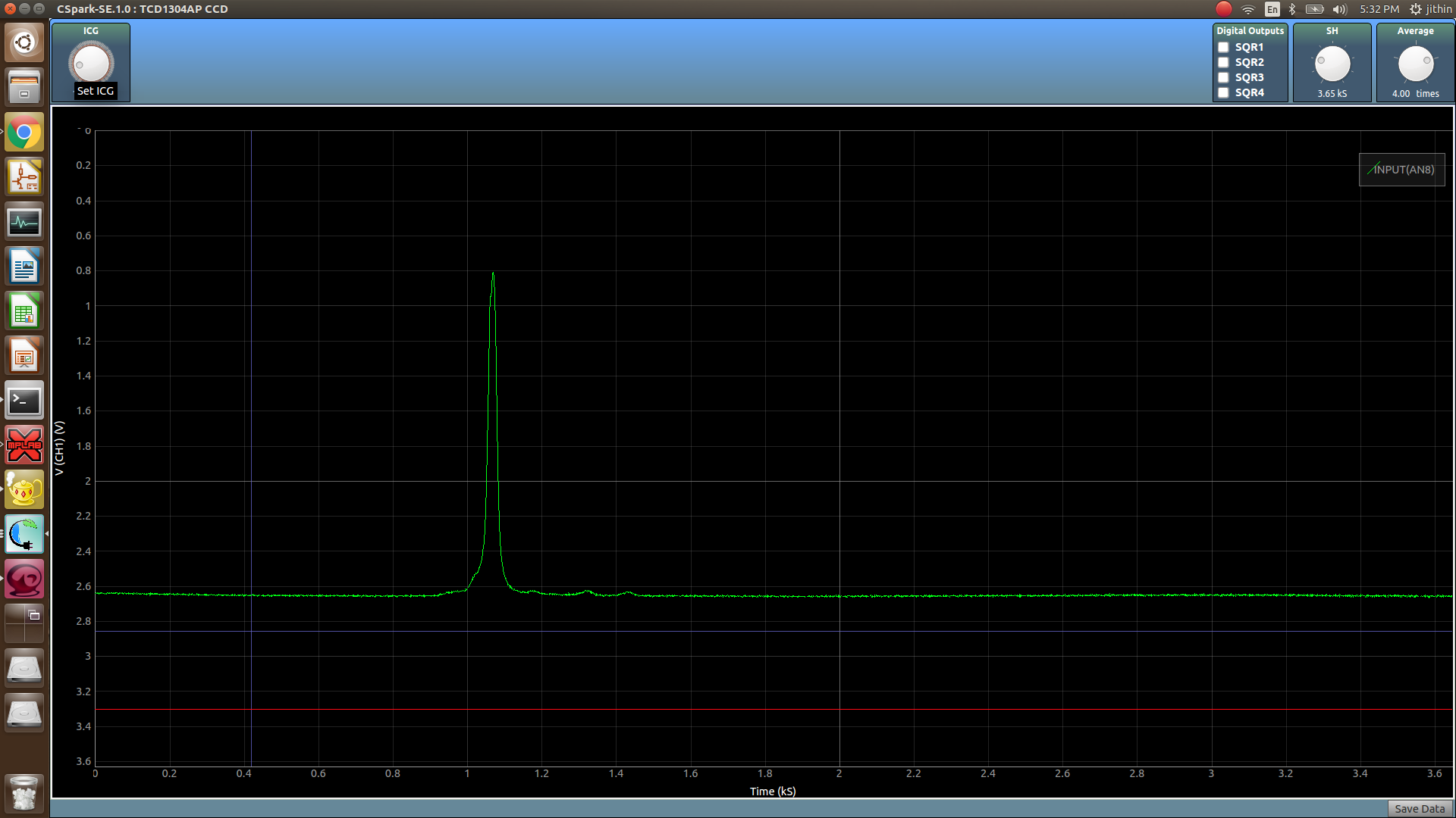
A ruler was placed on the sensor. Its opaque marking cause the spikes in the plot
Figure : Sensor element, and RGB LED
![]()
from SEEL import interface I=interface.connect() I.WS2812B('SQR1',[[25,0,0]]) #Set a faint shade of red on an RGB LED
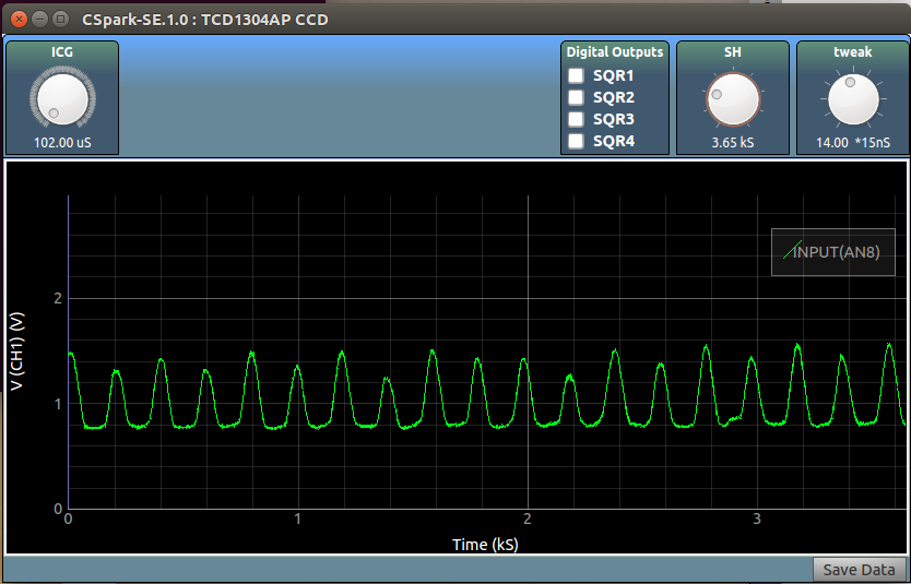
SH = 2 # time period of shift gate in uS ICG = 12e3 # 12mS integration time I.opticalArray(SH,ICG,'AN8',resolution=12) #acquire one set of readings I.__fetch_channel__(1) Y=I.achans[0].get_yaxis()[32:-14] #Crop out the dummy outputs from the sensor![]()
Figure : Shortest wavelengths to the left, infrared to the right. The peak for RED shows slight saturation here because I set ICG (integration time) too high. The color of the RGB LED is set using the color picker widget
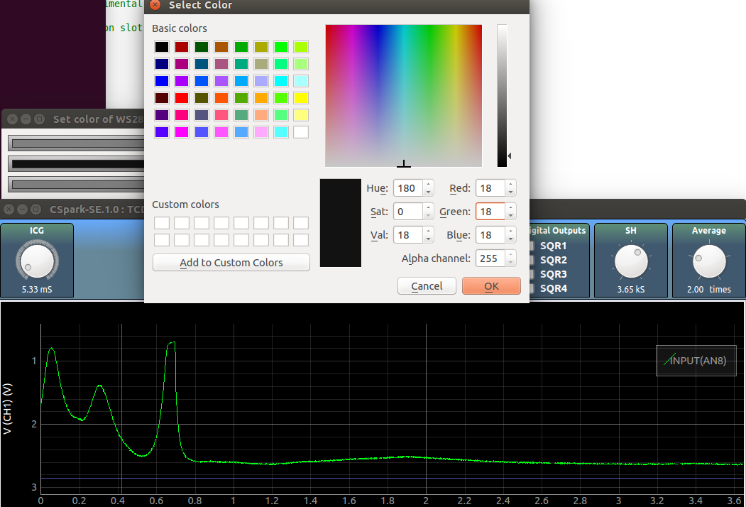
![]()
Figure : Green and blue peaks are visible if the colour is set to Cyan. The second order of the spectra is also visible
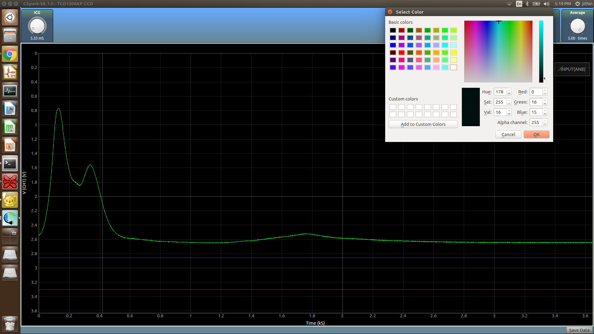
![]()
Figure : A laser has sharper spectra. Shown here is the spectra from a commonly available red diode laser.
-
Automated Assembly : Pick And Place
07/09/2016 at 17:51 • 0 comments
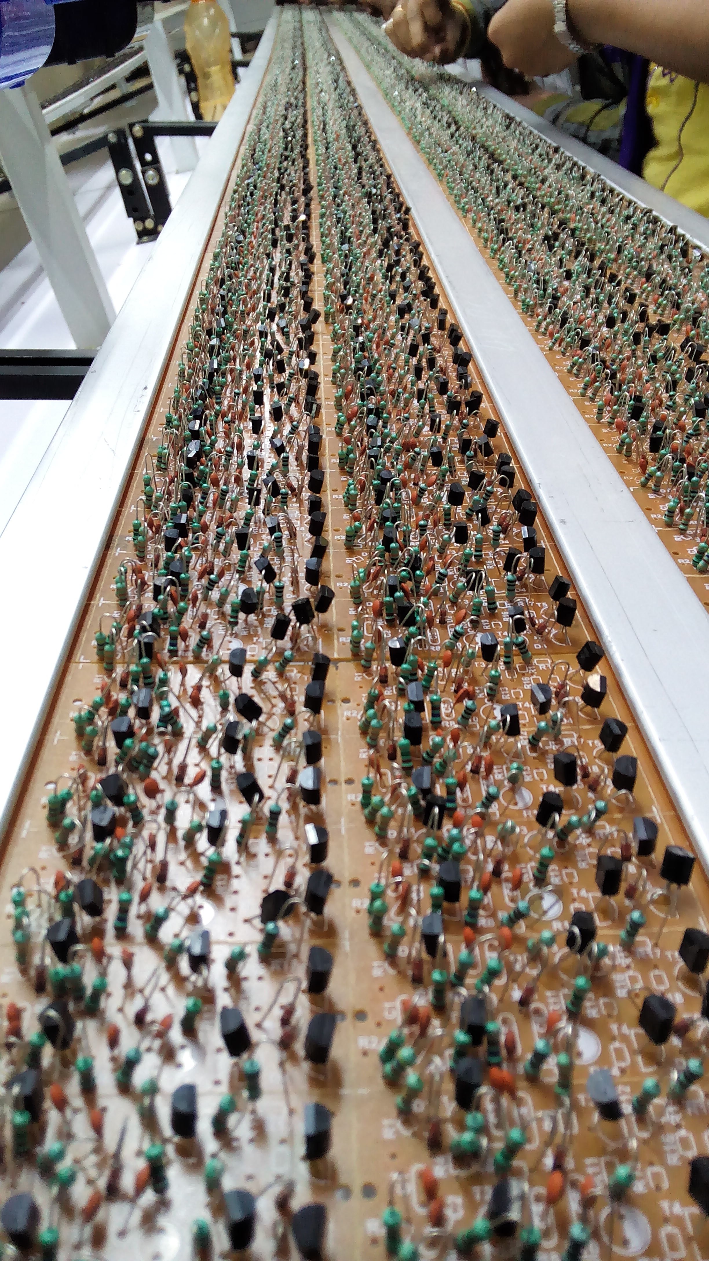
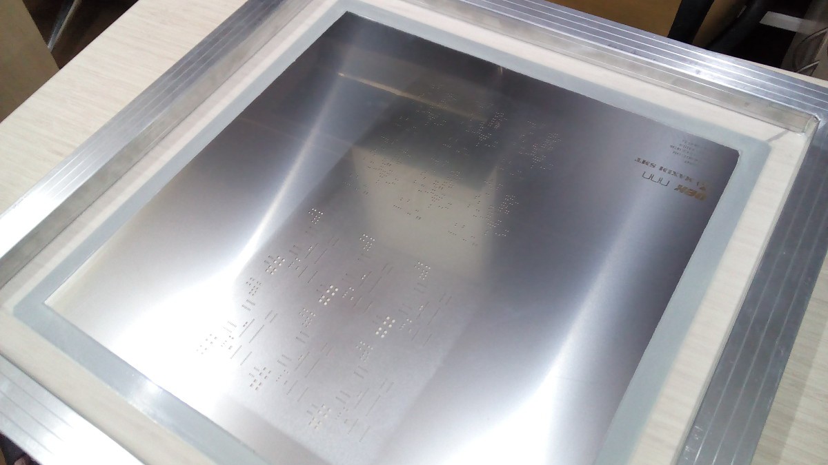
A Pick 'n place machine uses vacuum nozzles to pick components from their packages (Tape and reel, tubes, and even trays ) , and place them on their appropriate pads on the PCB based on a preloaded coordinate file. Prior to this, the pads on the PCB are coated with a layer of solder paste using a stencil.![]()
The machine also uses image processing to check if the components have been picked up properly, and also makes corrections if they've been picked up with slight rotation or an offset.![]()
![]()
Figure : applying the paste. and the stencil for the panel.
![]()
Figure : The pick and place machine. I didn't order the PCBs in panel form with margins , so a custom rig had to be designed in order to feed the PCB into the Machine. It's much easier with panels though.
![]()
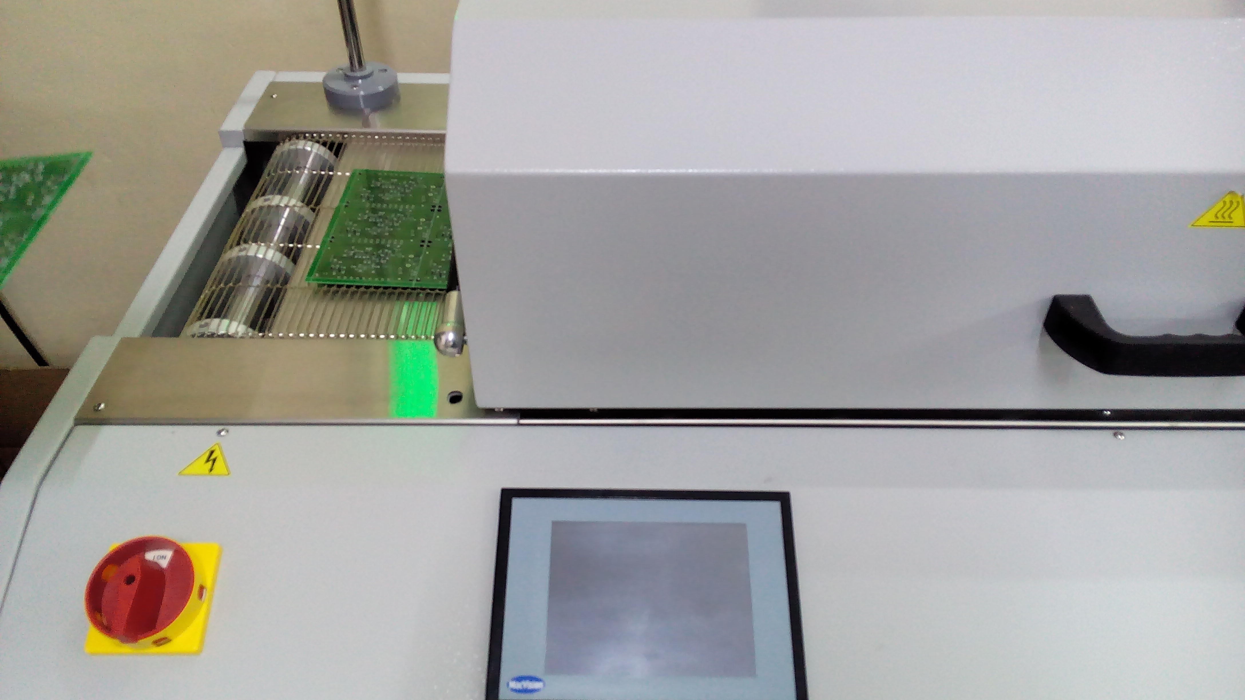
Figure : static reflow process. The oven's temperature follows a preset curve, and a batch of PCBs(whatever you can fit inside it, avoiding the extremities) reflow in about two minutes.
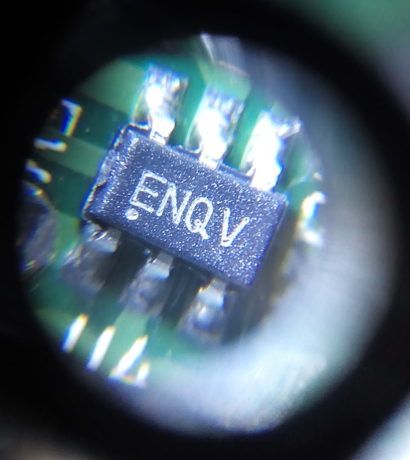
![]() Photograph of a reflowed component( voltage doubler ) taken with a phone camera attached to a microscope lens.
Photograph of a reflowed component( voltage doubler ) taken with a phone camera attached to a microscope lens.![]() Reflowed boards. The PicKit 3 has a Programmer-to-go option where a HEX file can be downloaded onto it once, and the computer+IDE is no longer required. It can be powered from any source, and the code can be downloaded by pressing a physical button. Came in handy for preliminary testing.
Reflowed boards. The PicKit 3 has a Programmer-to-go option where a HEX file can be downloaded onto it once, and the computer+IDE is no longer required. It can be powered from any source, and the code can be downloaded by pressing a physical button. Came in handy for preliminary testing.
![]()
Figure : A conveyor based reflow oven. The boards travel slowly through various temperature ranges maintained inside the tunnel, and the reflow happens as it moves.
A manual assembly line at the workshop!![]()
-
Painting , Printing the enclosure
07/08/2016 at 05:26 • 0 commentsSurface Texturing
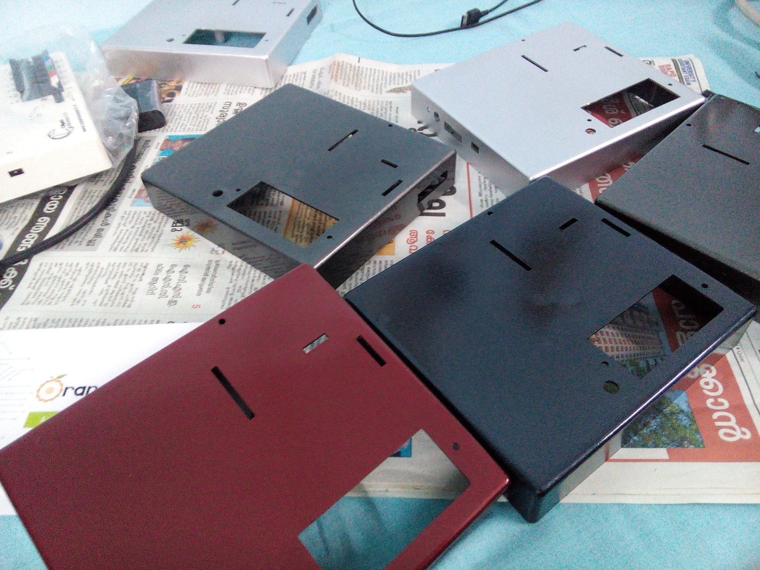
Injection moulded plastic may not have the required surface finish unless one invests heavily in a high quality die textured using a large copper plate using EDM. Diamod polising the die is affordable , but glossy plastics are prone to scratches and easily pick up fingerprints and grease . In most cases (Toys, Back panels of tablets... ) , a layer of paint is added to the surface. A few different options were explored for doing this, and the local auto workshop also obliged by spray painting a few sample boxes .
Here are the results
![]()
I painted the silver box in the corner using a regular spray can.
Printing
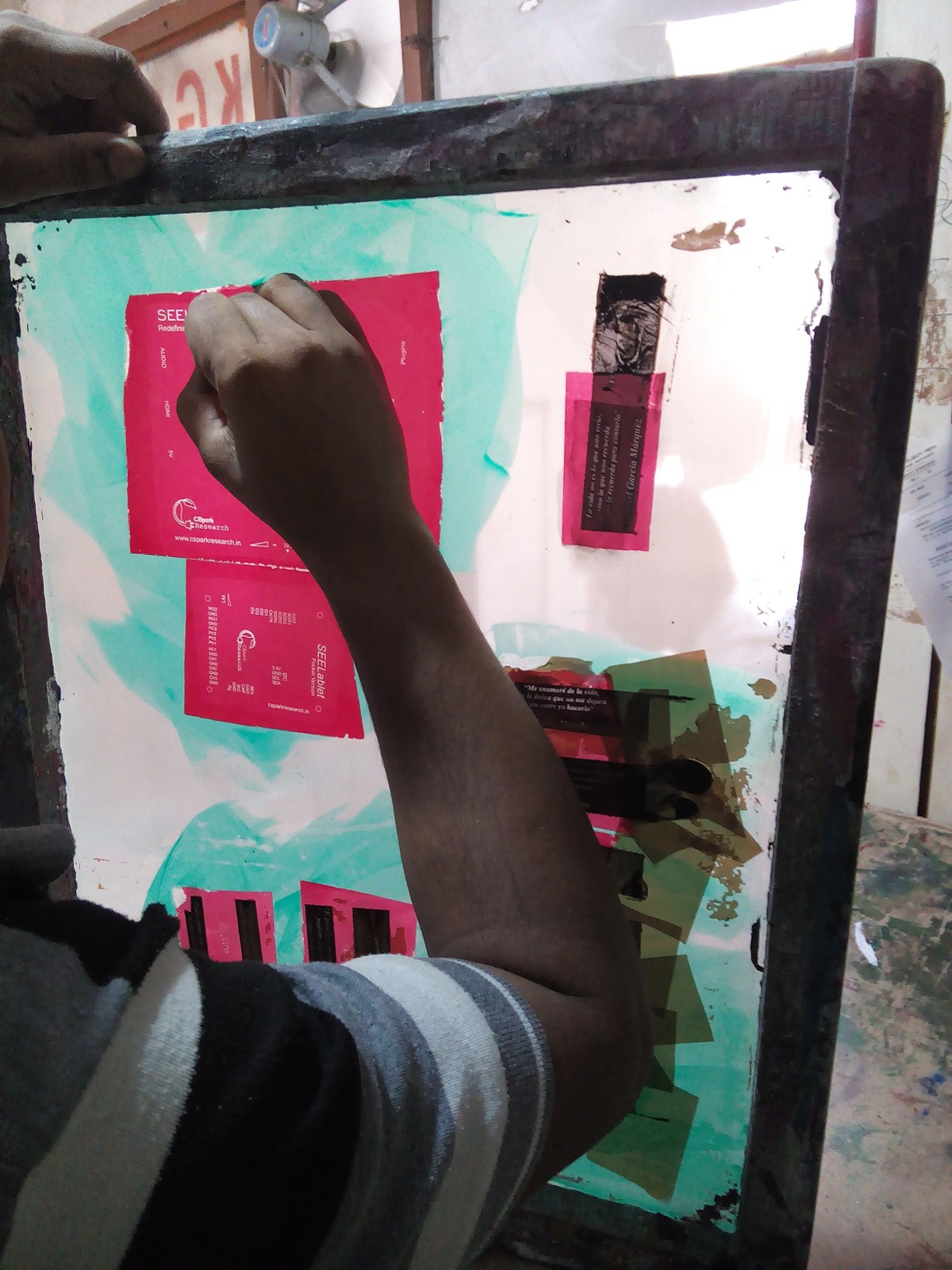
After a couple of manual screen printing attempts, I finally settled on pad printing.
Manual screen print involves etching a patterned photoresist pasted on a porous membrane. Photo:![]()
Here's how it looks along with the frame
![]()
The frame is placed on the surface to be printed , and a rubber pad is used to drag a thick layer of ink over the stencil.
Results with manual screen printing:
![]()
Finally settled on PAD printing, which is more expensive, but has much sharper resolution.SVG version of Printing files . Even though I feel InkScape is far better and friendlier than Corel Draw, local workshops for laser cutting , pad printing, and even graphics printing insist on CDR files.
-
Student proofing : Designing a durable enclosure
07/07/2016 at 19:02 • 0 commentsLast year, I was set on using Acrylic for housing the project. I had however, also tried out a 3D printed case , but 3D printing is not for mass production.
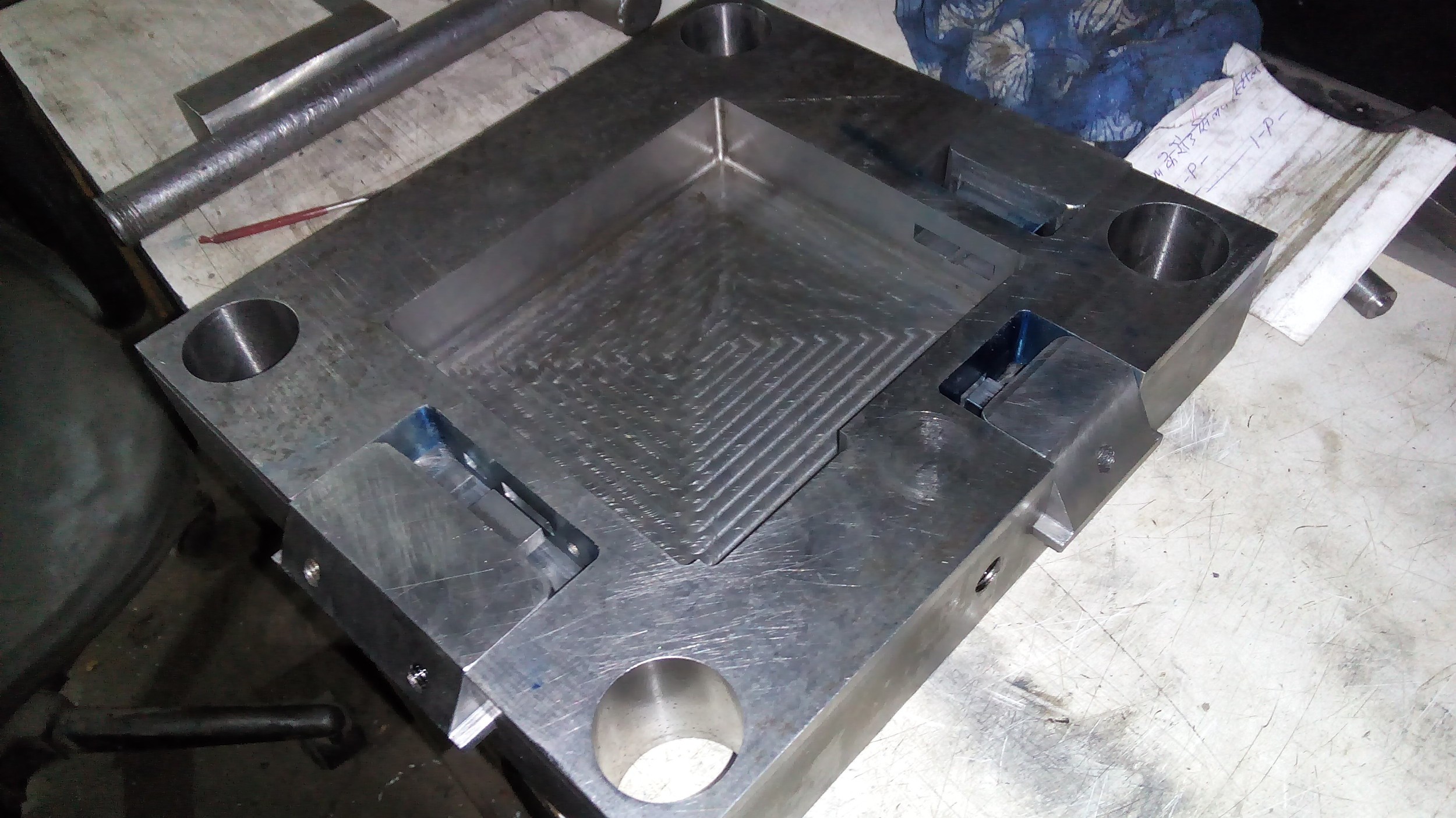
Injection Moulding , a process where fully formed enclosures are churned out by the minute, is more suitable for larger quantities. Although it involves an initial effort of CNCing a metallic mould for molten plastic to flow through, the results are worth it.
Here's a picture of the mould we made. The larger cavities have been dug out by a CNC , and the finer features will be machined using a conventional milling machine and sandblasting tools The sliding structures on the sides will lock into place while the plastic flows, and will create holes for USB ports, AUX sockets etc in the side walls. After this, they withdraw automatically so that the piece can be ejected without breaking![]()
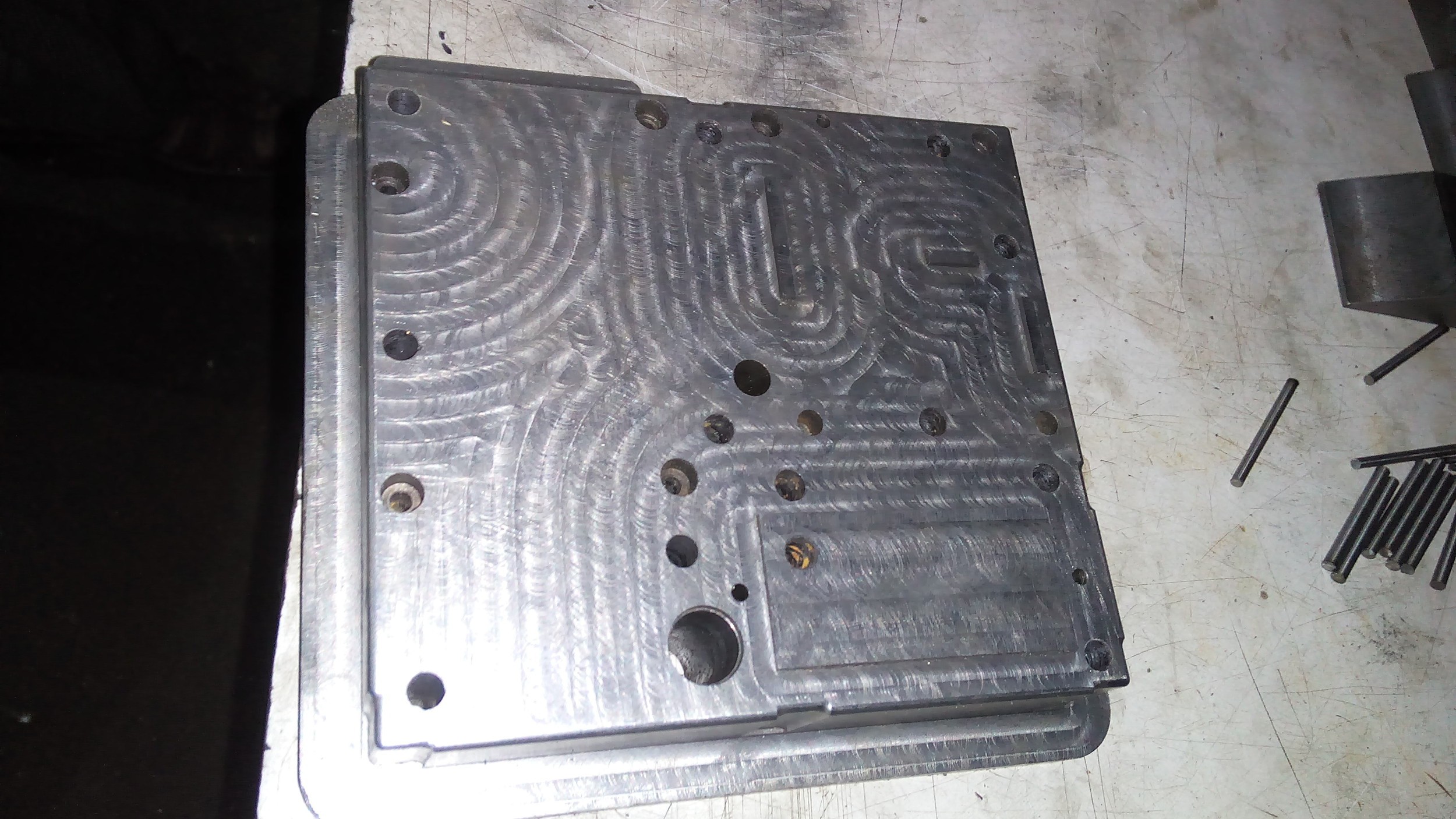
And here's a partial segment of the counter mould which will fit into this cavity, and leave a 1.5mm gap all around.
![]()
Most of the holes are for ejector pins. Once the plastic has flown through the gaps, and the mould has cooled and separated into the two separate halves by a large hydraulic assembly, they push against the plastic enclosure in order to separate it from the mould.
![]()
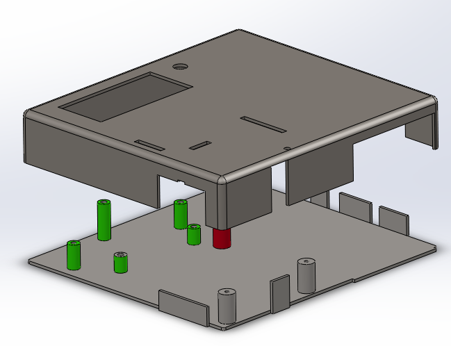
A CAD Render of the box. The side slots were later replaced with sliding inserts.
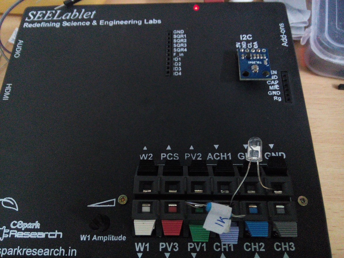
SEELablet : Instrument Cluster For Laboratories
Minimal, yet powerful combination of control and measurement tools integrated with an SBC running Python based UIs for science & Engg. Expts


 Photograph of a reflowed component( voltage doubler ) taken with a phone camera attached to a microscope lens.
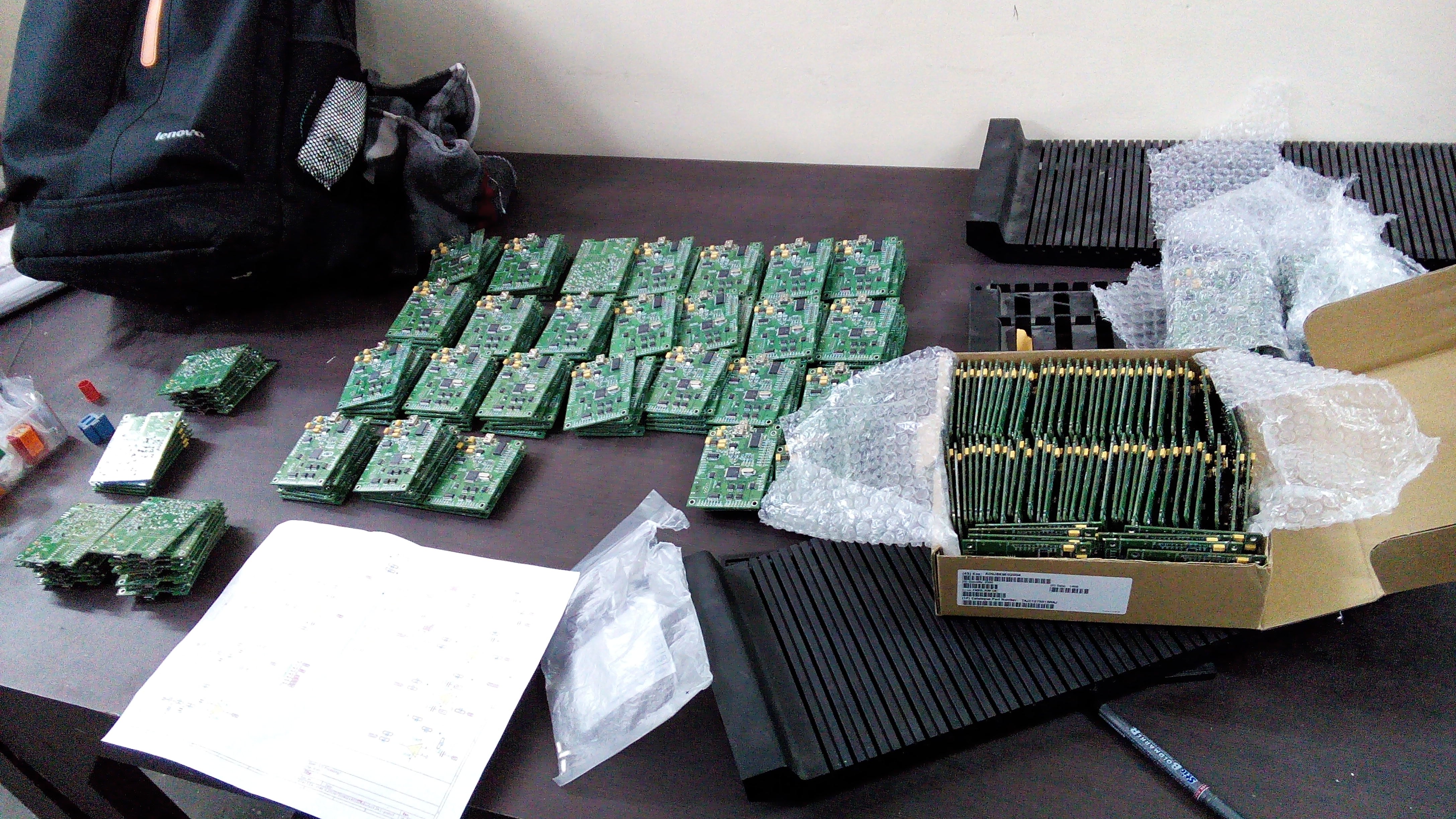 Reflowed boards. The PicKit 3 has a Programmer-to-go option where a HEX file can be downloaded onto it once, and the computer+IDE is no longer required. It can be powered from any source, and the code can be downloaded by pressing a physical button. Came in handy for preliminary testing.