Close
0%
0%

The 74LS181 ALU

Taming the 74LS181 ALU chip

Similar projects worth following
Taming the 74LS181 ALU

The 74LS181 is an old chip.
I first found it in my 1977 Motorola LS-TTL handbook.

At first sight it seems magical.
Upon review of the datasheet it is a mess!
The chip has some good functions and just as many useless ones.

Here is how I tamed it!

AlanX

Taming the 74LS181 ALU

First the useful instructions:
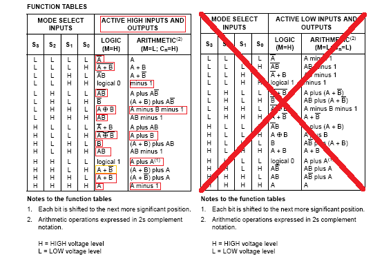
Okay you may disagree with my list but here are the reasons:

  • I am only interested in active high logic.
  • Of the arithmetic functions only every third one is useful.
  • I can do without MINUS.
  • The logic functions are a bit more subjective.
  • I have hi-lighted in orange one that is useful for my ALU because of the way it works.

So I got 16 codes, sweet now get back to work!

The ALU design for the 4 Bit CPU

For a 4 Bit CPU there are only 16 possible Op-Codes and I need to reduce the ALU set down to eight. You may not have picked up what I want! I really mean M, S3, S2, S1, S1 need to be remapped to 3 bits. Okay, but how do you do that, the codes are a mess!

First the eight codes I have selected:

  • PLUS (A plus B)
  • XNOR
  • LAST (B)
  • AND
  • DEC (A-1)
  • OR/NOT (A+!B)
  • OR
  • MOVE (A)

Note that A is now called MOVE and B is called LAST and will be discussed later.

You will note that I have chosen instructions for S3 high so my task is reduced to reducing 4 bits to 3 bits.

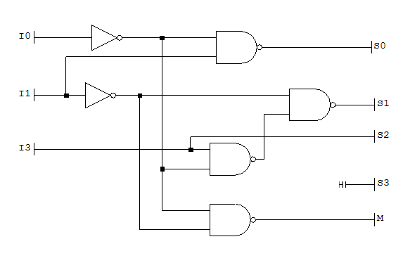
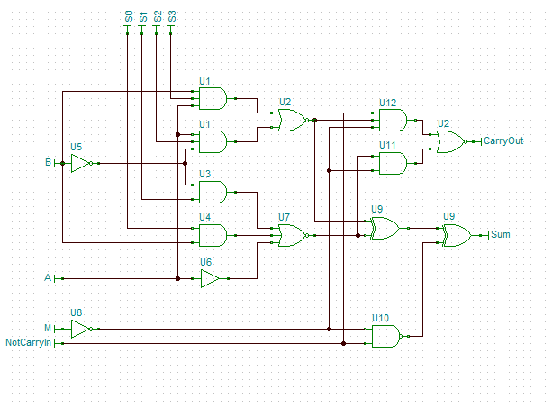
You will also note that other than ADD and DEC, the select codes (i.e. M, S0-S4) are unchanged. So I only need to remap ADD from 01001 to 11000 and DEC from 01111 to 11100. Note M and S3 are now always high. Here is the schematic for the remapping:
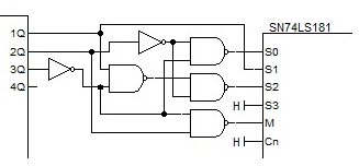
If your interested I did not solve the remapping by hand. I used LogicFriday:

LogicFriday is a front end for Espresso by Richard Rudell (rudell@ic.Berkeley.EDU).

ALU organisation for the 4 Bit CPU

I adopted a single register programming model for my ALU.

Basically:

  • Fetch data from the memory
  • Process the data
  • Deposit the result back to memory

For this to work then the previous results need to be reused as the "B" operand.

An ADD sequence would be:

  1. MOVE [Memory B] to [Memory B] (Sets the B operand)
  2. ADD [Memory A] to [Memory C] (A is ADDed to B and stored in C)

Okay what is with OR/NOT, LAST (B) and MOVE (A)?

  • OR/NOT (A OR NOT B) code was the closest available code remaining for use with the decoding decisions adopted, it us used to NOT the previous results.
  • The B code is the same as the LAST result.
  • The A code is the same as a MOVE.

Consider a NAND sequence:

  1. MOVE [Memory B] to [Memory B] (Sets the B operand)
  2. AND [Memory A] to [Memory C] (A is ANDed to B and stored in C)
  3. OR/NOT [Value 0] to [Memory D] (Not B and OR with 0)

Here the result of A AND B is NOTed and then ORed with zero, result is a A NAND B.

Here is the ALU schematic for the 4 Bit CPU:
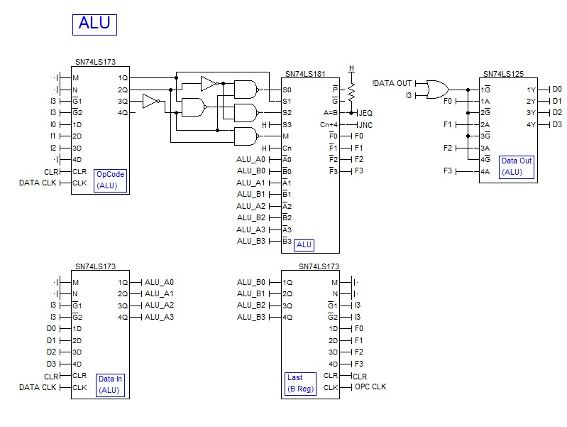
Are you still with me? AlanX

  • Schematic Error

    agp.cooper12/05/2016 at 23:36 0 comments

    Schematic Error

    Seems as though I mixed up the truth table when I designed the 181 ALU decoder. The schematic should be:

    regards AlanX

  • ALU III Revision

    agp.cooper08/14/2016 at 09:02 4 comments

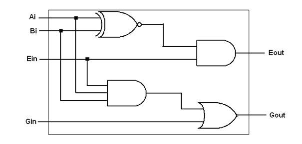
    I was trying to test the ALU design presented previously when I realized something was wrong with the comparator. Now where did that design come from? I could not find it on the Internet (surprising) but this one looked good to me:

    (source: http://fpgacenter.com/digit_dsgn/log_gates/comparator.php)

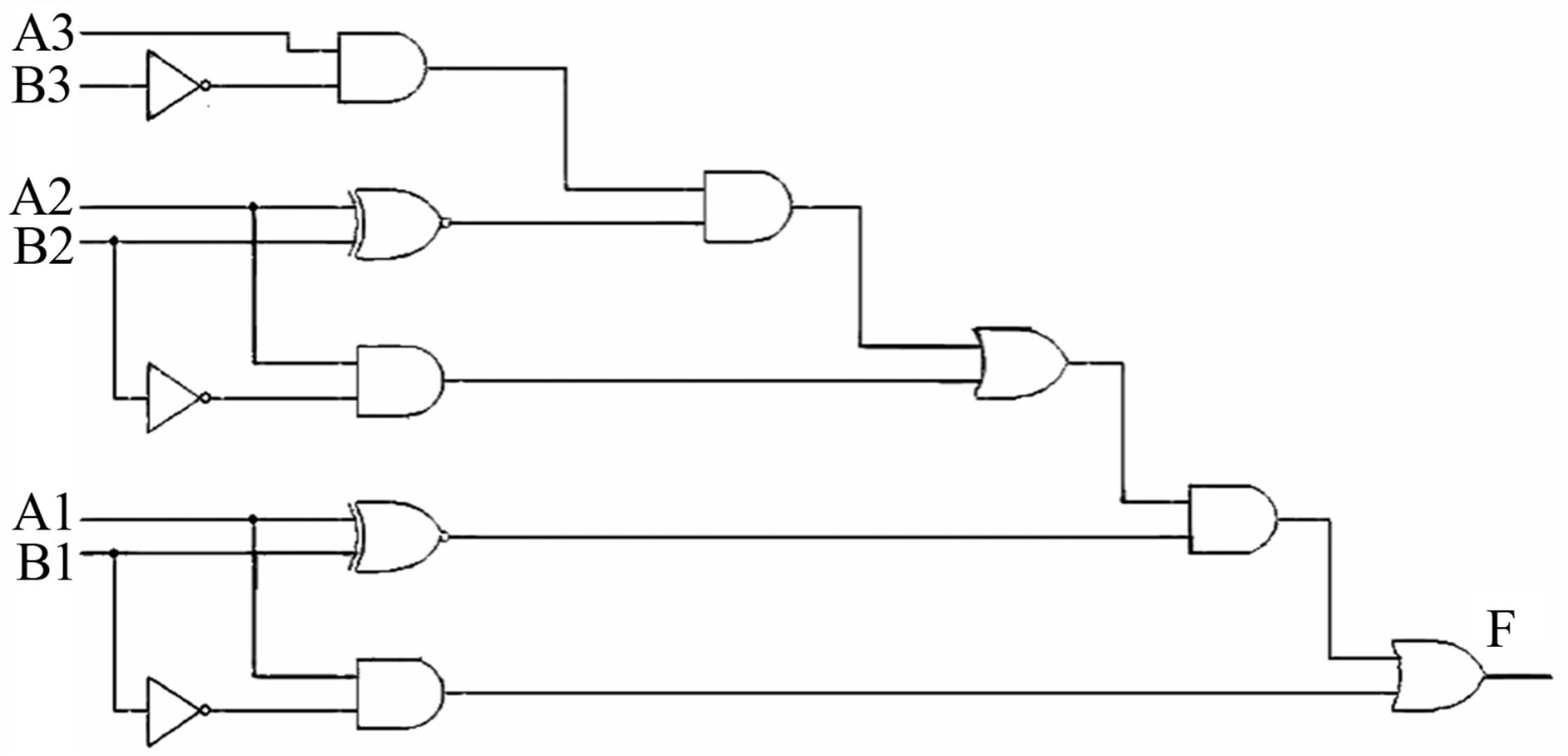
    Anyway, not happy where did it come from? Eventually I found this:

    (source: http://file.scirp.org/Html/2-7600304_41935.htm)

    Which I recognised I had used as a base. This came from:

    "Design of Low Power Comparator Using DG Gate" by Bahram Dehghan, Abdolreza Roozbeh and Jafar Zare.

    This is a A>B comparator only.

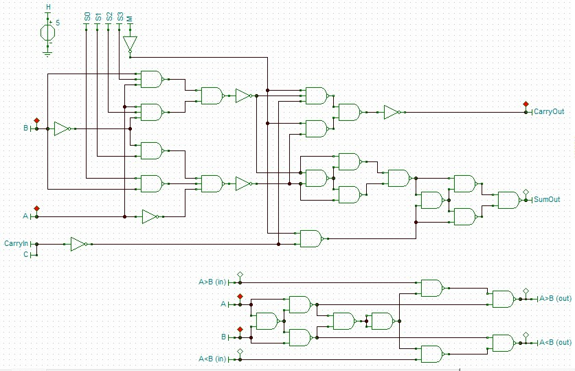
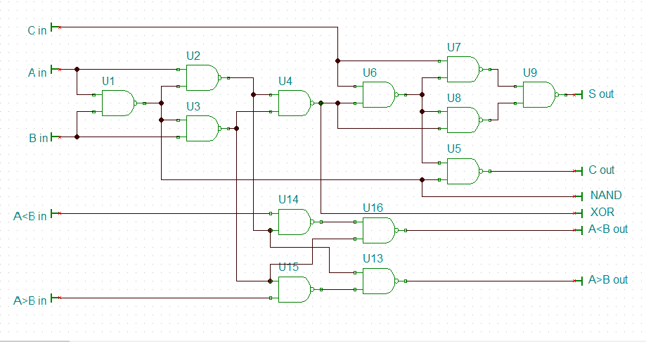
    So stripped out the bits I needed, converted to NAND gates and realized I could "mirror the circuit for A<B and reproduced my original circuit less the design error I had carried over. This time I did not to piggy-back off the ALU gates (so the comparator is now stand alone):


    The Hazards of Teaching Yourself

    In the above circuit I have some logic signal flags. Now I have had Tina Pro V5.5 for 10 years and did not know I could do this (the documentation is pretty bad). I have almost exclusively used Transient Analysis even for digital design. Now I am sure that if I did do a course then this feature would have been explained. (Note: I don't work in the electronics field. I was a mining engineer and we like to dig holes in the ground.)

    Because Tina Pro 5.5 is pretty unstable I migrated to the Tina-TI version (and that does not have logic signal flags). I was only using Tina Pro 5.5 because I needed something better than Transient Analysis. If I went back then I would have to re-digitize most of my current work as Tina-TI does not export the really old file formats.

    Crippled Software

    I have looked at Tina 10 but the hobby versions are crippled for only small circuits and the unlimited version are crippling in price.

    I have an old version of Cut2D (for CNC) that works really well and is unlimited. Cost about US$180 from memory a few years ago. The latest versions have gone the same way, crippled in capacity or crippling in price. Go figure! It not that there are no substitutes.

    AlanX

  • DIY ALU III

    agp.cooper08/13/2016 at 14:00 0 comments

    DIY ALU III

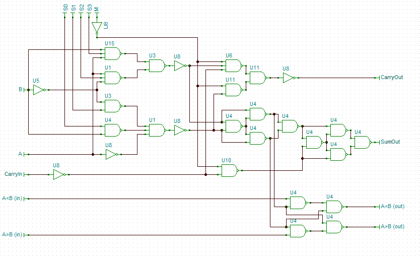
    Well I can't leave it alone! I decided to have a closer look at the 74181, so I extract a bit-slice from the schematic (the comparator logic is lost):

    Not hard, even found a schematic error - I wonder if anyone else has found it as well?

    I then converted the gates to NANDs, and added in my preferred comparator logic. Here is the result:

    So now I am down to 1 inverter for the Carry In (don't like the Not Carry logic of the 74181) and 27 gates per bit-slice. The main difference with my version is it will be slower to propagate.

    So the total gates for the 74181 was 100 and my version is 109 (but includes a better comparator logic). Add six gates for the Selection Decoder (refer to the 4 Bit CPU ALU issues) and I get 115 gates.

    This design would equate to seven packages per bit slice (much better!).

    I case you have forgotten why I an not using XOR gates or MSI logic, this work is in preparation for a possible transistor CPU, so it uses SSI NAND gates.

    I will have to look at the selection logic to see if I can fix it (another post?) or merge the Selection Decoder.

    AlanX

  • DIY ALU II

    agp.cooper08/13/2016 at 10:02 0 comments

    DIY ALU II

    I had a play with Logic Friday investigating a DIY ALU that matched the 8 functions selected for the 4 Bit CPU II.

    For reference the 74181 has 100 NAND gate equivalents (by my count).

    I coded a 1 bit ALU for:

    In(A), In(B), In(Carry), In(A>B), In(A<B), S0, S1, S2 -> Out(C), Out(Carry), Out(A>B), Out(A<B

    Where for S0-2:

    1. A ADD B
    2. A ADD !B (i.e. A MINUS B MINUS 1)
    3. OR
    4. AND
    5. XOR
    6. B
    7. !B
    8. A

    The result was:

    • 29 "prime implicants" (i.e. boolean equations)

    That translates to 37 NAND gates (with as many inputs as necessary).

    (The 37 equates to 8 inputs, 4 outputs and 29 prime implicants or PIs.)

    Therefore scaling up my ALU would result in 148 gates. Not unexpected as my ALU has no useless functions.

    Some experimentation (functions and function order) may reduce the PIs a little.

    Logic Friday also can produce a rationalise schematic based on standard packages, suggesting:

    • 2x Hex Inverter
    • 8x Quad 2-Input NAND
    • 4x Triple 3-Input NAND
    • 1x Dual 4-Input NAND

    So I will need 60 packages for my 4 bit DIY ALU! Perhaps I should just "close my eyes" and get to like the 74181!

    Or I could just copy the 74181 design and add my "pre-selector code" for 106 NAND gates (about 30 packages).

    No real headache using four 256x4 PROMs or a small PLA chip.

    AlanX

  • DIY ALU

    agp.cooper08/12/2016 at 03:56 0 comments

    A SSI ALU for my bit-slice CPU

    There is not much on the Internet about DIY ALUs if you don't like the 74LS181.

    For my Weird CPU I used an adder (74LS83A), a comparator (74LS85) and the NAND function (74LS00). I should have included the XOR and SHR functions as they were expensive to implement in software.

    Here is the schematic from my Bit-Slice SSI CPU (it is on hold at the moment):

    So you should recognise the NAND gate equilavent of an XOR gate (U1-4 and U6-9) that make up an adder (with U5). The remaining gates (U13-16) make up a comparator. I have also picked off the NAND and XOR outputs.

    Other than SHR it is all you really need for a DIY ALU. The rest is efficiently implemented in software.

    AlanX

View all 5 project logs

Enjoy this project?

Share

Discussions

monsonite wrote 10/19/2024 at 15:46 point

Hi Alan - I arrive a bit late to the party, but I have an ALU that might interest  you.

If we consider a single bit-slice, it consists of a full adder,  with an XOR gate on the B input , so we can selectively invert B when doing subtraction.

As we know, the full adder produces a sum term (XOR) and a Carry term (AND).  When we want a logic function, we can combine the AND and OR outputs in a 2-input multiplexer, (controlled by I4 and I5) which will give us ZERO, XOR, AND, and OR.

If you want  the inverted  logic functions follow the mux output with another XOR, to invert it.

When used for logic functions, you will have to suppress the carry from passing onto the next slice.


Diagram below,,

Regards

Ken


  Are you sure? yes | no

agp.cooper wrote 08/12/2020 at 07:15 point

Hi Ken,

Perhaps I am teaching you to "suck eggs" (after I checked your projects).

I have not explored the use of multiplexes in Logic Friday (or in the back end, Espresso) but it is there. I did check for this message, but I could not force it use during the schematic optimisation. So it may be worth while to have a look or maybe not.

AlanX

  Are you sure? yes | no

agp.cooper wrote 08/12/2020 at 06:41 point

The second question about "relays" is not too different.

Converting a truth table to a relay schematic I would not expect to be too difficult IF you don't try to take advantage of the many relay "tricks".

Simulation packages can model these relay "tricks" in any case.

I built a "trick" binary relay counter. The thing only works with a power supply that is 50% higher than the rated voltage of the relay. Basically, the design relied on the relay holding it state when the coils were in series (that is not "pulling-in"). And only pulls in when the coils were in parallel. It's tough to mathematically model these relay "tricks" in a general way.

AlanX 

  Are you sure? yes | no

agp.cooper wrote 08/12/2020 at 06:21 point

Hi Ken,

I think you are asking how do I check for logic error in my ALU schematics?

If so, then the way I do it is to write code (usually C) to create the Truth Table.

Yes you can do this by hand if the table is not too big.

I then import the true table into a logic design minimiser (such as Logic Friday).

Then I either:

Use the set of prime "implicants" (a reduced table) that can be used to create a "standard" (i.e. programmable logic array style) logic design/schematic.

Otherwise Logic Friday can create an optimised gate schematic for you.

Then to close the loop, the gate schematic is modelled in an Electronic Simulation program such as Tina to check the results.

An example of the method is:

  https://hackaday.io/project/13159-a-diy-keyboard/log/43905-remapping-the-keyboard

---

Something else you may not know if you are just beginning Logic Analysis, is that there are standard ways of converting a logic gate or gates from one type to another:

  http://electronics-course.com/image/nand-eq.png 

Regards AlanX

  Are you sure? yes | no

Ken KD5ZXG wrote 08/10/2020 at 15:57 point

16 functions of 74181 are exactly same as a 4way truth table, but in scrambled order.

Only 16 Fn(A,B) truths are possible. Any synthesis of all would create the same list.

/B is mutated into G by the rules of S1,S0: 00 Set, 01 Pass, 10 Invert, 11 Clear. Then AND with A.

/B is mutated into P by the rules of S2,S3: 00 Set, 01 Pass, 10 Invert, 11 Clear. Then OR with A.

Half result A plus Fn(A,B) is discovered by mixing XOR (P,G).

Fn(A,B) is not in order as we know 181 logic, but in the order we know 181 math.

Logic's "A plus" complication was hidden by re-arranging published functions.

Thus logic and math have the same 16 functions, but in different sequence.

/Carry or Mode (high for logic) may invert the final result /F.

For math, F = A plus Fn(A,B) plus C.

-----------------------------------

Up to half result is my possibly wrong understanding of how it works.

Beyond that point, math operations, I'm just paraphrasing Ken Sherrif.

Could be misunderstanding there too. We are not the same Ken.

I fixed an error regarding order of S1,S0,S2,S3. Should be OK now.

  Are you sure? yes | no

Ken KD5ZXG wrote 08/10/2020 at 15:22 point

https://hackaday.io/project/174243/gallery#2e77dd1d3bb09a2a06dbf1ae3b0aac14

Its the third drawing, if hackaday gallery misdirects you to the first...

Would appreciate if someone who knows 181 and relays might check for errors.

Timing assumes 74CBT multiplexer series. NC is the home position, selects low. 

  Are you sure? yes | no

roelh wrote 08/16/2018 at 07:03 point

Hi Alan, you might be interested in the 4-bit ALU that I designed, with only 7 TTL IC's, see https://hackaday.io/project/160506-4-bit-ttl-alu ! And if you want a transistor ALU, check https://hackaday.io/project/160177-alu-in-dctl-technology .

  Are you sure? yes | no

agp.cooper wrote 08/16/2018 at 13:40 point

Yeah, pretty good. I have not actually checked the schematic, but "B-A" should be "B-A-1" as just inverting the input is not enough. You need to set "Cin" high as well.

Still credit for a clever design.
The 74181 is really a pretty awful chip. Having built a few DIY CPUs all you really need is ADD and NAND and Jump On Carry. The other improvements (SUB, AND, OR, XOR etc.) just reduce the number of micro-instructions required. Still each to their own with regard to CPU philosophy.
The only other comment on your design (ALU_SQ4_schematic.png) is that you need a 5 bit wide opcode, nice if this could be reduced to a 4 bit wide opcode.
Regards AlanX

  Are you sure? yes | no

roelh wrote 08/16/2018 at 19:37 point

Hi Alan,  You are right about Cin, I added a comment about this in the description. In a new log I also described a simple conversion circuit to reduce the number of opcode bits to 4.

  Are you sure? yes | no

Yann Guidon / YGDES wrote 07/31/2017 at 04:53 point

For a decoder, I'll use the 74S188, for which I am making the #PROMer  :-D

  Are you sure? yes | no

agp.cooper wrote 07/31/2017 at 13:08 point

I had a couple of these chips for many year but in the end threw them out.

They are open collector and only 32 bytes.

If your designing your own burner you should have a look at the one I built for the Weird CPU. You may like some of the circuit design ideas or maybe not.

Regards AlanX

  Are you sure? yes | no

agp.cooper wrote 07/31/2017 at 13:29 point

Here is the schematic:

https://cdn.hackaday.io/files/12879551015136/PROM_PROGRAMMER.png

Quite a bit of work went into making sure the ramp up was not too fast or too slow (within specifications). The final schematic also has logic to read the written data.

Regards AlanX

  Are you sure? yes | no

Yann Guidon / YGDES wrote 08/01/2017 at 00:39 point

Hey Alan :-)
That's pretty nice, and a great addition to my References page !

Would you add a page to your project so I can link to it, or do I directly include your image in my page ?

Also : since the data lines go to high voltage, the programmer works for a certain subset of parts (such as National Semiconductors). Other parts require the data line to be grounded.

  Are you sure? yes | no

agp.cooper wrote 08/01/2017 at 03:52 point

Hi Yann,

I put it in the download files of Weird CPU.

The thing about the programmer was the voltage shift, the current supply and the ramp up. The solution is easy to adapt. I added a diode/resistor in the strip-board design so I could sense the output as well.

You can make a copy for you project page if you like.

Anyway, best of luck.

  Are you sure? yes | no

agp.cooper wrote 04/09/2017 at 01:13 point

Hi Dylan,
I would add that the compare function on the '181 is practically useless.
I ended up using a '85.
Best of luck AlanX

  Are you sure? yes | no

agp.cooper wrote 04/09/2017 at 01:08 point

Hi Dylan,
Great. I have used a version with my 4 bit CPU but have not tested it yet.
If you send you version of the design I will look it over, if you like.
Regards AlanX

  Are you sure? yes | no

Dylan Brophy wrote 04/08/2017 at 15:34 point

im going to use you decoder. It's a nice idea.

  Are you sure? yes | no

Similar Projects

Does this project spark your interest?

Become a member to follow this project and never miss any updates