-
Hello there, I am a Generative kAiboard
08/20/2023 at 22:49 • 0 commentsSeven years might seem like an eternity in the world of technology, where trends change in the blink of an eye. Yet, after enduring millions of keystrokes, weathered the presence of food crumbs and defied the rigors of unforgiving electrostatic discharge, I am elated to announce that I have returned. What's more, the keyboard that embarked on this journey with us all those years ago is not only still standing but thriving remarkably well even after continuous daily abuse.
Today, as a new chapter unfolds, I am delighted to unveil an evolution of innovation.
In an era defined by the extraordinary advancements in the field of generative AI, the fusion of technological innovation and the boundless realms of creative expression has blossomed to unparalleled dimensions. As we bear witness to the remarkable journey of generative AI, a transformational narrative unfolds before us, one where machines take on the role of creative collaborators. This remarkable evolution signifies the union of human ingenuity with the immense capabilities of AI, resulting in a paradigm shift that permeates various aspects of our lives.
Amidst this dynamic landscape, I am thrilled to introduce to you the Generative kAiboard – an embodiment of the intersection between artificial intelligence and human interaction. This keyboard stands as a testament to the convergence of two realms, where the ingenuity of AI is harnessed to amplify and augment human creativity. The Generative kAiboard signifies more than just a technological marvel; it is a gateway to exploring the synergies between the digital realm and our innate imaginative potential. With every keystroke, it invites us to engage in a harmonious dance of human and machine, allowing us to explore new horizons in communication, creativity, and connection.
![]()
Intrigued by this transformative journey? I invite you to witness the Generative kAiboard come to life in action through the captivating YouTube video below. Immerse yourself in the harmonious blend of technology and imagination that defines this remarkable creation. Your engagement is pivotal as we embark on this innovative venture.
Furthermore, if the Generative kAiboard has sparked your curiosity and resonated with your vision of the future, I encourage you to explore and support the entry in the Wiznet TOE Design Contest that is currently ongoing. Your presence and endorsement in this exciting competition would not only reaffirm our shared enthusiasm but also pave the way for a new era of creative exploration. Let's collaborate in embracing the potential of generative AI and pushing the boundaries of what's possible.
-
THP Judge: Anouk Wipprecht !
09/12/2016 at 22:30 • 0 commentsMaker Faire Eindhoven.
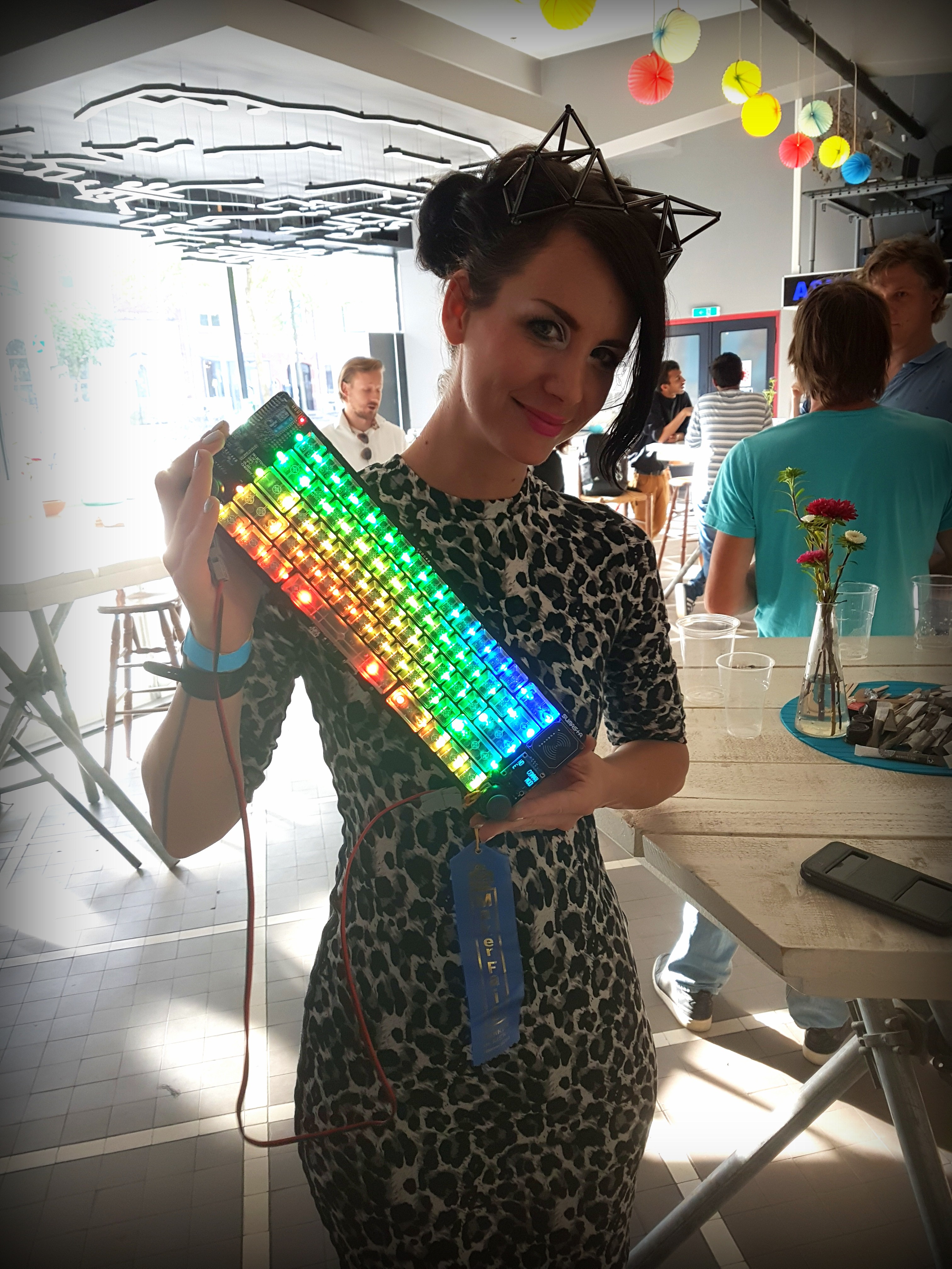
What a weekend it was. I've been to several Maker-Faire in three different continents, but yesterday was my first time attending Maker Faire in the Netherlands (Yeah, the country where I've been residing in the last 5 years). The atmosphere was amazing and the enthusiasm was all over the place. Didn't realize there are so many makers just around the corner. I strapped myself with the F/society Keyboard, RGB glasses and riding Electric unicycle all along the event, had to say even as a visitor I attracted quite some attention. :)
But but but.... the highlights of the event was meeting the one and only; Anouk Wipprecht. Yes, one of The Hackaday Prize Judge for this year event. She gave a talk as well as leading a Make-athon during the event. I actually joined the Make-athon on the second day and it was such a pleasure to be guided, helped and mentored by her. Thanks Anouk!!
![]()
Firmware
On top of that, a small follow-up update. The pre-release firmware of this project is available on Dropbox. There are still quite some clean-up will be done. Hardware pre-configuration also will follow.
-
Updates & Maker Faire Eindhoven
09/08/2016 at 19:51 • 0 comments![]()
Well, been around 5 days since the last update. It has been pretty busy week for me as typically; leave home 7.30 in the morning and arrive home at 23.45 midnight. Between work-stuff I've been trying to make some progress for this project. For this week I think I can summarize in bullet points below:
- Software Update:
- Some restructuring was done in the software. Which pretty much almost ends up like rewriting the whole thing. Though at this point I am a bit more satisfy with the progress. Does the job pretty well as my casual keyboard with additional personal flavors on top of it. Of course I am open to improvements from the community. In short I've been trying to really simplify the syntax and way the code works etc. So I hope people with little programming background can understand and adjust the software as they want it.
- Github's on the way. I just need to allocate some time to properly set it up. Hopefully this week.
- Hardware Update:
- As covered in my previous log. I am currently busy with making the second version of this keyboard. There are plenty of feedback from the community and I am trying to accommodate those feedback as much as I can. I hope having more features on the will attract more and more people to try recreating this project and eventually become the keyboard that they'll use daily for the rest of their life :) In general the proposed changes are:
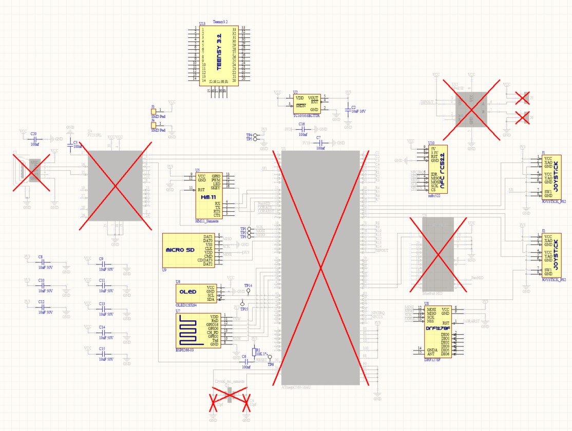
- Wired Variant. In my previous log I mentioned that i will implement teensy as the alternative component on the board for wired version. However, after some considerations, I am now changing the plan. Having 2 variants in which both uses different type of uC, it might in fact introduce some 'confusions' in the firmware part. Because of the difference, one will be more developed than the other etc etc. So the rplan is now for the wired version, I am now replacing the ATMEGA328p as the co controller on the board to ATMEGA32u4. As you might haver known, ATMEGA32u4 has built in USB peripherals embedded for HID stuffs. So I am sure this won't hurt much. So in conclusion, for both variants, ATMEGA2560 will remain as its primary controller.
- Bluetooth HID. As it is now, I am currently using bluefruit HID with embedded HID firmware ready out of the box. However, I do understand that this part is actually getting more and more scarce; or in other words harder and harder to get. Also the price for some people might be a bit much. As I menationed earlier, the options are either going to WIRED version of use alternative bluetooth Module. So in the next version of the PCB design I will provide 2 footprints either Bluefruit EZ key or alternative. At this point in time, my eyes are on to the famous Bluetooth HC-05. There has been many firmware hack flying over community about this bluetooth module, so I think it is a wise option.
- Additional RF Module. In the current design, I implemented LORA module for local wireless communication. But apparently there aren't much of application with it yet. So in the next PCB version I will include the footprint of nrf24l01 module. Yes you are right, the 1 dollar or so wireless module. By doing this I hope you can pick and choose either to populate the board with LORA module or the nrf24l01 module.
- Additional External RAM. Though atmega2569 considerably has pretty big flash memory. The RAM in this is not that much, 8K. I will add possibility to add this IC on the board as well. Just in case you are making hardcore application that requires temporary/dynamic memory outside the uC.
- Additional Atmel CryptoAuthentication Device. For those who are really concern about security, I have decided to add the possibility to implement Atmel CryptoAuthentication Device on board. This kind of chip has been widely used fin many security sensitive device as it uses some sophisticated magic inside to encrypt and decrypt keys. Will be very handy as a complementary feature with the NFC/RFID reader.
- Better mounting profile. In the current design the mounting place was not really placed really well, because of the rush etc. So it is quite difficult to properly design a 3D frame or something like that. As a result, at this point I am relying on the most amazing hot gun to hold the power parts together. In the next version I am taking into consideration this factor more seriously.
- Among other fixes. tiny little adjustments in the design that I hope will make it better from decoupling capacitor, power distribution up to the routing ETC.
- As covered in my previous log. I am currently busy with making the second version of this keyboard. There are plenty of feedback from the community and I am trying to accommodate those feedback as much as I can. I hope having more features on the will attract more and more people to try recreating this project and eventually become the keyboard that they'll use daily for the rest of their life :) In general the proposed changes are:
- Maker Faire Eindhoven
- In case you are living in the Southern Netherlands or somewhere and decided to come to Eindhoven Maker Faire, don't forget to say Hi if you see a guy strolling around with a colorful keyboard strapped around :) I will also possibly join the Make-athon on the second day (Sunday).
- Software Update:
-
The f/Software Part 1: Key-mapping.
09/04/2016 at 00:06 • 3 commentsIn case you are the ones who have enough guts to try replicate this keyboard, there is one basic thing you should get yourself covered; that is the key input matrix and how it is being mapped. In your previous projects, chances are you only used a couple of buttons or more and each is connected to single IO pin of your microcontroller. Now if you are talking about making a keyboard with more than 50 or even 100 input keys, a more efficient way needs to be implemented. (Except if you have FPGA scattered around with >100 GPIOs and you happen to have an alien friend from another planet that can type millions key stroke per second, then it is different story)
Quite frankly, there are tons of techniques and method to tackle this situation. If you think there is only one type of input Matrix scanning, then you probably have had a miserable life. This one extremely useful site explains in great details about all those key matrix methods (un)commonly used. They even compiled this huge impressive list comparing the number of input and free pins required for all different techniques. It also color coded the classification of additional hardware required. MY GOD.
After some quick consideration, I decided to opt for Single Multiplexed option. There are several reasons why I picked this:
- No additional hardware required.
- Though technically you need a diode to prevent a click being 'backfired' during the scanning. But setting inactive pins as input and high impedance in every single loops actually solve the problem. In my previous log, I mentioned I put diode in the schematic, but improvised with resistor instead during the build time.
- I have enough hardware pins.
- I decided to go with ATMEGA2560 with plenty of available input pins. So this shouldn't be a hurdle at all. Because technically you can add extra fancy hardware that does the scanning for you to save pin-count etc but meh, extra stuff in the BOM.
- Pretty fast.
- Even if you run on basic ATMEGA2560 running at 16mhz, you still can achieve pretty swift scanning loop. For human input device that is far more than enough. The only thing is that you might need to compensate loosing other clock count if you have other thing running the loop in your application. (Remember this is primitive 8-bit uC, no fancy features).
- Keypad Library.
- I came across with this impressively built keypad library. Works really well. Will save my time and does the job.
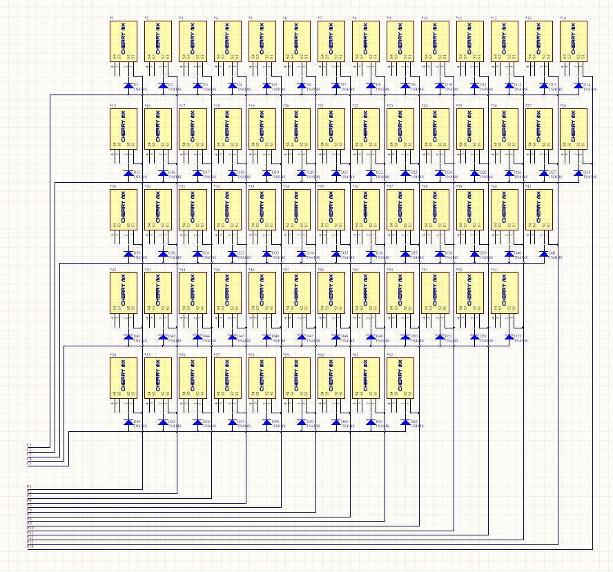
So as you probably have seen in earlier log, the schematic for the key switches is provided below:
![]()
There are 5 Rows and 14 Columns. So in total we require 19 GPIOs from the uC. I've mentioned earlier about the Keypad library. But I haven't mentioned to you why I picked this one instead of scratching to develop a new scanning techniques. Here's why:
- This library supports multi press keys out of the box. Multiple keys can be press at the same time, of course in human time scale.
- It implements state machine for every single key. From IDLE, to PRESSED, HOLD and RELEASED. it is all embedded in there.
- No Additional hardware required. As I mentioned earlier, all the unused pins are internally set to input high impedance during each scanning iteration.
- FREE. OPEN SOURCE. and more importantly it WORKS REALLY WELL. In this setup, without any loop routine interruption, just scanning. I can get more than 55.000 scanning loops per seconds. As a human trying to type 5 times per seconds is already near impossible I must say.
I owe big time to the people that have developed this library.
Alright, once you understand the hardware configuration and the hardware selection, we can go a bit deeper to the real source code itself. Well, first and foremost as you might expect, we need to define the ROW and COLUMN count in the software as shown below.
const byte ROWS = 5;
const byte COLS = 14;
Easy right. And then assign the pins accordingly to the GPIOs of the uC.byte rowPins[ROWS] = {A0, A1, A2, A3, A4}; byte colPins[COLS] = {A5, A6, A7, A8, A9, A10, A11, 22, 23, 24, 25, 26, 27, 28};That can technically be swapped around, but for the sake of readability, I assigned it the way it is connected on the schematic sheet. And up to this point, you technically have configured and matched the hardware and the software accordingly. The next step is to map, which buttons are for which. To do that, you need to assign a special lookup table. Which is nothing but a 2-dimensional constant array.char keys[ROWS][COLS] = { {KEY_ESCAPE,KEY_1,KEY_2,KEY_3,KEY_4,KEY_5,KEY_6,KEY_7,KEY_8,KEY_9,KEY_0,KEY_MINUS,KEY_EQUAL,KEY_BACKSPACE}, {KEY_TAB,KEY_Q,KEY_W,KEY_E,KEY_R,KEY_T,KEY_Y,KEY_U,KEY_I,KEY_O,KEY_P,KEY_BRACKET_LEFT,KEY_BRACKET_RIGHT,KEY_BACKSLASH}, {KEY_CAPS_LOCK,KEY_A,KEY_S,KEY_D,KEY_F,KEY_G,KEY_H,KEY_J,KEY_K,KEY_L,KEY_SEMICOLON,KEY_APOSTROPHE,KEY_RETURN,KEY_NONE}, {KEY_SHIFT_LEFT,KEY_Z,KEY_X,KEY_C,KEY_V,KEY_B,KEY_N,KEY_M,KEY_COMMA,KEY_PERIOD,KEY_SLASH,KEY_SHIFT_RIGHT,KEY_NONE,KEY_NONE}, {KEY_CONTROL_LEFT,KEY_GUI,KEY_ALT_LEFT,KEY_NONE,KEY_SPACE,KEY_NONE,KEY_DELETE,KEY_APPLICATION,KEY_CONTROL_RIGHT,KEY_NONE,KEY_NONE,KEY_NONE,KEY_NONE,KEY_NONE} };The table above depicts the correlation between the ROWS and COLS key matrix. For example, if the ROWS 0 and COLS 0 are are triggered, it then will know that the KEY_ESCAPE needs to be transmitted. And if you also notice, the table is actually arranged according the board layout for the sake of clarity.
On top of that all, as you might have spotted as well, those values inside the array above (KEY_ESCAPE, KEY_SHIFT etc) are actually a predefined constant of HID strokes. The values are the standards for a keyboard. And it can be predefined as below:
#define KEY_NONE                0x00
#define KEY_A                   0x04
#define KEY_B                   0x05
#define KEY_C                   0x06
.......
For the complete list please check this link.
So once you've got all that setup, we can start with the real application. But before that you need to initialize the library first.
Keypad kpd = Keypad (makeKeymap(keys), rowPins, colPins, ROWS, COLS);And the very simplified version of the way this works is as below:while(1){ if (kpd.getKeys()) // Check if there is any key being pressed, otherwise do nothing { for (int i=0; i<LIST_MAX; i++) // If yes, then Scan the whole key list. { if ( kpd.key[i].stateChanged ) // Then only find keys that have changed state. { switch (kpd.key[i].kstate) { // Report active key state : IDLE, PRESSED, HOLD, or RELEASED case PRESSED: msg = " PRESSED."; break; case HOLD: msg = " HOLD."; break; case RELEASED: msg = " RELEASED."; break; case IDLE: msg = " IDLE."; } Serial.print("Key "); // this prints the numerical order of the switch. Serial.print(kpd.key[i].kcode); // if uncommented, this print the character, but because HID is different with ASCII you'll see strange things. // Will cover the HID to ASCII table translation later. // Serial.print(kpd.key[i].kchar); Serial.println(msg); } } } }With very simple story and example above, I hope you can fully understand the fundamental operation of the key-mapping and scanning works for this project. Again, this library tremendously help the development of this project many thanks to the contributors.
This is just the beginning part, more to come in how to handle the multi-pressed in combination with HID modifier for sequential keystrokes.
- No additional hardware required.
-
Want to build one? HOLD ON!
08/31/2016 at 18:54 • 0 commentsIt's been pretty ecstatic looking at the comments and feedback from the community about this project. Just under 24h since it was being post in the Hackaday Blog I've discovered a lot of people trying to make one for themselves as well. Couldn't be happier. :)
However, I've also heard some comments about having a wired version of it. Also somehow version that is easier to Solder. Well I guess, I will get you covered.
I've been busy in the past couple of hours trying to reshape the current PCB design and make it "Flexible". So with the same PCB board you can either populate it as it is described so far and make it wireless, or populate it with some other parts and make it wired.
So,, Here's the plan:
Current Version (Wireless Variant)
We use AVR (Atmega2560) with the help of Bluefruit HID. Battery on the back required. SMD Solering skills required.
![]()
![]()
Proposed Wired Version (Wired Variant)
You can use the one-and-only, Teensy 3.2/3.1 board as a controller for every thing. This will cost you less Bill of Materials, and lot less complexity in the Soldering; No SMD soldering technique and tools required. But, yes, then you need to live with cable flying over your desk. See below for preview.
![]()
So, if you want to make the Wired version without worrying too much about the nitty-gritty of SMD soldering. Please hold on. I will try to post the updated Gerber by the end of this week. I will possibly order as well and giveaway some for the eager ones :)![]()
-
Thanks Brian!
08/30/2016 at 11:01 • 0 commentsAin't no better morning than having to read your "thing" being featured on Hackaday Blog. Many thanks to Brian @Benchoff for the amazing post ! :)
![]()
-
fSociety Workstation
08/27/2016 at 11:58 • 4 commentsI think I haven't mentioned it anywhere else before about this.
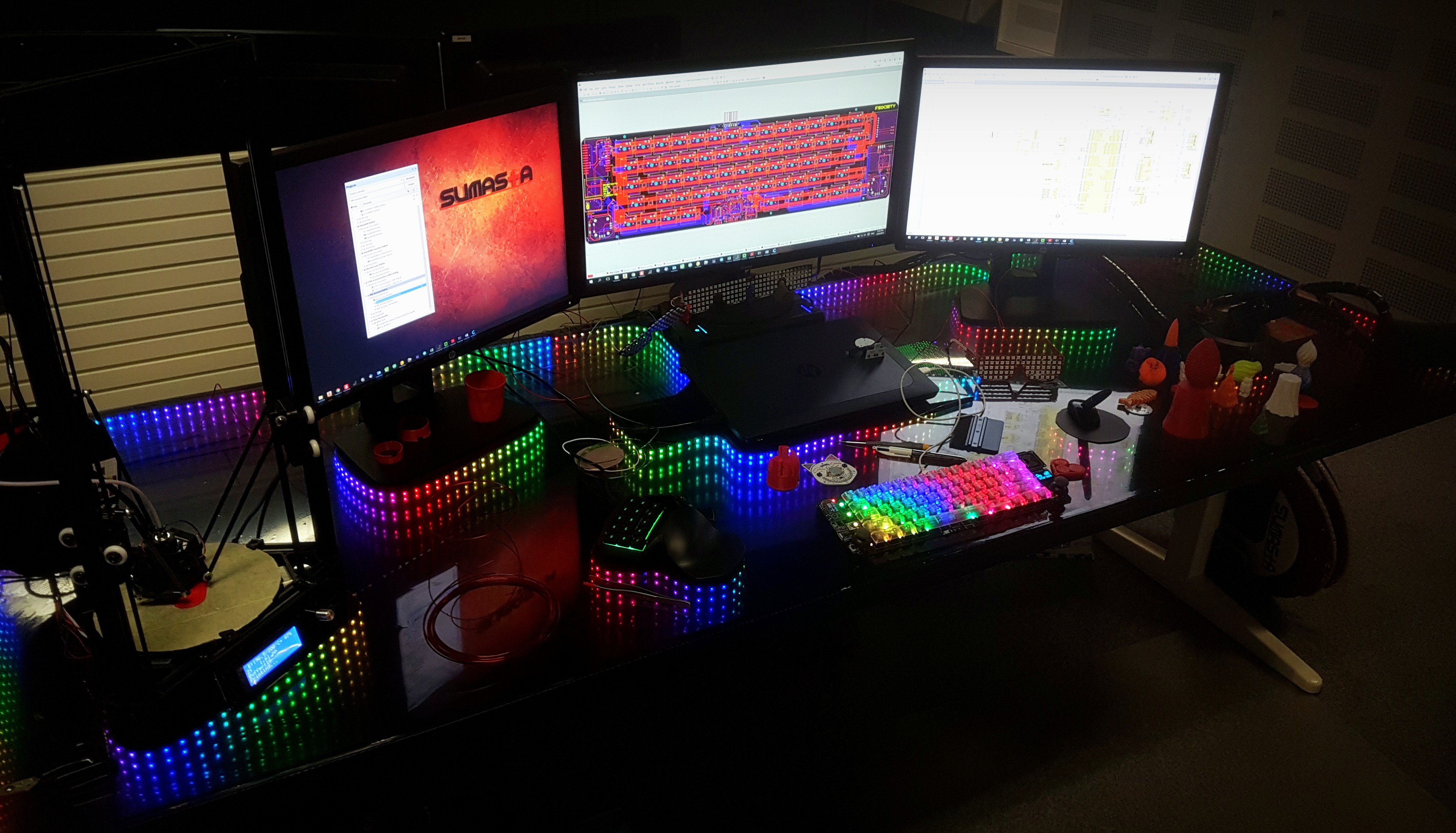
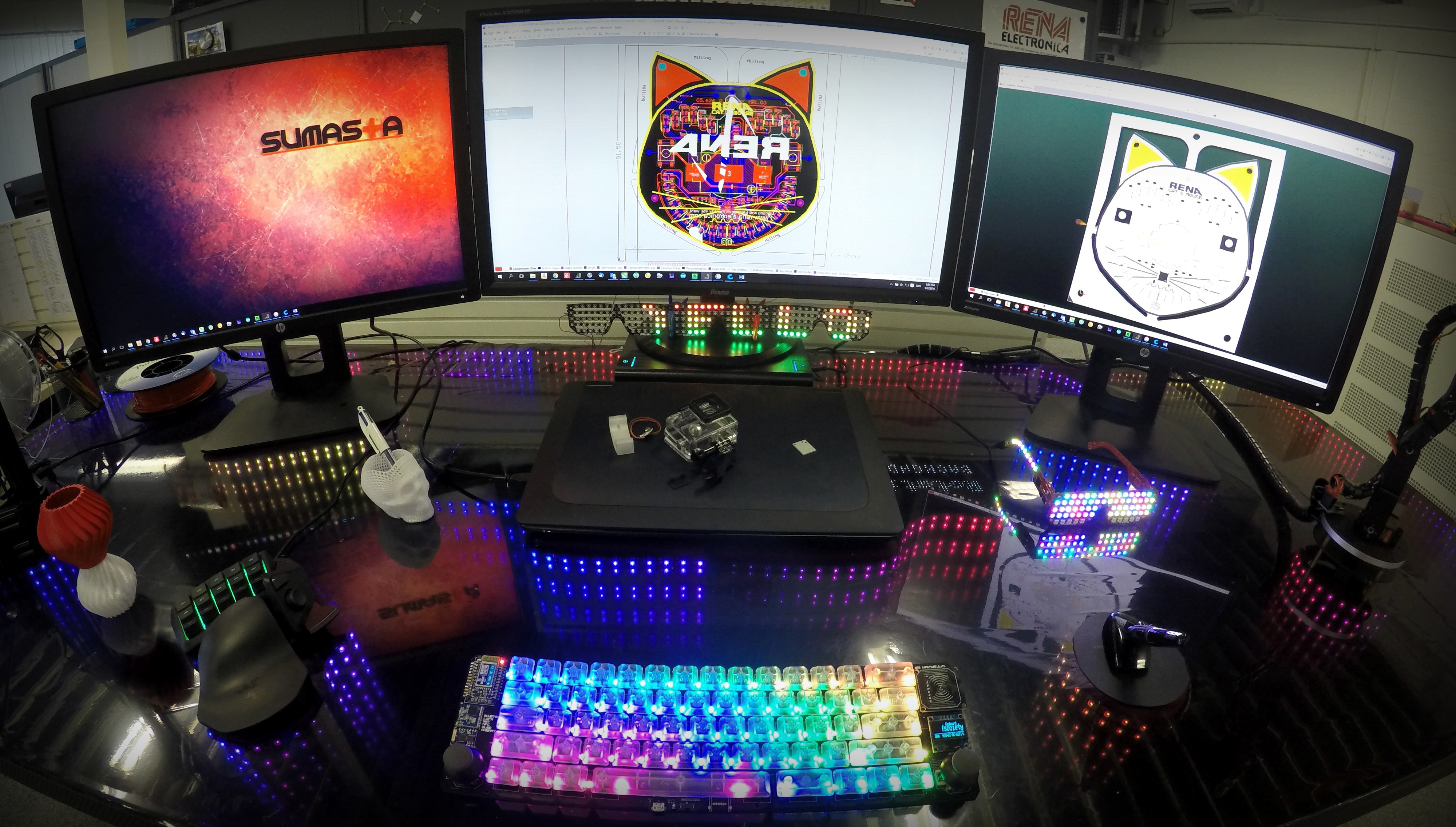
One of the main reason behind the creation of the fsociety keyboard is that I was planning to build a workstation as well. Reason is simple, I spend around 15 hours a day in the office almost everyday. I guess then my desk deserves some funky adjustment and some sort of master terminal control.
Below are some pictures after quite heavy works during my "vacation days" couple weeks back:
![]()
As you probably have spotted, There are:
- 3D printer on the left hand side
- 6-DOF robotic arm on the right hand side
- Bunch of LED matrix in the front side
- And of course, >1000 Ws2812b attached in and on the desk.
- Ohh also the Infinity mirror as well :)
- More to come!!!!
And guess what??
Because of fsociety Keyboard, I have full direct control of things that are around me; beneath a palm of my hands, in a single click, effective immediately.
I think I need to make another project page for the building process of the workstation as well (?) ^.^
-
Assembly
08/22/2016 at 22:50 • 0 commentsAs I probably have said on earlier log, I started this project 3-Weeks ago with no intention in mind at all to post the documentation online and let alone submitting to Hackaday Prize contest. I started posting this project from nothing just two days before the due dates of the Automation contest. 4-build logs in less than 24 hours ;) I consider myself to be a pretty good last-minuter.
Having said that, during the build time, I was just too excited in getting it done instead of taking pictures in every single build step. Well, I kinda regret it now. Even then, luckily there were still some pictures I made along the way.
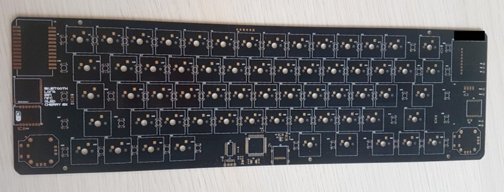
Check the incoming PCB
First thing as always, start with the bare PCB. Not all the PCB you receive have the same production quality. Check things like Sharpness of the silkscreen, scratch, the bending ratio etc. If you order 10-pcs, typically you'll notice that one or two boards just slightly better than the other.
![]()
Start with a 'remote' components
Assembling manually something like this need quite a bit of attention, even before grabbing your soldering iron. You have to understand whether in the finished board, this & that particular components are reachable and fixable. If you're onlu dealing with SMT part, normally that's not a big deal, but if you start using Though hole components like the one I use here (Cherry MX), you might need to step back a little bit and decide which one to go first.
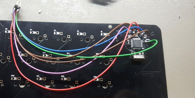
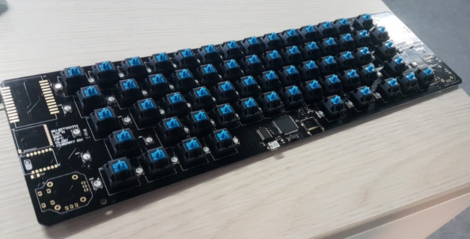
And In this case, it is pretty obvious that you need to solder the WS2812b RGB Leds first. Because once you soldered all the Cherry mx switches, it is simply impossible to solder the LED. Even repairing it is already hard enough without de-soldering the neighboring switches. Well, but wait, while you solder, you can simply just power it up to check if the Cherry mx is working. It needs uC to light up the LED. And as I mentioned on other log, there is a dedicated uC that handles the LED and it located on the bottom side of the PCB.
So the plan was simply to solder the circuitry for the uC, test and flash it with WS2812B demo software, then you can just begin to solder the LED Array.
(Excuse the flying wire on the picture above. I didn't add 6-icsp pin on board.) Well then once you manage to program the ATMEGA328p, next step was to solder the LED on the top side.![]()
Solder it one by one, until the whole PCB is surrounded by WS1812b RGB led and Voilaa!![]()
Make sure you are gaining some 'blessing' from the colorful LED before proceeding. But before proceeding, some more stress or bend test might need to be done. Because well, if you happen to solder the WS2812b not well enough, there is a chance that it stops working after you use and type with the keyboard many times. And remember, because of the placement, it is going to be a hard job to fix.
Moving on from the LED, it is time to proceed to more challenging stuff. Yes, soldering the fine pitch components. Primarily in the beginning you only need to solder the ATMEGA2560, the crystal + caps, micro usb for power and wire for programming, that's it. Once you manage to program it through SPI and put bootloader in it, you can then proceed to solder the FTDI FT232RL for programming it through serial.
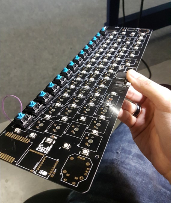
Once that's done, it is then the time to handle the most exciting part. well yes, the soldering of the Cherry MX. Technically speaking, this is the easier part of all. Cherry MX is a through hole components and I happen to make well enough footprint library. Inserting and soldering the switches was very convenient. See photo below.
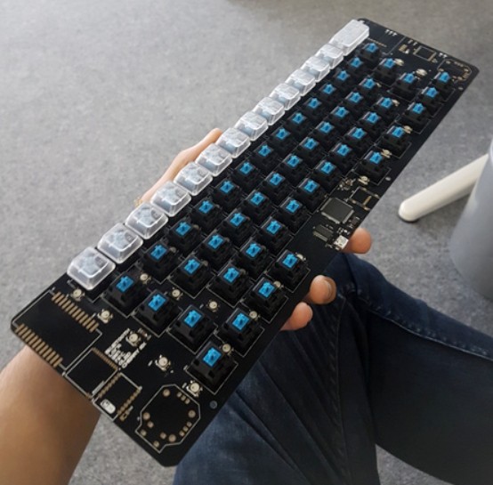
Piece by piece, then an hour later it started to appear like a keyboard.![]()
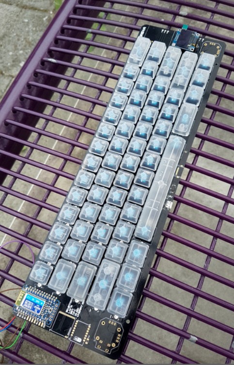
And from this point one, you can already try placing the keycaps for the keyboard if you want. Or finish soldering all the modules on both ends. For me I did put all the keycaps first to see how the RGB color diffuses on the keycaps.![]()
Once you finish putting the keycaps and solder the Bluefruit module. you are pretty much ready to tweak around the software just as a basic keyboard.![]()
![]()
The rest of the module was soldered the following days and I didn't have enough motivation to take a picture of those. but well, in the end it should be something like you see below.
![]() Thanks for reading !
Thanks for reading ! -
The fboardLayout
08/21/2016 at 17:33 • 0 commentsYou've probably have enough with the schematic layout in the previous log. It is now the time for the more interesting stuff; The board layout. I've spent the whole weekend to finish this design from making the library, schematic and then lastly layout. Of course, didn't have time to do grocery or even shower during that weekend ;) Even with the rush, I've noticed that I made only one mistake. I swap the VCC and GND in the OLED library. oops. Apart from that is hunky-dory. Below just a preview of the final board design before I explain in more detail about the design choice etc.
![]()
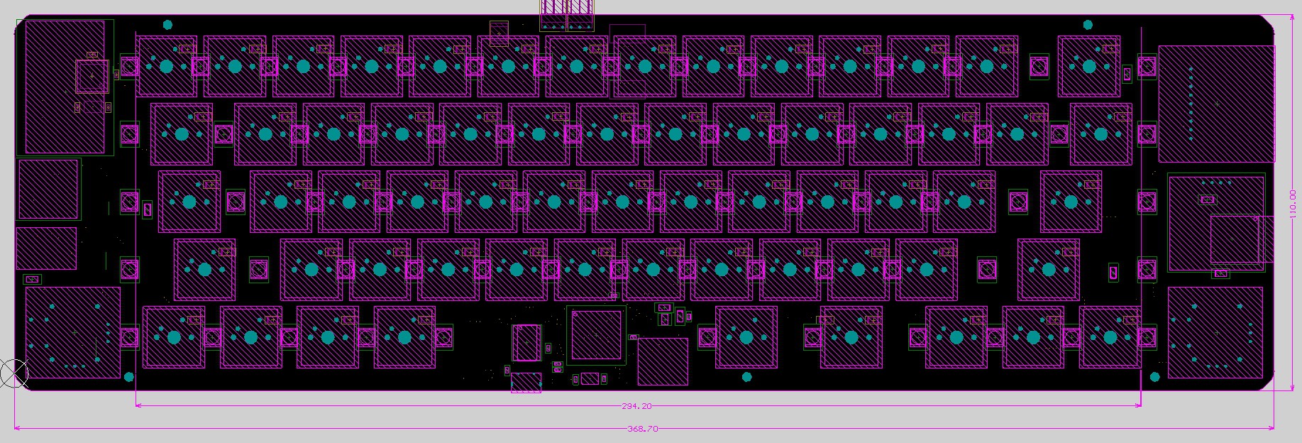
Board Dimension
This was very important in the beginning. I started in the beginning by placing all the cherry mx switch in place with 2mm distance between its widest part. I figured that 300 mm in length should fit all the cherry mx keycaps, but that still excluding other components. all the modules can be placed on the bottom side, but the Joysticks are not possible. it just has to be on the top. like it or not, adding around 33 mm on each side should suffice the space requirements. Initially I was planning to round the length to 400 mm just to make it easy and have some room space for some improvisation later on, but the cost for the PCB compare to 368 mm is significantly quite high. Therefore I stick with 368 mm.
![]()
Next thing is about the width, 100 mm sounds like a good round numbers right? Well not really it is only later you realize that you will need some extra width for the array of traces on the bottom side of the board. I decided to add 10 mm to the board width. And needless to say, aesthetically, with 100 mm width, and the tall keycaps, the board looks a bit clumsy. Having some spare width tremendously help the visual side of it. trust me.
![]()
Placement & Routing Concept
As I mentioned in earlier Log. I just don't like asymmetry. So since the beginning, I always stay conscious to spread the components evenly. It concludes to several points listed below:
- The main Microcontroller unit is located in the center of the board. not on either side. It is very importat for the sake of the routing. And if you want to stick with 2-layer board as well. I just simply cannot think that it is possible to route the board with 2-layer if you locate the primary Atmega on either side. The routing of the matrix of the switches will easily become a nightmare.
- The primary keyboard is centralized. It has to be the center and the main attention of the board. Unlike most keyboard, the keypad on the right ruins the potential symmetry of a keyboard as a whole.
- One joystick on each side. Instead of having two on the right side for Arrow as well as the mouse. One has to be on the left side and another one on the right side.
- NFC/RFID Reader has to be on the right side. Well yes, because I wear the right on my right hand ;)
- The rest of the modules evenly scattered on the right and left side of the board. And only on the top side. And of course, watch out the cross-talk or some black magic voodoo happening between the antennas. (Need RF guy here to comment)
- WS2812b placed between the Cherry MX switch and the co processor has to be placed on the bottom side. it was simply because there was no room on the top side anymore.
Now that We have the concepts nicely described on a bullet points above. I give you a tour through the design in 3-Dimension concept. Needless to say, this is one of the perks in using Altium.
![]()
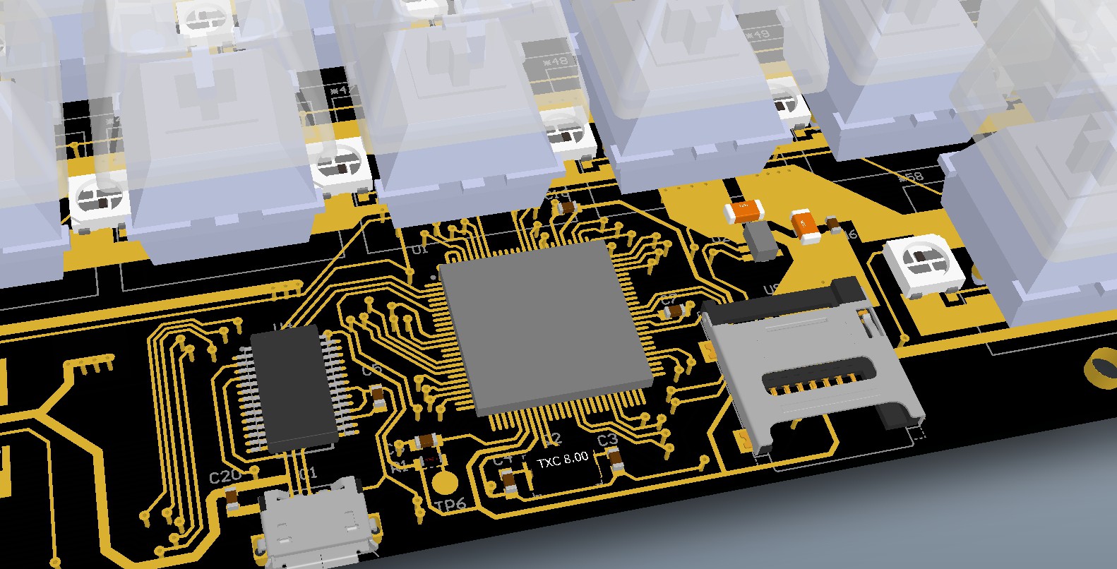
Main Microcontroller ATMEGA2560
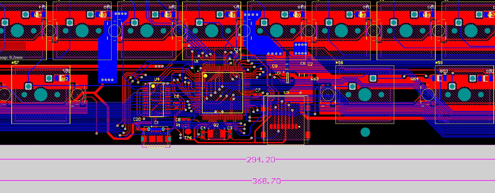
The microcontroller as you see above is located in the bottom center of the PCB. hiding safely in underneath the space button. (FYI I didn't have a step file of any other keycaps except the standard one). It was quite a fortunate thing to have such a empty space just on the spot where I needed. If you lok at the picture below, all the Row and columns from the key matrix can be routed easily. Making it more like a star topology. Don't forget it is not just for the sake of routing the switch matrix, but also all other peripherals on either side of the board. On the second picture below you can see all the communication bus propagates to either side equally. I strongly believe this was a good design choice. Moreover, the USB connector you see below is for programming and debugging purpose.
![]()
![]() The Switches array & the LED
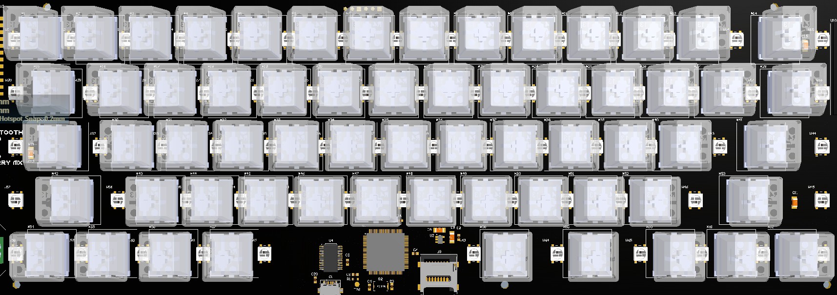
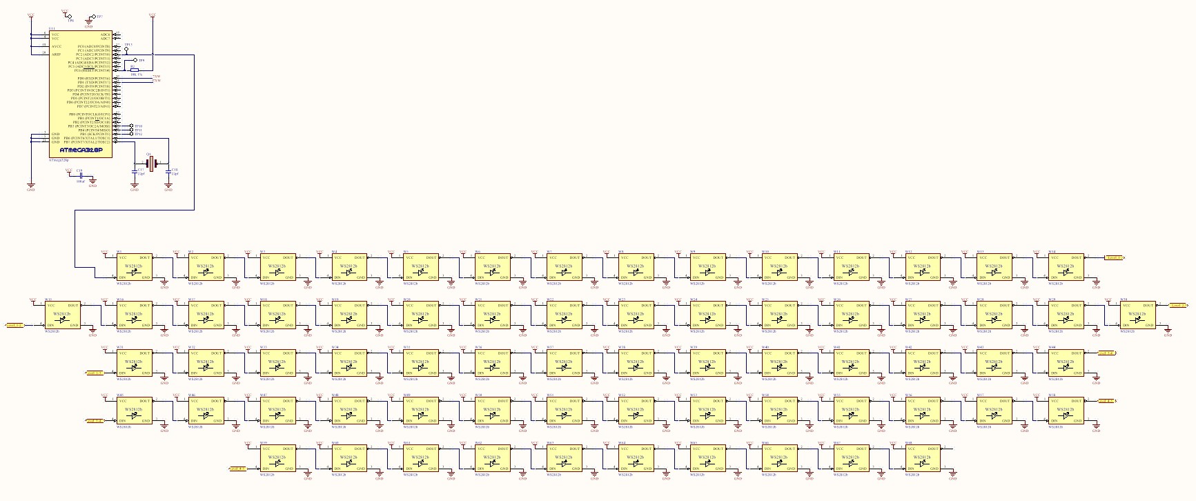
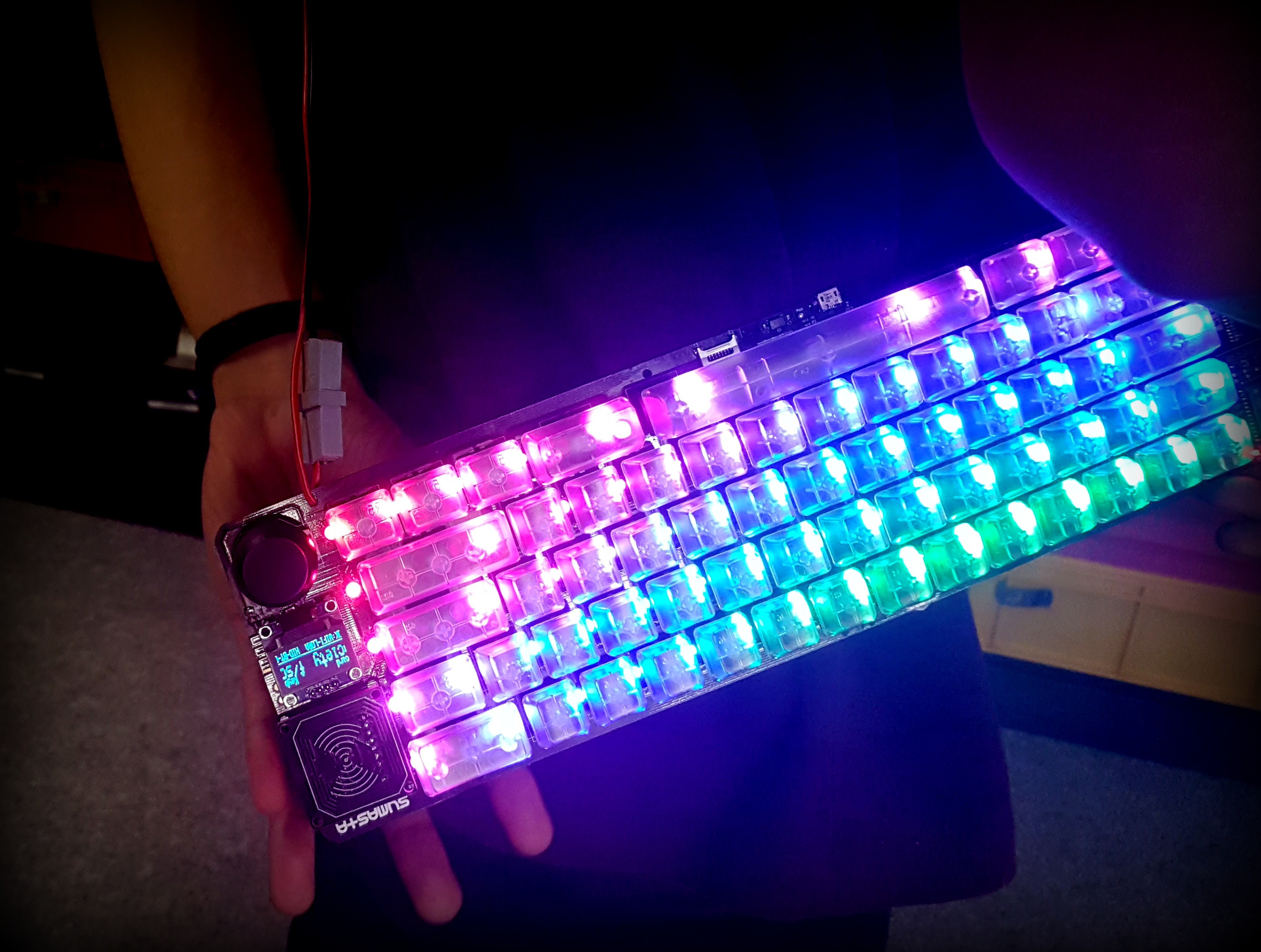
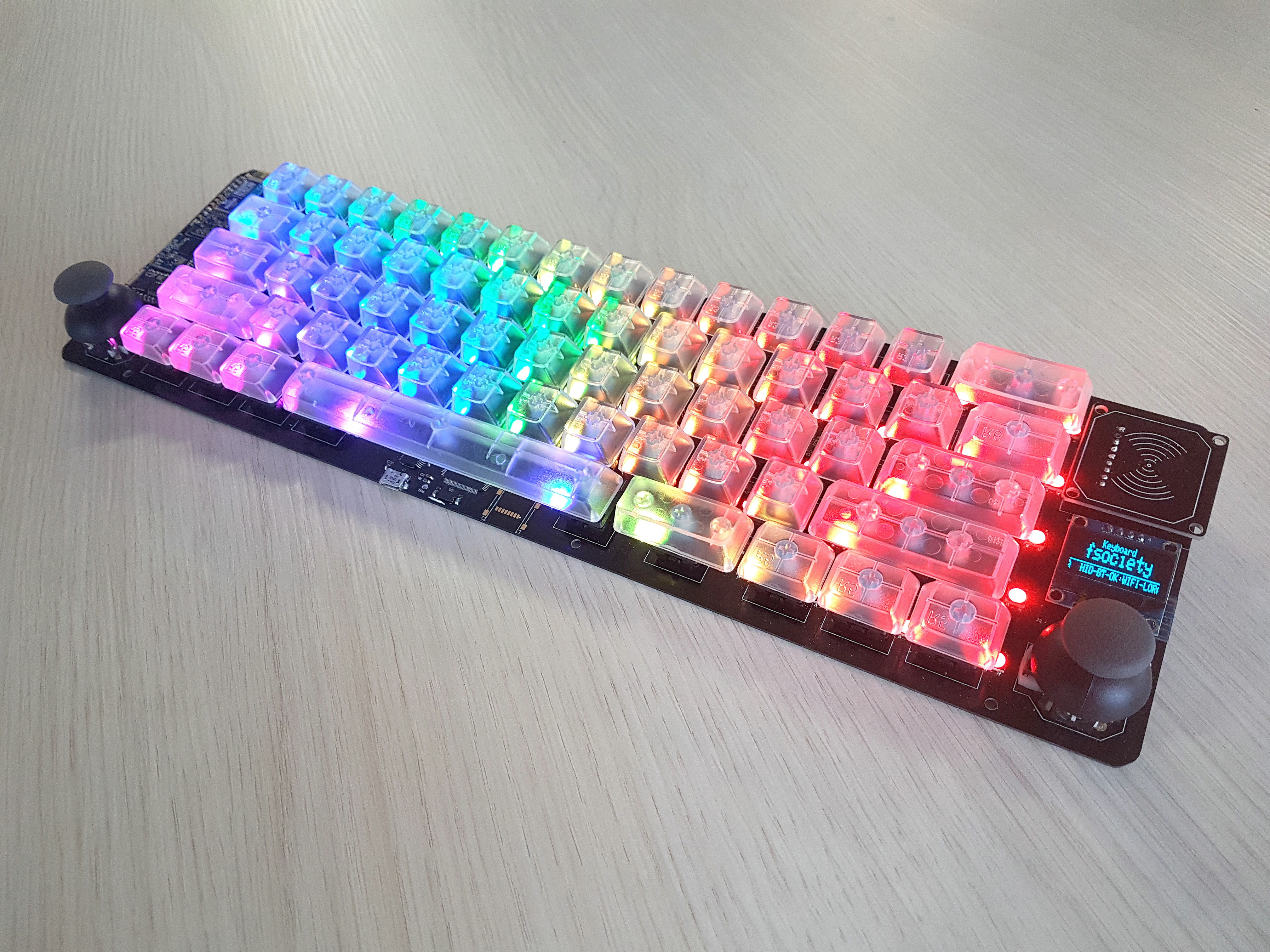
The Switches array & the LEDThere are 62 Cherry MX on-board that are surrounded by 68 WS2812b RGB Led. The final result shows as follow:
![]()
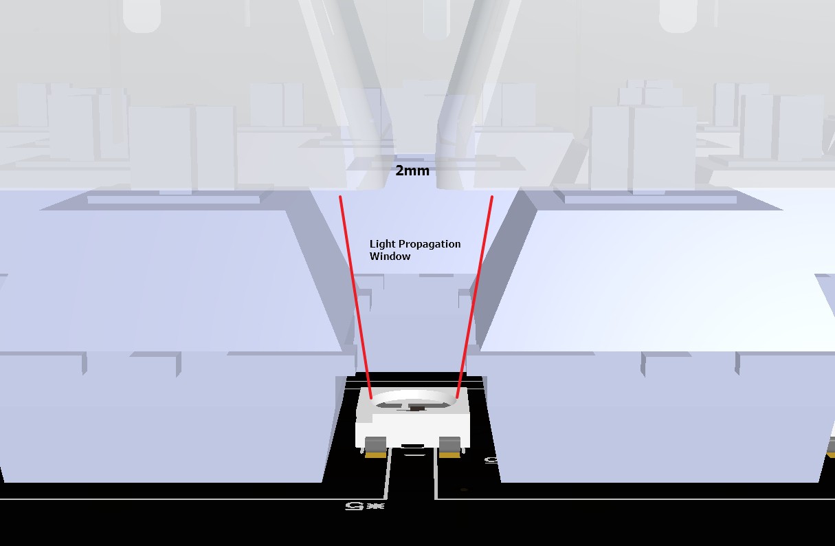
The challenge was quite simple but was a bit tricky as well. I had to find just enough spacing between the keycaps that is not too big and not too small allowing the Light from WS2812b to pass through while not sacrificing the typing ergonomic. Also at that time, I just haven't got a clue what was the tolerant of the Chinese transparent keycap. Having it too narrow posses quite some risks. Moreover I simply couldn't get the best out of the ideal light propagation angle from the WS2812b for typing-ergonomic.
However, following some prototype printed on a piece of paper, it seems that 2mm clearance between the keycap will be good enough. It will still be comfortable for typing yet also the light propagation windows doesn't get too narrow. In the future, I will definitely use the family series of Cherry mx switch that has transparent housing instead of the boring-black.
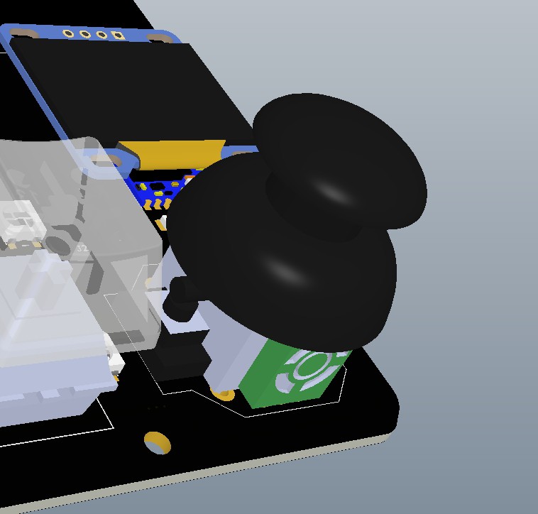
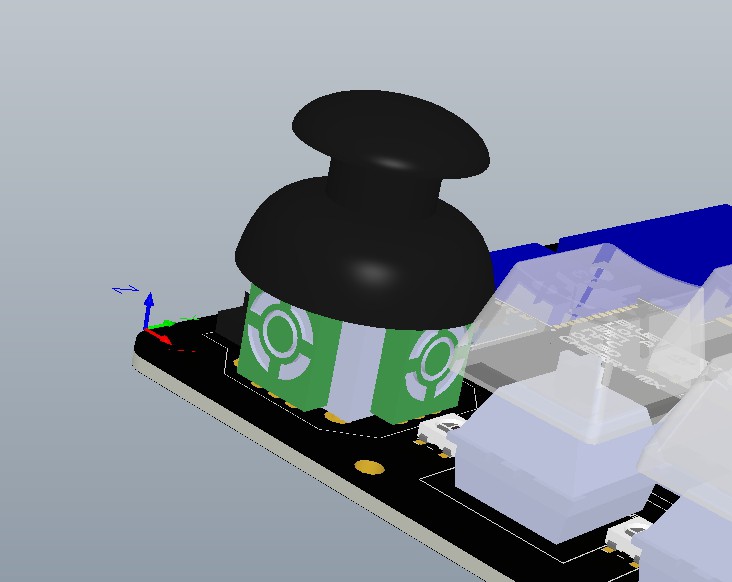
![]() One Thumb Joystick on each side
One Thumb Joystick on each sideYup. I don't think that is bad idea after all. I could've put both joystick on the right side because I'm right handed. But then I won't have space for the NFC tag on the right side. So having in on either side sounds like the best options. The right one for arrow buttons while the left one is for the mouse movement.
![]()
![]()
NFC/RFID Reader on the Right hand side
For obvious reason, I use NFC ring on my right hand fingers, so obviously no question where I should place it. Interestingly enough this particular module has antenna that is on the other side of the primary component side. So once mounted on the primary keyboard, you only see the logo of the antenna and that's it.
![]()
The rest of the Modules
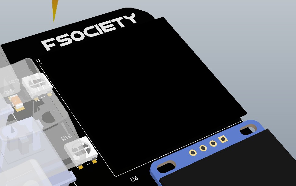
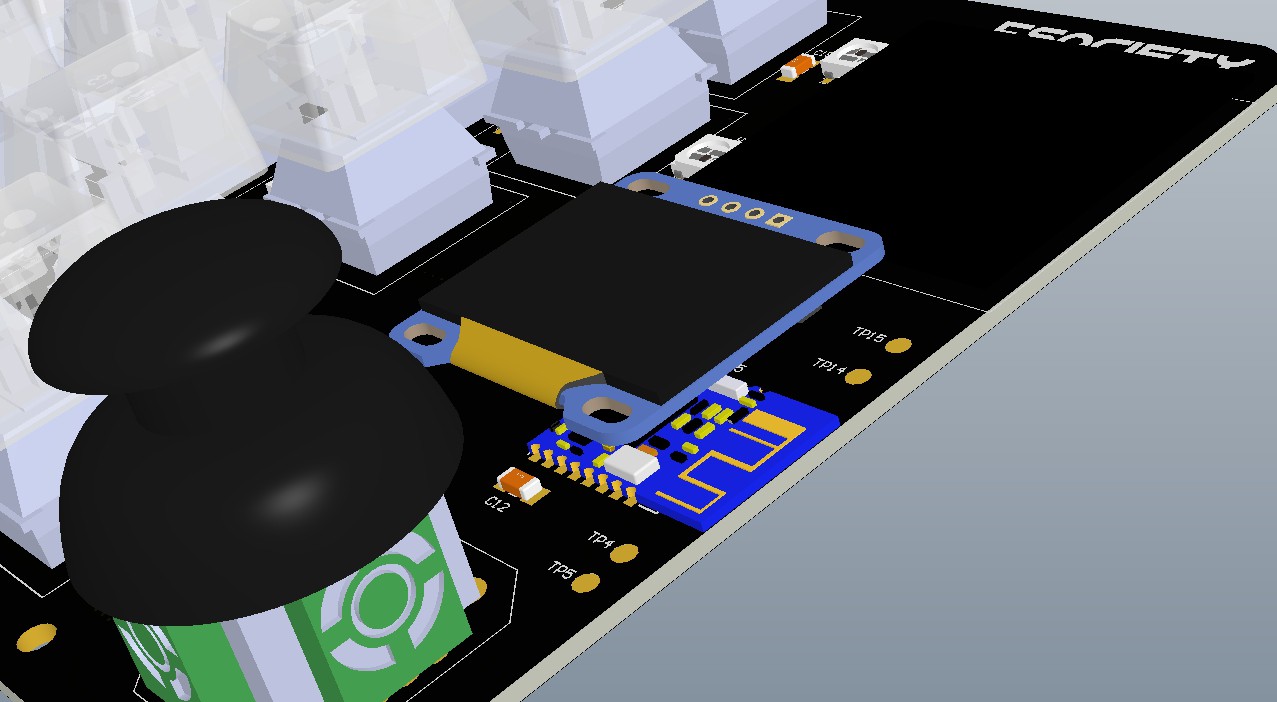
Started from the right hand side. There are two more modules that hasn't been covered yet. And those are the OLED and the Bluetooth 4.0. The tiny bluetooth module hid underneath the mini OLED display as depicted on the picture below. So far it didn't quite give any performance issue regarding the wireless transmission etc.
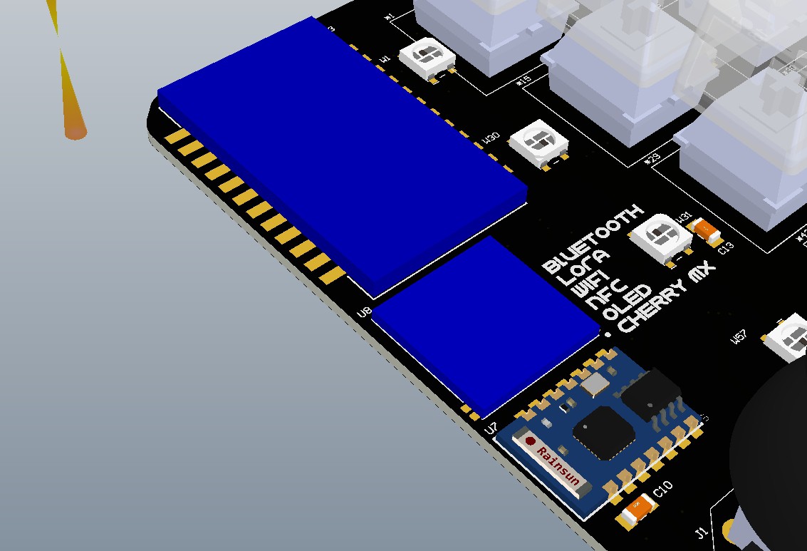
![]() Moving on to the left side. There are three modules that is placed next to each other as can be seen on the picture below. The biggest blue rectangle on the top is the Bluefruit HID (couldn't find a .STEP file for it unfortunately) while the blue in the middle is the LORA module, and the lowest one as you'd probably have known is the ESP8266 module. Bluefruit HID and the ESP8266 Wifi module talks in 2.4Ghz while the LORA is sub 1Ghz. Haven't test much the transmission performance of the antenna up to this point. However, the Bluefruit HID and the ESP8266 seems to work just fine.
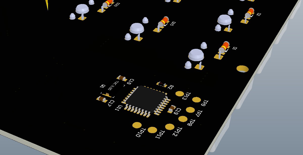
Moving on to the left side. There are three modules that is placed next to each other as can be seen on the picture below. The biggest blue rectangle on the top is the Bluefruit HID (couldn't find a .STEP file for it unfortunately) while the blue in the middle is the LORA module, and the lowest one as you'd probably have known is the ESP8266 module. Bluefruit HID and the ESP8266 Wifi module talks in 2.4Ghz while the LORA is sub 1Ghz. Haven't test much the transmission performance of the antenna up to this point. However, the Bluefruit HID and the ESP8266 seems to work just fine. ![]() The Co-processor aka the LED Driver
The Co-processor aka the LED DriverThere isn't much happening on the bottom side quite frankly. Only the dedicated LED driver which is the ATMEGA328p that is located on the bottom. Also diodes that was replaced by resistor in the final assembly.
![]()
Well, that was it. You can file on the project documents or here the 3D adobe PDF file of the design. What you need is only a Adobe Acrobat reader ad have fun browsing through the design.
-
The fschematic
08/21/2016 at 15:20 • 1 commentIt is going to be in Altium, yes Altium Designer. I repeat Altium, not Eagle sorry.
I've had enough amazing time using Eagle for more than 6 years since 2009. only until the beginning of 2016 I started to use Altium Designer as my current job mandates. And you know what? I felt like my whole life in designing PCB prior to using Altium Designer seems more like a lie. The easy way to put this is just like when you always use Paint to adjust and modify some image and in all the sudden someone introduce you about Photoshop. But well, I do agree that the learning curve is a bit steep with Altium, but I had to say it was worth the time.
I do also understand that Eagle is nowadays a common tools within Maker Community, so using tools other than Eagle might give some disadvantage for many. Either way, I was simply just cannot move away from using Altium at this stage, especially considering the limited time that I had etc. Also in the future I will try to see if I can properly export the Altium design files to CircuitMaker. which is a strip-down version of Altium Designer that is free and online/community based.
Schematic Section
During the design process I separated the design into three different schematic schematic sheet. Not just for readability, but also one of the sheet was a import from my previous project. So well, there is no reason not to do it.
Cherry MX Matrix switches
First and foremost is the Matrix of Cherry MX switches. It is fairly straight-forward, just an array of 14x5 switches connected directly to the pin of the Microcontroller. Though you see a diode on the schematic below, in the end I decided to replace it with just a resistor. Because the potential crosstalk between switches can be handled inside the software by setting the irrelevant pin to high impedance in every scanning iteration. So no diode is really necessary.
Another thing to note also you might find the last row (R14) to be unnecessary. The two switches can be hooked up to Column five (C5) and that way you can save one pin from the Microcontroller. But well, I didn't do it. simply i was trying to avoid un-uniform-ity in the routing. If you take a closer look, the number of switches per column in the schematic is identical with the number of switches per column on the board layout that we'll discuss in the next Project logs. I thought it could ease the mapping process in the software in latter stage.
![Fsociet_Keyboard_Cherry]()
Next thing to discuss is the array of the WS2812b RGB Led, the one and only favorite. Exactly 68 pieces of those were used to nicely fill the gap between the switches. As you might have known, the beauty of this LED is that you only need one microcontroller pin to sequentially control hundreds or even thousands of this LED. So schematic wise, it was not that difficult. But as I briefly mentioned in previous project log, I might actually need a co-processor to control the LED smoothly without being interrupted to much with other primary routine. Hence, in the schematic below you see an Atmega328p microcontroller as well.
Primary peripherals
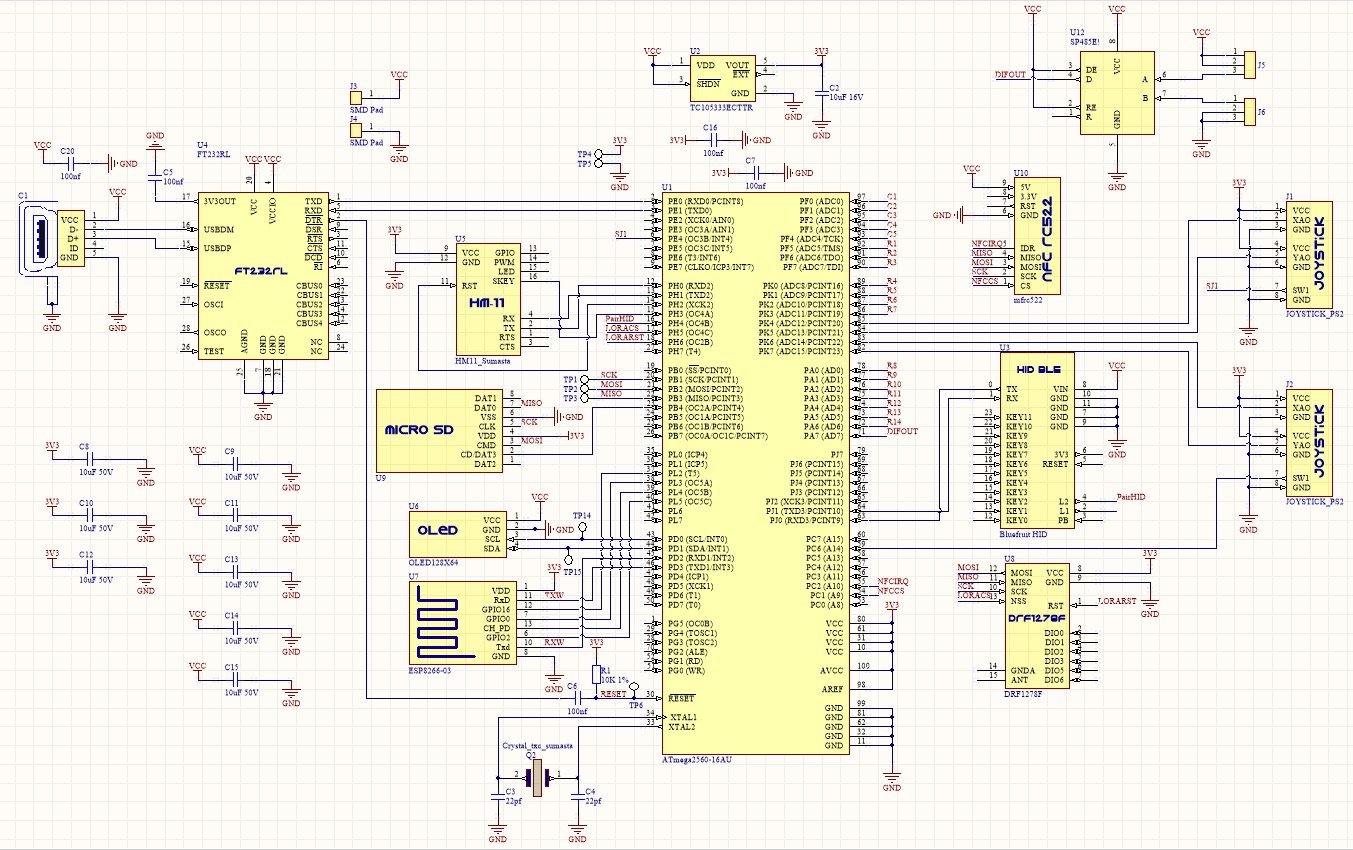
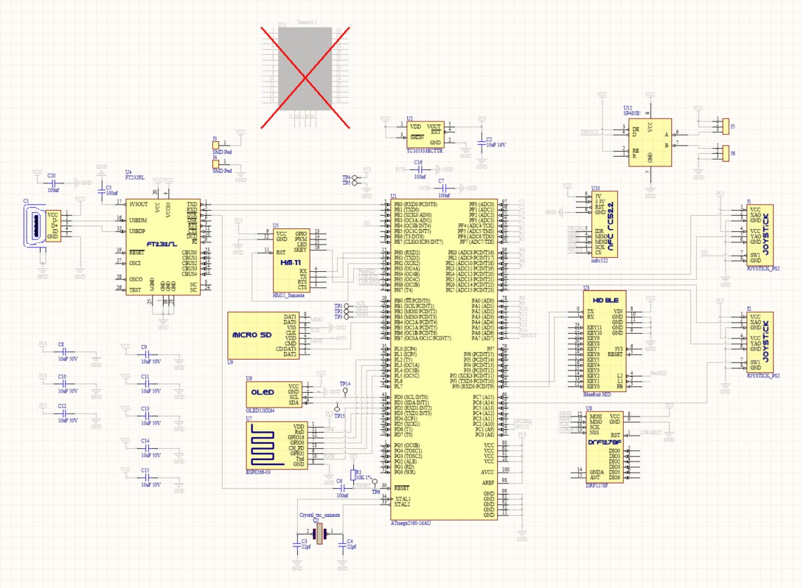
Well, following the above, it is now time to get into more serious stuff. The primary controller and the peripherals itself. The schematic provided below depicts in great detail the complete wiring diagram of the system. All the standard communication bus are occupied although there are still some free pins for additional features in the next design iteration.
In summary, started on the left side is the standard FTDI IC both for debugging and programming. Taking the most space in the center, that is the main processor itself ATMEGA2560. The Bluefruit EZ key, ESP8266, FT232RL and HM-11 occupy all the Hardware serial port. While DRF1278, MRC522 and the MicroSD card shared the same SPI bus. On top of that, the OLED is the only one connected to the I2C bus. Joysticks on the other hand connect to 4 analog pins available on the microcontroller.
And that was it. It was quite straight forward overall. The time was a lot more spend on making the Altium library for most of the modules and components. Quite frankly that's what I often don't like in using Altium, every single time a unique components/modules is used, there is a great chance that I have to generate the library myself. Well, you know in eagle, most of the time someone else have made the part you need for you.
The fsociety Keyboard
(Mr.Robot's) fsociety inspired Mechanical keyboard. Wirelessly sense, assist and automate your good and bad computing activity.
 Pamungkas Sumasta




 Thanks for reading !

 The Switches array & the LED