Close
0%
0%

Printem - Instant Printed Circuit Boards

A novelmulti-layer film that lets you quickly and easily make flexible copper PCBs all using normal, unmodified home printers

Similar projects worth following
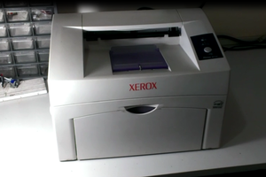
The goal of Printem was to create a way for anyone interested in electronics to be able to quickly prototype and iterate using Printed Circuit Boards (PCB). Printem does to the creation of PCBs what Polaroid did to photography. To create circuits, all you would need is the "Printem Film" and any unmodified home office printer with normal ink.
1) Print your circuit pattern onto the Printem Film
2) Expose to UV
3) Peel to reveal copper PCB

Why did we start on this Project ?

As researchers who work day and night with hardware and an avid electronics enthusiasts. We were looking for an alternative to existing PCB prototyping methods. Sending boards to a fab house either takes too long or is too expensive. Conductive Ink Printers, Milling Machines etc all need one to buy special equipment and etching PCBs yourself is a multi step process and is kind of messy. Thats why we created Printem.

You can see it in action here


How it works and the various design consideration and materials of the Printem film will be describe in the project logs. So stay tuned !

We have built a proof of concept system to show that it works, the goal now is to improve the resolution and usability of the Printem Film and involve the community to make a truly useful rapid fabrication tool for electronics prototyping. We would love to hear your thoughts and opinions !

Looking forward to all your comments, critique, suggestions and advice !

Cheers!

  • Some samples made with Printem

    varunperumal08/23/2016 at 00:07 0 comments

    This video should detail a bunch of sample made with the Printem film

    We are in the process of creating more build logs and detailed instructions for people to create and try out some films, we also have a bunch of samples that we made for testing, will be glad to send them to anyone interested as well.

  • How the Printem Film works ?

    varunperumal08/23/2016 at 00:04 0 comments

    It is recommended that you follow the project logs in chronological order.

    So how does the Printem Film work ? It uses the selective adhesion of the copper to the substrate using the UV adhesive to "tear away" only the copper in the right places to form the circuit. The diagram below illustrates this

    a) The home/office printer prints black ink onto the acetate substrate, the PCB pattern is printed in negative, meaning that only the areas with the copper traces are left transparent and everything else is printed on .

    b) When this is exposed to UV light, the printed ink blocks it from passing through, so only areas without the ink allow the UV light to pass through. The light then passes through the substrate ( which is UV transparent ) and cures the UV adhesive only in the areas directly underneath the unprinted areas.

    When the UV adhesive cures in response to this exposure, it strongly adheres to the copper foil below it

    c) When the layer is peeled away, it "pulls" only the desired copper with it, leaving the rest attached to the peel-off layer and then being discarded.

    d) Now the PCB is ready to be used

    The next post details some examples made with Printem

  • Construction of the Printem Film

    varunperumal08/22/2016 at 23:52 0 comments

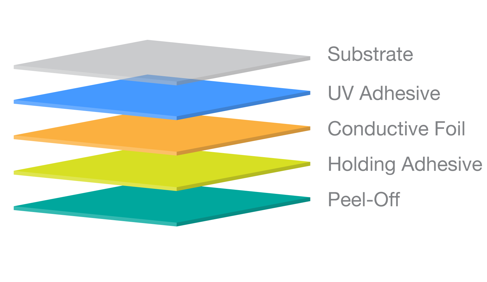
    The Printem Film is a self contained film that contains all the materials necessary for the creation of a copper PCB. In the current version, the Printem Film has 5 layers as show below

    This is a brief description of the stack, for more detailed look, please wait for more project logs or you can also read the full paper here

    1) The substrate is made of Acetate paper, the kind you use to print slides on for old style overhead projects, this is what the PCB will be finally formed on ( currently working on using a high temperature resistant alternative )

    2) Then we coat this substrate with a UV curing adhesive, these adhesives basically bond and activate when exposed to UV light, this is the active component of the Printem Film

    3) Then we have the conductive foil, in our case this is a copper foil bought from a crafts store, silver, gold and tin foils can also be used as long as they are thin enough, we are looking for a similar thickness as to the decorative gold foils you find in craft supplies

    4) The holding adhesive basically holds the above layers to the peel off layer below . This has to be an adhesive that is strong enough to hold the stack together but weaker than the UV adhesive in its cured state ( More details to follow in the posts to come )

    5) Finally the peel of layer is simple card sock that is thick enough to block light

    All the layers above are arranged in the order as show and put through a roller press to bond them together into a single sheet. Once the sheet has been formed its ready for use. This seems like a lot of work to do. But the vision is that you will be able to buy sheets of Printem Film and use them without having to go through any of the above steps.

    The next log will go into how all the above materials work together to create the final result.

  • Using Printem

    varunperumal08/22/2016 at 23:32 0 comments

    The goal of Printem is to let anyone easily, quickly and cheaply create Printed Circuit Boards for prototyping use. Imagine if one could create single layer, copper PCBs in less than 2mins after you design them, one will be able to quickly test and iterate on the designs, we believe that Printem is a useful tool for anyone who works with electronics and hardware.

    So No Etching ! , No Special Inks !, No Special Equipment ! All you need is the Printem Film and a normal home office printer.

    The build logs goes into how an end user would use Printem, this will be followed by posts on how the Printem film works, how to make your own and the current work that is being done on improving its various attributes. We would love to hear your thoughts on how useful Printem might be in your daily work.


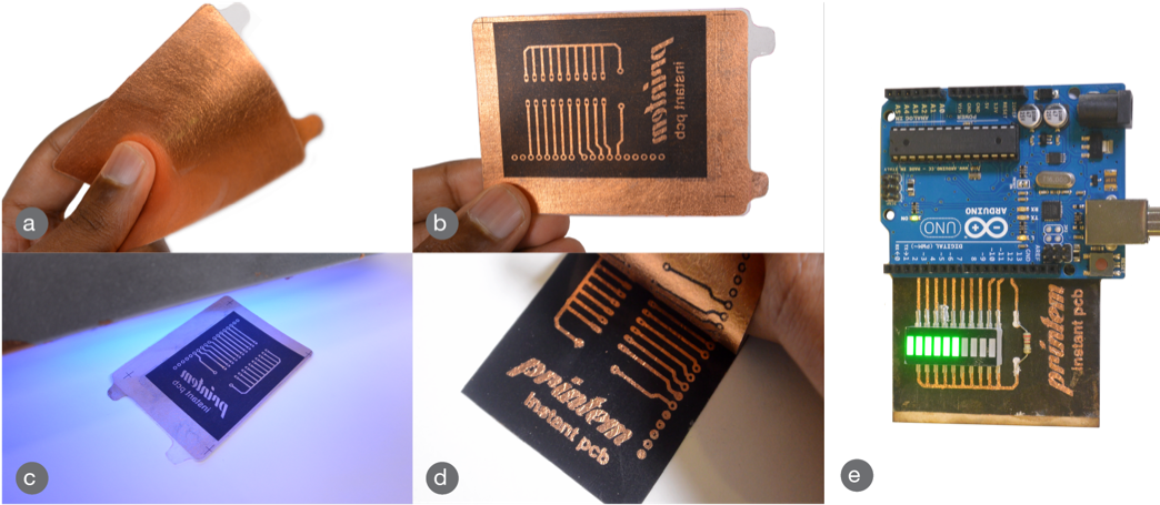
    a) The key to Printem is the Printem Film - which i s a multilayer stack of materials that work together to produce the final copper PCB

    b) The circuit pattern is printed on the Printem Film using any laser or inkjet printer using black ink

    c) The film is then exposed to UV light or sunlight for 30 seconds ( or lesser if the light is intense )

    d) The top layer is peeled off , revealing the copper PCB underneath, this is ready to use

    e) This just shows a simple LED bar graph being interfaced with an Arduino.

    All this only takes about 2 mins !

View all 4 project logs

Enjoy this project?

Share

Discussions

Kris Keillor wrote 08/13/2024 at 04:22 point

really fantastic idea... any progress on developing it for a wider release?

  Are you sure? yes | no

Ember Leona wrote 10/08/2018 at 06:03 point

SofaKing Cool! Kick AWESome! If its affordable. I had an idea of laminating ground up copper and trying to make a coppertoner or using magnet wire on sticky side to move out lines. But your idea looks better maybe not cheaper though. openInvent.club

  Are you sure? yes | no

Ron Smith wrote 07/07/2017 at 15:50 point

Fantastic!  Where/when can I get some?

  Are you sure? yes | no

yogdabade wrote 08/29/2016 at 12:45 point

Hey, Its Really a amazing tech , when it be out for commercial , Will it be for available for multi-layer  printing? 

  Are you sure? yes | no

varunperumal wrote 08/25/2016 at 03:51 point

Thank you everyone for your encouraging comments ! We will definitely keep you posted as this project progresses.

  Are you sure? yes | no

Troels wrote 08/24/2016 at 14:23 point

Where's the Kickstarter project? This looks really cool and I'd be really happy to try it out :)

  Are you sure? yes | no

RocketGuy wrote 08/24/2016 at 14:03 point

+1 for a kapton version.  Looking forward to seeing this hit market!  

  Are you sure? yes | no

zakqwy wrote 08/23/2016 at 20:03 point

Seems like a neat and promising technology. What feature size can you hit? What's the planned cost target for a given amount of the film? What's the temp limitation for soldering?

  Are you sure? yes | no

varunperumal wrote 08/24/2016 at 06:15 point

We are working at about 24 mils traces with 24 mil spacing right now, thats probably not very useful for any circuit that is moderately complex. ( Pictures and making instruction soon to be updated )So we are testing several improvements to bring it down to 10mil traces with 10 mil spacing. 

Regarding the temperature, the examples show in the video (except for the paper speaker one) are made on acetate substrates, so they will not withstand soldering, but the paper speaker uses a colorless kapton substrate and a higher temperature resistant uv adhesive that we are still testing. Those can withstand up-to 400F for soldering and reflow purposes

  Are you sure? yes | no

zakqwy wrote 08/24/2016 at 15:47 point

Thanks for the detailed reply. 24mil is a bit big for some fine pitch stuff, but it'd still be useful for prototyping. Good luck, this is an awesome project!

  Are you sure? yes | no

zakqwy wrote 08/24/2016 at 15:48 point

Also, uh, be sure to let all of us know when this is for sale.

  Are you sure? yes | no

Similar Projects

Does this project spark your interest?

Become a member to follow this project and never miss any updates