-
New Project: FunKey
04/22/2019 at 21:35 • 0 commentsWatch out our new #FunKey project - All your games on your keychain !
-
Design Decisions: The Buttons
05/15/2018 at 21:46 • 8 commentsU/D/L/R and A/B/X/Y button pads and START/SELECT buttons
One of our most difficult constraint for the #Keymu - open source keychain-sized gaming console is the overall thickness of the device: since it is a clam-shell design where the lid contains the LCD screen, this removes a few mm to the total thickness that must stay < ~15 mm. If you remove from this figure 2x enclosure wall thickness of at least 1 mm, the PCB thickness of 1.2 mm and components height of ~1.5 mm (because of the micro USB connector, mainly) and the battery, this does not leave much room for these button pads.
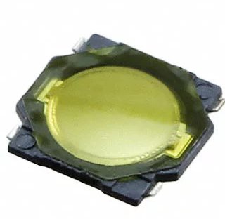
Thus, we started to search for the thinnest button we could get: standard tactile switches are too thick, and the first idea is to reduce the button shaft length, eventually remove it altogether. Performing a search on Digi-Key for tactile switches sorted by actuator height off PCB leads to these 0.35 mm height, 4.10 mm square button:
![]()
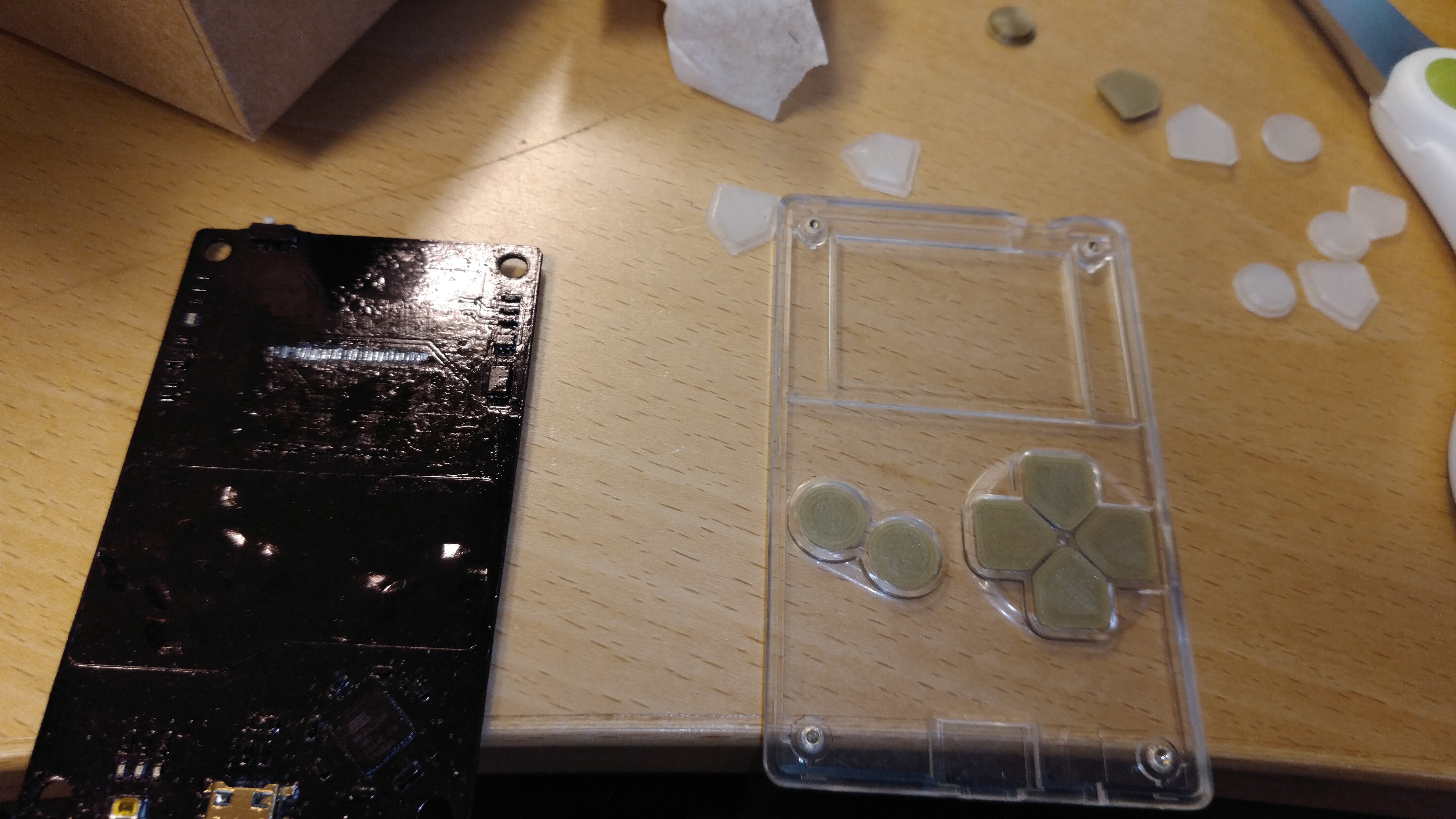
We thought we had the ultimately thinnest button on Earth, until we discovered the Arduboy tactile dome buttons:
![]()
(Check the #Printable buttons for tactile domes project for more details).
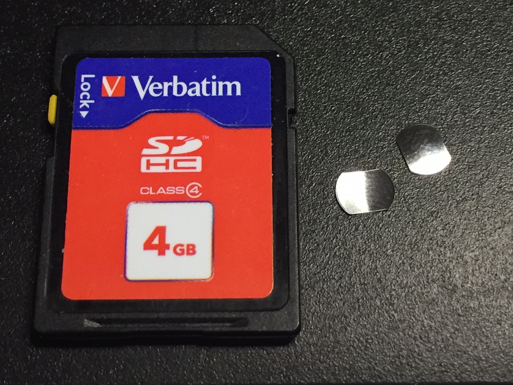
The secret is using these tiny metallic pieces that are curved (0.3 mm height for these example ones) and act as springs:
We found these RK22170 models at Snaptron, which were very kind to provide us a free sample kit and a hundred of these (easy to lose) thingies.
The only PCB footprint you need are 2 bare copper arcs with a central copper circle (no solder mask on all of these!), the dome will make an electric contact between these when pressed. You also need a small ex-centered vent hole to help the air below the button to escape on the bottom side of the PCB, that's all!
In order to keep them in place, you need to stick the domes on a piece of rubber tape, and it is actually not that easy: the required accuracy is rather tight, as the upper plastic button must press right in the middle of the dome, or the button stroke is extremely shorten.
Although we did the PCB with these footprints, we are not sure yet if we will keep these or not, or go back to our previous SMT ones because of this strict alignment problem: SMT assembly seems much easier to perform than glue these jumping domes on a piece of rubber tape.
Rear LEFT/RIGHT and RESET Buttons
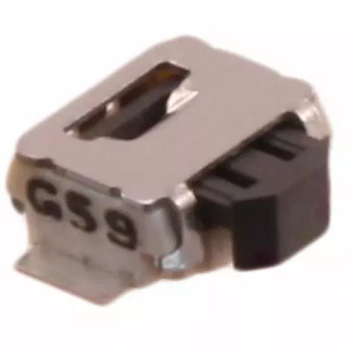
For these buttons, we needed the smallest right-angle SMT buttons possible, and we found these B3U-3000P(M)-B models from Omron (3 mm x 2.5 mm x 1.2 mm, without shaft) :
![]()
We choose the model with a boss and made a footprint with a hole in the PCB in order to have a mechanical pin that would make this SMT button resist large forces that could tear it off the PCB.
For the RESET button, it is mounted recessed on the PCB and will require a small paper clip to be inserted in a hole on the enclosure to activate it.
As for the rear LEFT and RIGHT buttons, we designed a 3D printed piece with a flexible axis between the 2 large external plastic buttons that presses on the actual button shaft with some very nice elasticity. We were a little bit skeptical about this solution when we designed it, but it proves to be quite nice, the haptic characteristics are very good!
ON/OFF Slider
We wanted to have a real ON/OFF slider, but as usual, we needed it to be as small as possible!
However, as this is a power switch, it had to withstand the maximum current that the device could draw, ~200 mA.
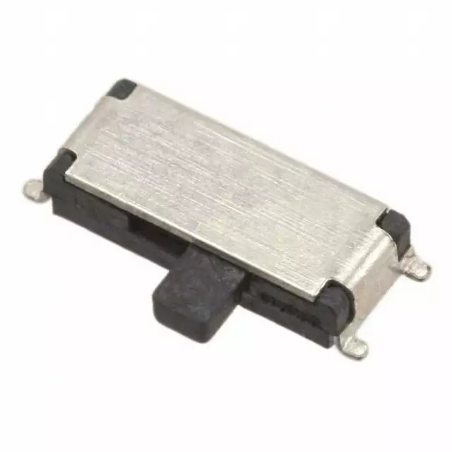
We found this small PCM12SMTR slider switch that can handle 300 mA which is only 6.7 mm x 2.6 mm x 1.4 mm, without the knob:
![]()
ESD Protections
As discussed in our previous log, it is very important to protect all user-accessible buttons and keys from ESD by adding a TVS diode as close as possible to the button pins, with a short path to a good ground plane in order to shunt the ESD energy to ground as much as possible, thus protected all subsequent devices connected to the button.
For this purpose, we used some tiny 0402 bidirectional TVS diodes mounted as close as possible to the buttons (oops, well, we did not put one on the ON/OFF slider switch, just forgot it!).
Pull-up Resistors
We also provisioned a 0603 resistor footprint near all the U/L/D/R, A/B/X/Y, rear LEFT/RIGHT and START/SELECT buttons to mount pull-up resistors. This should not be necessary as the Allwinner V3s already has internal pull-up resistors, but this may be nice to have in case e cannot active them for some reason in the Linux Device Tree description.
-
Design Decisions: The Screen
05/13/2018 at 17:46 • 0 commentsApart from the core itself, the next important decision is the the choice for the LCD screen.
Dimensions
As stated earlier when we discussed about the core, the whole point for the FunKey Zero project was to prototype as much features as possible for the #Keymu - open source keychain-sized gaming console device.
We determined that the maximum dimensions should not exceed ~ 40 mm x 40 mm x 15 mm, or we should not call it a keychain emulator anymore ;-)
For the Keymu, we considered that the screen should be as large as possible and adopted a "clam shell" form factor to protect the fragile screen and buttons from impacts on the keychain.
But these decisions seriously restrict the available screen size: if you consider that the screen can fill the whole 40 mm x 40 mm surface, the maximum possible standard screen size that works is then 1.5" or 38.1 mm in diagonal, or 26.94 mm square.
Screen Interface
First of all, the picture to be displayed must be buffered ("frame buffer") on one side, either on the CPU side, or in the screen module itself, which leads to 2 different screen module types:
- in the first case, the screen module does not contain any RAM and is just a "dumb" display that needs to be constantly refreshed in order to display a picture, using pixel clock, horizontal and vertical sync signals, and of course, the pixel data, usually in an RGB666 (18 data bits from D0 to D17) or RGB888 (24 data bits from D0 to D23), plus a few additional signals. These screens are mostly used to display "live video" coming from a camera sensor like in Handycams or dashboard cams
- in the second case, the screen module contains a memory, often called Graphic RAM (GRAM) that does not need constant refreshing in order to display a picture. This type of screen is generally used for static displays like UI with buttons, check boxes and sliders
In the case of "dumb" screen module, the screen interface is generally called "RGB", with a variant "RGB8" where each color component is transferred one after the other (each pixel needs 3 transfers).
For the screen module featuring internal GRAM on the other hand, there are several standard interfaces used to drive them:
- for the smallest screens, an I2C bus is used. As these screen do not contain many pixels, the I2C bus with its maximum speed of 400 Kb/s is more than enough to drive these, and it only requires 4 wires: VCC, GND, SDA (Serial DAta) and SCL (Serial CLock). At 25 fps and 65536 colors, the maximum resolution you can expect is thus... 32 x 32 pixels!
- for screens with more pixels, the I2C bus just is too slow to allow high fps numbers, and an SPI bus is used instead, which requires a few additional wires, usually: VCC, GND, SDI (Serial Data In or MOSI), SCLK (Serial CLocK), CS (Chip Select), RS (Register Select), RESET and most of the time a separate power supply for the LED backlight. Speed is often specified up to 8 or 10 MHz, and at 25 fps and 65536 colors, the maximum expected resolution is 128 x 128 pixels. But it is not uncommon to have integrated screen controllers going up to 40 or 50 MHz and in this case, the resolution can go up to 240 x 240 pixels with the same picture parameters!
- in order to reduce the required interface speed, some screen modules use parallel buses with 8, 9 , 15, 16 or 18 bit bus, dubbed "MCU", "MPU", "Intel", "8080" or "6800"
- for the screens with the highest resolutions (including the ones used in smartphones and tablets), the interface used is a high speed differential serial, user-unfriendly interface called MIPI DSI (Display Serial Interface) requiring a specific controller, only available in high-end mobile phone CPUs
Clearly in our case, solution #1 is not possible, as well as solution #4, as we don't have the corresponding DSI interface in our CPU. This leaves us with solution #2 or #3 or a dumb screen with RGB or RGB8 interface.
Hinge
Because of the constrained dimensions, we want to use a "clam-shell" design, like the cell phones from some years ago. This implies a hinge between the screen and the main enclosure body, into which the screen module flat cable must go into.
But in order to remove some mechanical stress from this flat cable, the flat cable should not go straight through the hinge or chances are that it will break very quickly after several lid open/close sessions.
The solution is to roll the screen flat cable into the hinge internal cavity much like a sticky fly ribbon.
This means that the screen module flat cable should be as long and as narrow as possible, which is only possible for solution #2 above, i.e. using an SPI bus.
Screen Resolution
Given the constraint of a 1.5" screen size and an SPI interface with a long flat cable, a quick search on AliExpress / AliBaba provides a long list of similar screens, which resolution does not exceed 128 x 128 pixels: we used one of these in our Edison-based Keymu device.
But based on our previous experience, we knew that this resolution is not sufficient to play retro games featuring small fonts, even when using anti-aliasing.
So we kept searching and we got excited several times when finding 1.5" screens with a 320 x 320 pixel resolution, but every one of them turned to use an impossible MIPI CSI interface :-(
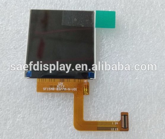
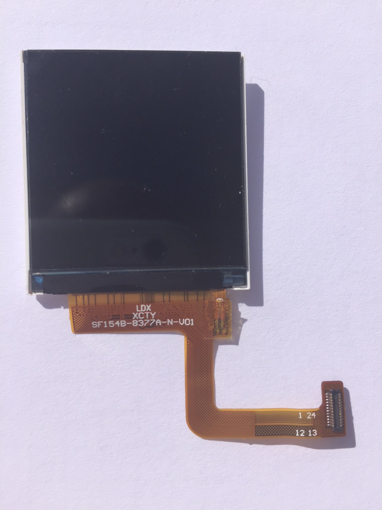
This was until we found this 1.5" screen using an SPI interface and with a 240 x 240 pixel resolution:
![]()
OK, well, the ribbon cable may not be long enough to be rolled into the hinge... But this is something the manufacturer can customize for a fixed tooling fee of $800...
And despite what is specified in its ST7789V controller chip datasheet, its SPI write clock cycle can be much shorter than Twc= 66 ns (15.15 MHz) and can go actually up to ~60 MHz!
We asked the manufacturer about this performance and they confirmed the achievable speed, as well as the ability to use a +3.3V voltage for the backlight LEDs instead of the specified +2.9V. BTW, this is another positive point for this screen: the backlight LEDs are wired in parallel and not in series. This raises the current requirement, but also lower the LEDA/LEDK voltage and removes the need for an additional step-up voltage converter just for this purpose.
And now the cherry on the cake: this screen has both a wide angle of vision of 80° and a contrast of 400:1 thanks to its IPS technology!
Last but not least, the ST7789V is also readily supported in the stock Linux kernel fbtft driver to provide a frame buffer over the SPI bus.
A breakout board for an equivalent screen (not same pinout and connector) featuring the same ST7789V controller chip is available at Adafruit.
-
EMC: EMI, RFI, ESD
05/12/2018 at 08:50 • 0 commentsNo, these acronyms are not new state-sponsored 3-letter agencies, but they are sometimes considered as dreadful!
ElectroMagnetic Compatibility: ElectroMagnetic Interference, Radio-Freqency Interference and ElectroStatic Discharge, this is what these mean.
This subject is seldom covered during hobby electronic discussions, because it is not essential (things will "work" without them), it is difficult to understand and in this regard is like some kind of "black magic", and even if you already know it, this subject is just boresome;-)
So why bother?
Actually, our own experience shows us that EMC is really the difference between a working prototype on the bench and a reliable product in the wild!
Another serious motivation is that any device must be certified for compliance against EMC standards in order to be transported, sold, distributed or even used outside a lab.
This is why we decided to take EMC into consideration right from the start for our FunKey Zero project, as the goal is to prototype as many features as possible for the #Keymu - open source keychain-sized gaming console that we would really like to turn into a usable end-user product.
EMC
ElectroMagnetic Compatibility (EMC) is both a device characteristic and a branch of electrical engineering that deals with unintentional generation, propagation and reception of electromagnetic energy which may cause unwanted effects. The corresponding issues are emission (whether deliberate or accidental), coupling and susceptibility (or its opposite immunity).
Please note that from an EMC compliance test point of view, this means that a device is potentially both a source and a victim of interference.
EMI
On the other hand, ElectroMagnetic Interference (EMI) is the disturbance generated by an external source that affects an electrical circuit, i.e. it is the phenomenon itself, not the characteristic or the study of it.
As the equivalent electrical element between 2 coupled devices is a complex impedance that can be a resistor (R), a capacitor (C) or an inductor (L), or any combination thereof, the coupling can be linearly detailed as conduction, electrostatic coupling or electromagnetic induction, respectively.
Continuous Interference
A Continuous Wave (CW) interference arises where the source continuously emits in a given range of frequencies. This type of interference is divided into sub-categories according to the considered frequency range.
For lower frequencies (typically less than a wavelength), conduction coupling is predominant and may affect 2 conductors in phase (such as a disturbance that hits both conductors at the same time) or out of phase. In the first case, this phenomenon is called common-mode coupling, whereas the second is called differential-mode coupling. This distinction is important, as the first class of common-mode coupling may be more easily handled to greatly attenuate the disturbance when the 2 conductors carry opposite signals ("differential signals"), whereas the second class of differential-mode coupling is much more difficult to deal with. In this last case, only frequency filtering is effective.
RFI
For higher frequencies and when the source and victim are separated by a large distance (typically more than a wavelength), both devices act as radio antennas: the source emits or radiates an electromagnetic wave which propagates across the space in between and is picked up or received by the victim. In this case, coupling is then achieved by radiation.
Radio-Frequency Interference (RFI) is thus a special case of EMI, for which disturbance are electromagnetic waves whose frequencies lie in the range extending from around 20 kHz to 300 GHz (the upper limit constantly increases as technology pushes it higher!), roughly the frequencies used in radio communication.
Pulse or Transient Interference
An ElectroMagnetic Pulse (EMP) arises when the source emits a short-duration pulse of electromagnetic energy. This event may be repetitive, such as for artificial sources like electric motors, electric ignition systems or continuous switching digital electronic circuits like DC/DC voltage converters.
Sources of isolated or short series of EMP are: power line surges / pulses, Lightning ElectroMagnetic Pulses (LEMP) and Nuclear ElectroMagnetic Pulses (NEMP).
ESD
ElectroStatic Discharge (ESD) arises when differently-charged objects are are brought into direct contact or close together and when the dielectric between then breaks down, often creating a visible spark in the air. In this regard, ESD is a special case of EMP.
ESD voltage on any device creates a large surge current which will flow through ohmic drops and if these resistances are large enough then it will create huge internal voltages.
Inside semiconductor ICs in particular, this may lead to catastrophic damages like direct punch holes in the substrate, or any other more subtle damages due to Electric Over-Stress (EOS), i.e. whenever the component operates beyond its absolute maximum ratings.
In order to test the effectiveness and reliability of ESD protection circuitry, the JEDEC industry standards for ICs are defining several test models (sources: http://www.electronicdesign.com/power/what-s-difference-between-hbm-cdm-and-mm-test and http://www.vlsifacts.com/esd-models-and-their-comparison-esd-part-2/):
- Human Body Model (HBM). This model represents an ESD event between a human body and an electronic component. HBM model helps to simulate stress level developed by electronic component through human touch discharging the static charge through device to ground. Its model and pulse waveform are:
![]()
Machine Model (MM). This model represents an event when a machine or an automatic handling unit touches the IC. This is highly likely when there is a metal to metal contact during production. Machine model is not used very often nowadays since fabrication is all automated and ESD-free. Its model and pulse waveform are:
![]()
Charged Device Model (CDM). This model assumes the IC itself is charged and then touches any ground plane. The CDM also addresses the possibility of charge residing in the package and later discharge through a pin which is grounded. Its model and pulse waveform are:
![]()
A combined pulse waveform superimposition of all the above models gives:
![]()
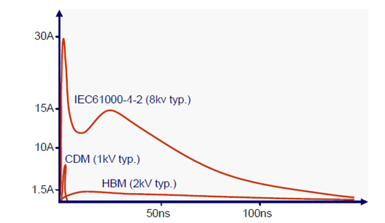
In addition, at the system (device) level, the IEC defines a System Level Model in IEC 61000-4-2 test, which has typically 8 times higher testing voltage than CDM, and 20 times higher peak current testing than HBM. This is a model which assumes the electronic components to be mounted on the PCB and requires the system to be powered up and operating. This is similar to the previous component level models but at much higher stress levels. The typical requirement is 4KV – 8KV (ouch!):
![]()
Now What?
Now that we know our enemies, what should we do to protect our device and make it compliant to regulations so we don't disturb other ones?
Let's review all the measures we can take!
Shield
If possible, we should put a metallic shield around the electronic circuit. This is not very convenient for prototyping, but it helps a lot both to protect against external EMI and to avoid leaking EMI.
If the shield is solid metal, and all the shielded connectors are bonded to it (with EMI fingers). All noise is shunted around this path, all noise currents due to self-capacitance, due to current riding along to other cables, whatever. Everything inside is oblivious to all this happening, because it's a Faraday cage. The continuous, low impedance shield is an absolute requirement to achieve this.
Actually, a shield may be required by some regulations, like does the FCC Part 15.247 for RF electronic circuits.
Enclosure
If a metallic shield is not possible, at least the electronic device must be contained within an enclosure to protect it from direct contact ESD on most of its surface.
On one hand, it completely spoils this very nice tech-look, but on the other hand, it may save your day when you spill a beverage on it!
And you can always use a transparent casing;-)
Ground Plane
If you don't have a metallic enclosure, you're a bit more pressed for options. A circuit board with solid ground plane is as good a substitute as you can get.
Having a solid ground plane helps a lot to reduce EMI emissions by reducing the distance between a possible perturbing signal and the ground. Having a continuous ground plane also helps to evacuate incoming EMI energy and avoid sensitive electronic chips.
Grounding
Collecting EMI energy with a continuous ground plane is one thing, but this energy must be evacuated, and a proper grounding is the only solution. However, this is not always possible, like for a portable device, for example.
ESD Protection
ESD may have very nasty effects on semiconductors, and even when protected by a shield or a simple non-metallic enclosure, they may still hit the electronic device by contact or close proximity through ALL externally accessible devices: buttons, sliders, connectors, jacks, LEDs, LCD displays, loudspeaker, antennas...
In order to prevent ESD, EACH SINGLE supply or signal trace connecting this device on the PCB must feature a Transient Voltage Suppressor (TVS) device, placed as close as possible to the externally accessible component pin and connected to a good ground plane:
![]()
If we try to avoid Quantum Physics altogether, it is sufficient to say that these TVS devices are a kind of avalanche diodes, that are like a small capacitance (a few pF) when a voltage lower than a given threshold is applied between its pins, and convert into a short when the voltage is higher.
The main characteristics of these TVS diodes are their capacitance value, threshold voltage, maximum allowed pulse voltage and duration, trigger time, and if they allow monodirectional or bidirectional current flow through them (used when a signal may be negative relative to ground).
EMI Filtering
Event when using a metallic shield to avoid radiation, EMI can still find its way in/out by conduction through all connected wires: power supply cables when applicable, and through all data cables and connectors.
For the general differential-mode coupling case, the solution is to add electronic filters that will remove all unwanted noise outside the expected frequency range. They may be band-pass or low-pass filters, and you can find some integrated filters (eventually with combined ESD protection) to add to your circuit, Ferrite bead choke to clamp onto a cable, or you can make your own filter using discrete components.
The connections that requires such EMI filtering are : audio jacks, USB power, externally accessible UARTs and all otherwise accessible data lines.
Common-Mode Noise Suppression
As explained above, common-mode interference is when a disturbing source pollutes 2 conductors with the same perturbation. In the case where the 2 conductors carry 2 differential signals that are always opposite, the perturbation can be removed almost completely using "common-mode choke".
This is very effective for Ethernet, for example, which specifications require transformer coupling, usually with some common mode filtering to take the edge off, and a 1nF capacitor, from center tap to ground, to handle ESD. It is usually combined with Bob-Smith termination resistors for the cable side, and 50 ohm termination resistor for the PHY device side.
Unfortunately, this is not true for USB which has poor common mode rejection, even in true differential High Speed mode, and no, common-mode filtering won't help here -- the USB signaling method with pull-up / pull-down resistors is not designed to accommodate that, unfortunately).
USB Device Shield / Ground Connection
Warning: this is a highly controversial subject and may trigger a flame war!
If the above EMI recommendations are mostly accepted, including for Ethernet connection (well, except maybe for the USB common-mode...), it seems that for this subject, contradictory recommendations abound, each with its own unsupported claims. Even authoritative-sounding sources such as Intel, Texas Instruments, FTDI, Cypress Semiconductor and Atmel / Microchip seem to disagree on the correct way to handle the cable shield on USB devices:
- The Hardware Book website recommends not to connect the cable shield to ground on the device at all
- Intel (Section 5.4, p. 9) recommends to connect the shield directly to signal ground
- TI (Section 2.2.4, p.3) recommends to connect the shield to signal ground through a ferrite bead
- FTDI (Section 3.2, p. 11) recommends to connect the shield to signal ground through a capacitor
- Cypress (Figure 7, p. 7) and Atmel, now Microchip (Section 3.3.3, p. 8) recommend a 1 Mohm resistor in parallel with a 4.7 nF capacitor
The only reason to follow opinion #1 would be to avoid ground loops by connecting the shield on both side to grounds at different levels, but because USB cables are so short, ground loops aren't really much of an issue.
Opinion #2 will actually work, even when exposed to EMI (and won't radiate itself). The downside is, all that EMI is conducted over your board's ground, and will find its way out any cables attached to it.
In Opinion #3, the ferrite bead blocks the EMI RF noise but does pass DC allowing DC level between systems to be aligned. The problem is that this system does not deal with ESD, which has no path to ground. I have seen such 0603 ferrite beads melted by a distant lightning strike!
As for Opinion #4, if using a high voltage capacitor (> 500V), this may effectively shunt the EMI RF noise and ESD to ground, but it does not pass DC allowing DC level between systems to be aligned. It is not a problem though if the device is portable and not connected to any other ground.
Opinion #5 is the ultimate one, the resistor creates equipotential between system ground and chassis ground, and the (high-voltage) capacitor shunts the EMI RF noise and ESD to ground.
Conclusion
EMC issues are often underestimated and not well understood. It is however important to take them into consideration during the design phase, should the device be sold one day or the other.
If EMC is not required during the prototyping phase of a device on a workbench, compliance against EMC rules and standards is absolutely mandatory to be able to distribute it as an end-user product.
The few design rules above should be enough to cover most simple cases, and use as guidelines for more complex ones.
- Human Body Model (HBM). This model represents an ESD event between a human body and an electronic component. HBM model helps to simulate stress level developed by electronic component through human touch discharging the static charge through device to ground. Its model and pulse waveform are:
-
Design Decisions: The Core
05/09/2018 at 11:56 • 3 commentsForm Factor
The main goal for the FunKey Zero project is to prototype the maximum number of features for our final #Keymu - open source keychain-sized gaming console machine. The keychain form factor is the most limiting parameter: roughly, we determined that 4 cm x 4 cm x 1.5 cm were the maximum allowed dimensions to stay practical, which leaves just enough room to fit a 1.5" screen, not much larger. This rules out event the small Raspberry Pi Compute module (67.6 mm x 30 mm) or Zero (65 mm x 30 mm) as the core processor board for the project.
Screen Resolution
With a lot of tricks, it is possible to stuff some emulators with a 128 x 128 pixel resolution on an ESP32, for example, like the small PocketSprite.
But based on our Edison Keymu experience, we determined that a 128 x 128 pixel resolution was barely acceptable to play some games with small fonts, so we tried to get a screen with a higher resolution, still fitting the 1.5" size.
If you search well, you can find on AliBaba some screen in this form factor with a resolution of 320 x 320 pixels but unfortunately, to handle the large amount of data to display, they use a high speed differential serial, user-unfriendly interface called MIPI DSI (Display Serial Interface) requiring a specific controller, only available in high-end mobile phone CPUs :-(.
We were lucky to find a nifty 240 x 240 pixel 1.5" screen with a simple SPI interface that is just perfect, which is now available at Adafruit.
RAM
However, a 240 x 240 pixel in 24-bit RGB color image takes a little bit more than 168 KB of RAM memory to store in a frame buffer, which is out of reach for most Micro-Controller Units (MCUs), except for the largest one.
Instead, we turned to bigger Central Processing Units (CPUs) with enough RAM memory, and if possible able to run a Linux OS in order to benefit from the existing software base, including already running game emulators.
But this extra RAM comes at a price: to reach these capacities, you need to use Dynamic RAM (DRAM) instead of the Static RAM (SRAM) used in MCUs. These are generally provided as external chips, with high-speed bus connections, requiring extra-careful PCB layout and trace routing, not counting for the required real estate on the board.
CPU with Integrated DRAM Memory
Considering the Raspberry Pi, for most models, this DRAM complexity problem was solved using a clever technique called Package on Package (PoP), which consists in soldering the DRAM package on top of the CPU itself.
Unfortunately, only a few chips outside the unreachable Broadcom CPUs used in the Raspberry Pi are using the same technique :-(
We found Next Thing Co.'s GR8 chip which combines a 1GHz Allwinner R8 ARMv7 Cortex-A8 processor with NEON SIMD extensions and a Mali-400 GPU. 256MB of DDR3 SDRAM in a single 14 mm x 14 mm x 0.8 mm package. Hopefully, we only found it too late, as Next Thing Co. is now dead, RIP.
Another option is the Octavo OSD335x-SM module which combines a 1GHz TI Sitara ARM Cortex-A8 AM335x processor and up to 1GB DDR3 memory into a slightly larger 21 mm x 21 mm x 3.08 mm package. This chip is used in the PocketBeagle. Sure, it contains almost all the required components, but it is about 1/4 of our total PCB area... More worrisome, this chip (like the GR8) is based on an older design ARM Cortex-A8, which has been superseded by the smaller, simpler and more power-efficient ARM Cortex-A7 in 2013. Be careful, the ARM version numbering is very confusing!
We then discovered the Allwinner V3s chip wich combines a 1.2GHz ARM Cortex-A7 with NEON SIMD and VFPv4 extensions and 64MB DDR2 memory into a user-friendly 16 mm x 16 mm x 1.6 mm (including pins) LQFP128 package. No more worries regarding the power consumption, but now some concern about the small DRAM memory size... (Note: in the meantime, Allwinner introduced the V3, which is the same CPU with 2x or 4x the amount of DRAM in a smaller 12 mm x 12 mm TFBGA package!).
Evaluation Board
In order to quickly evaluate the V3s performance in terms of power consumption and DRAM memory size, we wanted to get a ready-made evaluation board.
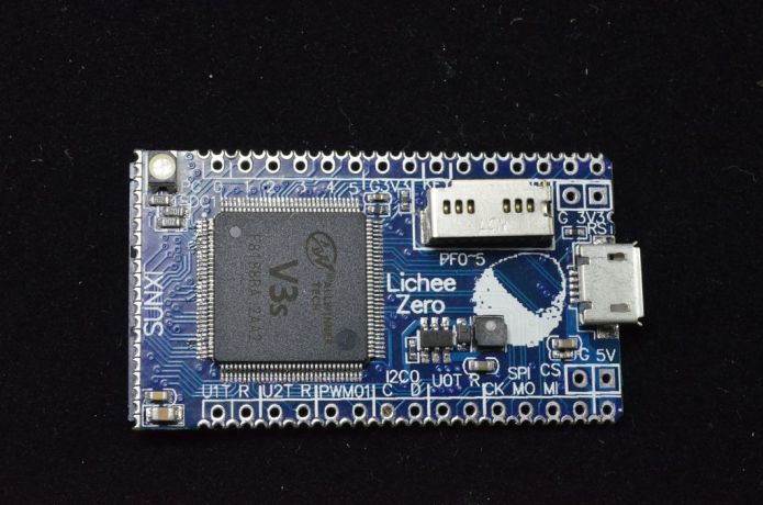
The only one we could find was the LicheePi Zero. We missed the Indigogo campaign by a few weeks, but we eventually got some boards in August 2017. Today, they are very difficult to get, the only place you can find them is on TaoBao for ¥47 (USD 7.40), you need to select "zero核心板" ("Zero Core board"). But ordering on TaoBao is quite an experience, good luck!
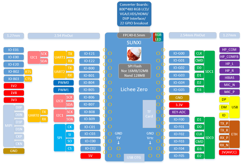
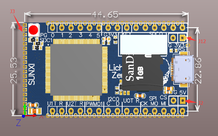
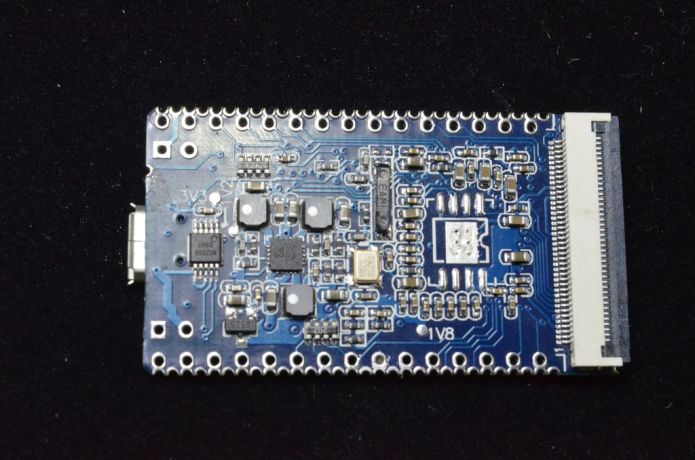
This board features the AllWinner V3s chip we need and exposes most pins on a convenient dual pitch (1.27 mm and 2.54 mm) rows of holes on the board edges, so that you can both mount through-hole headers to use on a breadboard, or solder it on a main PCB as an SMT module.
The LicheePi Zero module can be powered either from its built-in Micro-USB OTG connector, or using its +5V pin. We do not want to use the micro-USB, as we want to be able to insert an automatic switch known as an "ideal diode" to disconnect the +3.7V LiPo battery when operating from the USB +5V power supply, and there is no way to do this on the board. Hopefully, the USB data signals USB_DP and USB_DN are both routed to the board edge pins, so we can use an external micro USB connector:
![]()
It is not documented in this pinout, but there is indeed a RESET castellated pin on the right side of the USB OTG connector.
The LicheePi Zero module contains an SD/TF Card holder (simple one, no push-pull type), and the only modification we had to perform was to desolder the 3 resistors near the RGB LED at the top right corner of the board, as they interfere with some of our GPIO usage. We do not use at all the top FPC40 connector.
As you can see, almost all V3s pins are broken out to module pads, either on a 2.54 mm or 1.27 mm pitch.
Controlling on the V3s datasheet, this module almost perfectly matches our needs:
- 12x GPIOs with interrupt capabilities for the buttons (U/D/L/R and A/B/X/Y pads, rear L & R buttons, plus START and SELECT buttons)
- 1x Analog audio output to play on a speaker (using an external audio amplifier chip) or on headphones using an audio jack
- 1x RESET button
- 1x USB device interface to mount as a memory device on a host
- 1x UART for console debug
- and of course, 1x SPI bus plus some extra GPIOs (LCD_RESET, RS and PWM for screen backlight) for the LCD screen!
There is even a spare I2C bus that can be convenient to control some external Power Management IC (PMIC) in our #Keymu - open source keychain-sized gaming console!
The LicheePi Zero module form factor is a little bit too large for our #Keymu - open source keychain-sized gaming console, but still very close:
![]()
In the #Funkey Zero, we turn the module 90° CW and used it as an SMT module, which requires a "U" slot on the main PCB as the LicheePi zero features components on both sides of the PCB. Given the central LCD position with keypads on both sides, this almost fixed the overall shape and dimensions of the design.
-
Licenses & repositories
04/23/2018 at 08:40 • 0 commentsThe software released for the FunKey Zero project is licensed under the Gnu General Public License, version 2 or (at your option) any later option.
This includes the material provided in our buildroot-licheepi-zero Github repository.
The electronic hardware and mechanical design are released under the Attribution-ShareAlike 4.0 International (CC BY-SA 4.0) license.
-
Current state of things
04/22/2018 at 14:50 • 2 commentsHi everyone, many logs/files/links have been published in the last couple of days ! We’re very excited to be sharing all of this with you but we know it’s a lot of information, so if you are a bit lost and wondering the exact state of advancement of Funkey Zero this log is for you.
Mechanical design and printing
The mechanical design is done and tested. If you remember that Keymu was made with Solidworks, this time, we redesigned everything from stratch using Fusion 360. You can find the source files in the project links or here.
We printed and tested the tolerances of our design using a Prusa i3 MK2 with a 0.1mm precision and a classic nozzle width of 0.4mm. Appart form the buttons which are still a bit too large, your prints should all fit together pretty easily. One precision though: we printed the top part in 2 halves, as well as the bottom part. See this log for more precisions. It is up to you to follow this method or not obviously but, believe us, it leads to pretty nice results.
Electronics and Assembly
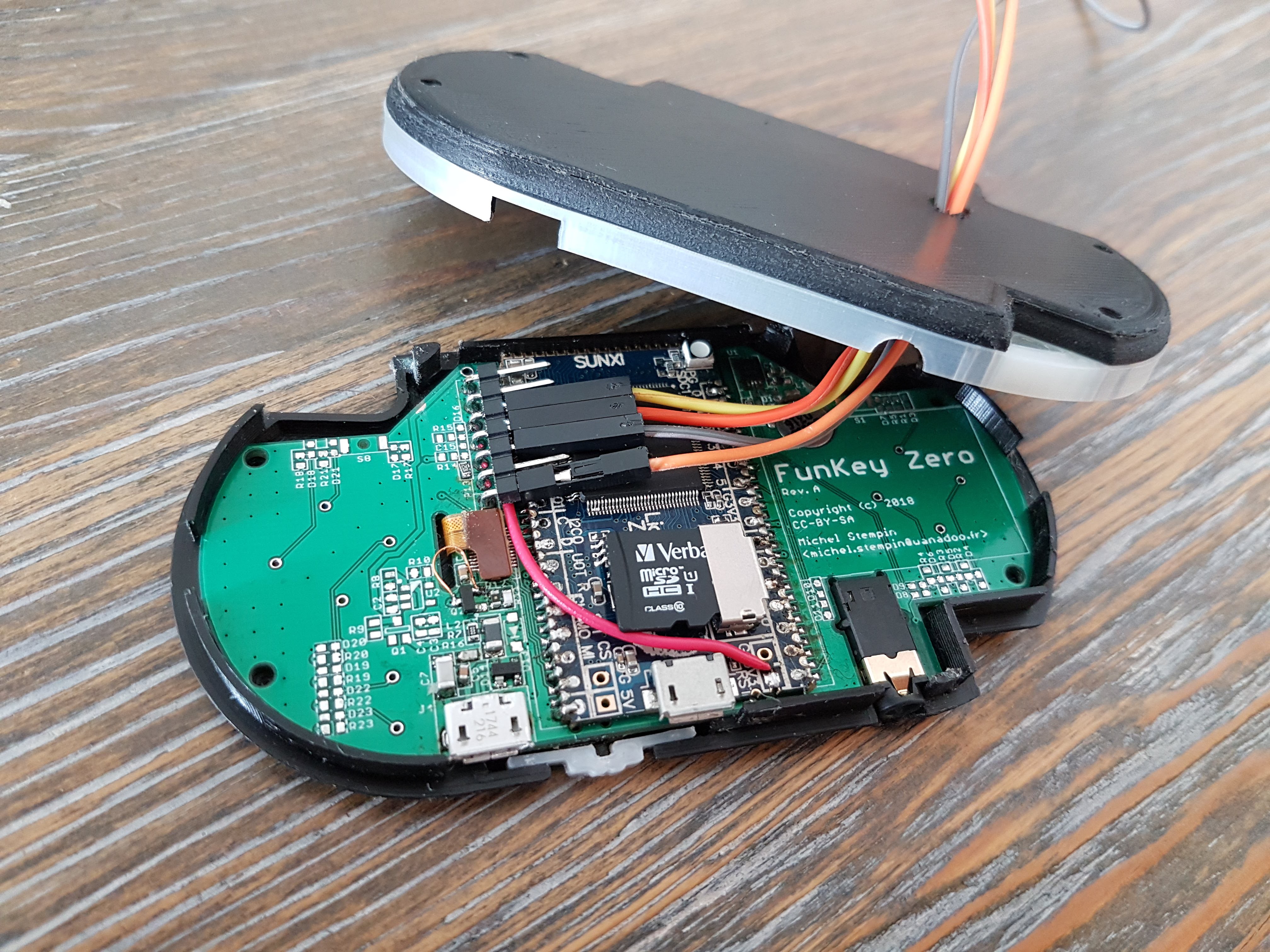
Right now we have soldiered the essential parts : power management, screen, audio and debug pins. We have cut a hole in the bottom half of the case on order to let debug serial cables get in as you can see in this picture :
![]()
The PCB/Case assembly went great: for now there are no problems of tolerances, but we still have not put the snap domes and tested the buttons, so we’ll keep you updated.
Regarding what’s been soldiered we had some minor issues for the screen and had to add a few cables, the power management part and the audio Jack work perfectly but not the speaker for now. It might be the soldiering itself or something else, we’ll have to dig a bit deeper but it should not be a serious issue.
The BOM and schematics have been shared with you obviously, so if you want to join us in this debugging fun we’ll be more than happy to welcome you 😊
Software side
On the sofware side of things, things are going pretty smoothly for now but we still have a lot of work.
Boot time and Logo
As you might know from our log "Linux Distribution", we developed our own linux distribution from the ground up for Funkey Zero and we are very proud to say that the boot time in under 3 seconds. It’s so fast we made a video for you to be able to believe us :
As you can see we also added a boot logo, which is – for now – very simple and prone to evolve. But it’s still nice to be welcome by something else than a serial console.
Usb mass storage
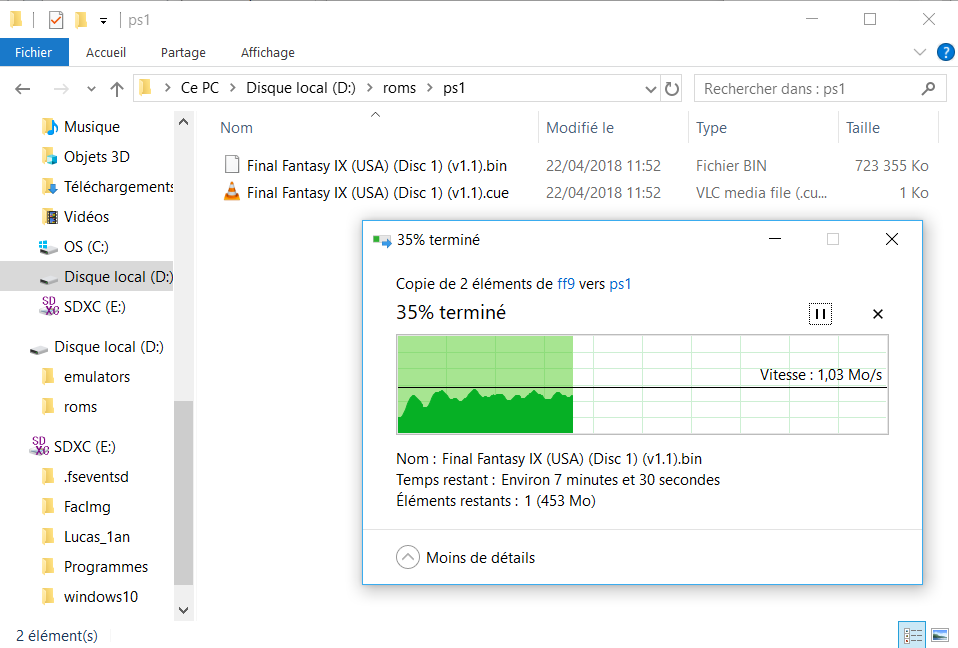
Part of our new distribution is the possibility to connect Funkey Zero to any computer and it will be mounted as a USB mass storage device… basically a usb key. There is no easier way to transfer your roms than this :
![]()
Optimized Emulators :
Guys, having a 240x240 screen resolution is great. On Keymu the resolution was 128x128 and was acceptable but not very comfortable to play games such as Zelda or Pokemon in which you need to read a lot. This time, with Funkey Zero, the resolution is very comfortable, so even if our processor only has 64MB of RAM and a single core 1.2Ghz processor, we wanted to be able to make the most of it.
Thanks to optimized emulators for ARM made mostly by notaz for the Pandora, we were able to re-adapt and re-build many emulators for our ARM v7 processor and our 240x240 resolution. We realized that once optimized, the V3S processor was actually a surprising powerhorse ! It even runs PS1 games at only 70% CPU load. And guys, oh what a pleasure to hear and see Final Fantasy IX running on this thing !!! Words are not enough, just watch :
For the future, we plan to port many more emulators and the work is in fact already underway so stay tuned 😉
TODO
So… if in the video above you didnt see me playing it’s for a reason : the buttons and the whole button mapping interface is still under development. It is in fact quite a lot of work to map GPIOs to keyboard letters. We had to recompile the Kernel to add the uiput module and basically pretty much recode our own version of Pikeyd (a library for raspberry dedicated tot his issue) in order to adapt it to the V3S and to our customized OS. The work is almost finished so you should see a video of us playing pretty soon.
The only unknown yet is the frontend app we will use. Most of them, like Emulation Station, require MESA, which is very heavy and risk to overweight our lightweight custom distribution for a few animations… So we’re still looking into it 😉
Anyway thanks to you all for your interest in Funkey Zero and we promisse a lot of news very soon, so stay tuned !
-
Linux Distribution
04/21/2018 at 20:29 • 3 commentsDistro Choices
The AllWinner V3s and by extension the LicheePi Zero are designed to run Linux kernel-based operating systems, which includes both a distribution called "CamDroid" (a lightweight operating system based on Android) with a good support for MIPI cameras and H.264 video codecs, or more conventional Linux-based distributions, with a choice between an EmDebian or buildroot-based distribution.
Camdroid
We definitely discarded the CamDroid distro, as it requires the non-public AllWinner SDK to build which is encumbered with closed-source blobs, as we don't need its specificities here. Moreover, support seems very difficult, as all that can be found is mainly in Chinese.
Regarding plain Linux distros, there are some pre-built EmDebian and buildroot-based images with several build options (Xorg, gcc, Python, LXDE, minimal) available for download at https://licheepizero.us/.
EmDebian
Despite its attractive Debian-flavored facilities (well-known structure, number of available pre-built binary packages), we also discarded the EmDebian distro because:
- This distro is dead: "As of July 2014, updates to the Emdebian distributions ceased. There will be no further updates and no further stable releases."
- Even if it is tagged as "embedded", the resulting size is rather large for such a small amount of RAM
- boot time is > 10 s
Buildroot
Thus, we turned to buildroot to provide our distro. "Buildroot is a simple, efficient and easy-to-use tool to generate embedded Linux systems through cross-compilation.". And this is really true:
- its core infrastructure is just a few hundred lines of make code
- it uses make code and kconfig for the configuration interface and language. Both technologies should be familiar to all embedded Linux developers
- compiling the whole distro is fast and don't take hours, even when re-building the cross-toolchain from scratch
- it is designed for small to medium sized embedded systems
On the down side, there is no runtime package management system (dpkg, rpm) and complete rebuilds are often required...
Linux Distro Dissection
Actually, an embedded Linux distribution is not a single piece of firmware: a first consideration are the required tools that are running on the host or build system, as opposed to the software running on the target machine.
Host
In the case of buildroot, you have the core system which is made up of a few hundred lines of make code and kconfig scripts to run a simple menuconfig-like configuration interface. There are also a few required utilities that are built from their source tarball packages. But the piece of meat is the cross-toolchain that includes all the tools required to build executable software that will run on the target machine. With buildroot, you have the choice either to use a pre-built toolchain or build your own from scratch. Guess what we chose ;-)
Target
On the target side, each independent piece of software is called a package, and is made up of a small, mostly declarative makefile, some patches and the source tarball package that is fetch from the original package maintainer location. These packages are cross-compiled using tha above toolchain and put into a set of firmware images that are burned into the target machine.
Even on the target machine, there are several distinct pieces of software that must be considered, described here in their boot order:
Boot ROM (BROM)
This one cannot be modified, as it is a read-only software that is first run upon boot-time. It is in charge of bringing up the minimum resources to startup the CPU. It also reads some GPIO inputs with either pull-up or pull-down resistors known as bootstrap configuration to select some operating options such as clock frequency, boot device, etc.
Secondary Program Loader (SPL)
The BROM then fetches the Secondary Program Loader (SPL) from the selected boot device (in our case, the SD Card) into the built-in small SRAM. The SPL's main task is to initialize the DRAM in order to fetch the next boot stage from SD Card into it.
U-Boot (u-boot.bin) and boot.scr
The SPL then loads the main U-Boot bootloader into the main DRAM and executes it. U-Boot i almost an operating system by itself, as it initializes many resources and is able to run scripts (boot.scr). The goal for the U-Boot is to load the binary Device Tree and the Linux kernel into DRAM and execute the kernel with the provided DTB.
In our case, the SPL and U-Boot images are combined into a single "u-boot-sunxi-with-spl.bin" image.
Device Tree Binary (DTBs: sun8i-v3s-licheepi-zero.dtb and sun8i-v3s-licheepi-zero-dock.dtb)
The binary device tree is an OS-independent structure that describes all the hardware resources. It is compiled from a corresponding Device Tree Source (DTS) file and loaded at run time by the operating system to configure its peripheral drivers according to the described hardware.
Linux Kernel (zImage)
Based on the binary device tree, the Linux kernel will initialize all the required operating subsystems, mount the root filesystem and start the first user task, then schedule all tasks in the background.
Root File System (rootfs.ext2, rootfs.ext4 and rootfs.tar)
The root file system is a disk or Flash memory partition organized as a structured file hierarchy containing directories, plain and pseudo-files that will be used during processing. The rootfs.ext2 and rootfs.ext4 are equivalent and linked symbolically, and the rotofs.tar may be used to mount the root filesystem over NFS (Network File System) instead of read locally from SD Card.
Distro Images Generation
Buildroot is able to generate all these images (u-boot-sunxi-with-spl.bin, boot.scr, sun8i-v3s-licheepi-zero.dtb and sun8i-v3s-licheepi-zero-dock.dtb, zImage, rootfs.ext2, rootfs.ext4 and rootfs.tar and build a single SD Card image that contains them all at their expected location using a single command.
Unfortunately, this was not the solution chosen by the LicheePi developers, who instead provided a set of handcrafted recipes and scripts to build the different images and the final SD Card image:
https://www.kancloud.cn/zepan/zero_tutorial/342700
https://www.kancloud.cn/zepan/zero_tutorial/342701
https://licheepizero.us/ (look for zero_imager.zip tool)
We decided to drop these weird tools and go back to a more standard all-buildroot generation, using the custom U-Boot and Linux kernel repositories containing all the required patches for the V3s and the LicheePi Zero board, based on the LicheePi Github repositories:
We generated a proper licheepi_zero buildroot default configuration for buildroot, so that you can generate all the images using a few simple commands that are standard to build all buildroot targets. A first patch has been submitted upstream to the builroot team to integrate the LicheePi Zero board into the mainstream buildroot disitrbution. Right now, a second version of the patch is under construction. Until it is integrated into buildroot, it is available in our own repository:
https://github.com/Squonk42/buildroot-licheepi-zero
Building the SD Card image containing all the required images is then just obtained using:
$ git checkout git@github.com:Squonk42/buildroot-licheepi-zero.git
$ cd buildroot-licheepi-zero
$ make licheepi_zero_defconfig
$ make menuconfig (optional)
$ make
The resulting images are then located in the "output/images" directory:
output/images/
├── boot.scr
├── boot.vfat
├── rootfs.ext2
├── rootfs.ext4 -> rootfs.ext2
├── rootfs.tar
├── sdcard.img
├── sun8i-v3s-licheepi-zero-dock.dtb
├── sun8i-v3s-licheepi-zero.dtb
├── u-boot.bin
├── u-boot-sunxi-with-spl.bin
└── zImage
Once the build process is finished you will have an image called "sdcard.img" in the "output/images/ " directory.
Copy the bootable "sdcard.img" onto an SD card with "dd":
$ sudo dd if=output/images/sdcard.img of=/dev/sdXAlternatively, you can use the Etcher graphical tool to burn the image to the SD card safely and on any platform:
Once the SD card is burned, insert it into your LicheePi Zero board, and power it up. Your new system should come up now and start a console on the UART0 serial port.
-
Component Selection
04/21/2018 at 10:02 • 3 commentsLike described in the project details, we decided to use the LicheePi Zero module as the core of our FunKey Zero device. As explained, this module features an AllWinner V3s SoC, which has just the right capacity for our purpose, and a minimum size because of its integrated DDR2 RAM:
![]()
![]()
With a size of 44.65 mm x 25.53 mm x 8.00 mm, it is small enough for the FunKey Zero, but not for our final keymu device. It features a low power consumption and all the required peripheral that we need.
Another very important part in our design is our small 1.5" LCD screen. It has an amazing 240 x 240 pixel resolution, while using a simple SPI-based interface and not a complex DSi interface based on the differential high-speed MIPI specification, which requires a dedicated controller that is only available in higher-end SoC:
For audio playback, we wanted to have an internal speaker. But given the reduced dimensions, we tried to find the smallest available one, which has a very small 10 mm diameter, with a total height of 2.9 mm, out of which 1.4 mm can be inserted into a PCB hole, thus only having a height above PCB of 1.5 mm:
![]()
We use a simple mono audio playback through a MAX97000DETB+ amplifier. This amp has all the required characteristics, but uses a non user-friendly DFN10 package, so we designed a special footprint with long pads to make it easier to solder.
We also provided an external audio headphone connection using a standard TRRS 3.5 mm audio jack. We chose a mid-mount model, i.e. one which requires a cutout in the PCB. This way, we can "mask" its height into the PCB thickness, leaving only a 1.5 mm height below and above the 1.2 mm thick PCB:
To keep the design as thin as possible, we found the best solution was not to use standard tactile switches, but to use tactile domes instead: with dimenions of 5.59mm x 4.19mm and a height of only 0.3mm, they only requires a copper area on the PCB and costs nothing:
![]()
We also need some right-angled tactile switches for the rear left and right button, as well as for the recessed RESET button:
![]()
We took the smallest we could get, but we may experiment with softer (no-click) ones for the rear buttons to bring a better play experience.
We needed an ultra-small slide switch for the on/off function, here is the one we found, only 7.7mm x 3.5mm x 1.4mm, not counting the knob itself:
![]()
We had to add a separate microUSB connector instead of using the LicheePi Zero built-in one, as we need to get access to its +5V pin in order to feed a LiPo battery charger circuit. We choose a common model with through-hole pins in order to avoid tearing it off the board if you don't pull the chord straight.
The LiPo battery charger chip is a standard MCP73812T-420I/OT, followed by an ideal diode made up of a P-MOSFET and a Schottky diode, like originally used in the OLIMEXINO-32U4 board. The ideal diode will allow charging the LiPo battery while the USB is connected by disconnecting the battery from the load, and reconnect it to the load when the USB chord is not connected. Clever, isn't it?
The only remaining mechanical part is the small DF37NB-24DS-0.4V(51) connector, matching the LCD screen connector. It is a very fragile part that does not withstand too much heat from the soldering iron, so we designed a special footprint with as long as possible pads in order to solder it using the capillarity effect as much as possible.
For debug, we features a 7-pin right-angle 2.54mm pitch header, compatible with standard FTDI cables while bringing some extra signals on non-essential pins and adding on extra pin.
The only remaining active part is an N-MOSFET used to drive the screen backlight from a V3s GPIO pin.
We made provision for TVS diodes on all user-accessible parts to prevent ESD, these are small 0402 TVS that can be optionally mounted, and a dedicated USB ESD protection a close as possible to the USB connector.
All other parts are passive resistors, capacitors or ferrite beads in 0603 form factor, as we have a lot of available real estate on this board.
As you can see, none of the component was chosen randomly, and finding the right part took us a significant amount of time!
-
3D-printed parts with no flat face
04/21/2018 at 09:11 • 2 comments3D printing is a great technology, allowing people to prototype 3D parts at a minimum cost.
But like all technologies, 3D printing with a Fused deposition modeling (FDM) has its own limitations, different from other techniques to produce 3D parts, like plastic injection using a mold.
One major drawback is that all parts must have a flat surface lying on the 3D printer bed, and overhangs cannot be too steep or bridges too long. This seriously limits what shapes you can obtain. Also support material is not always ideal, or easy to remove especially in such small and detailed prints.
In particular, it is not easy to get fancy enclosures for electronic devices like we need for the FunKey Zero project: as you can see, the casing has no flat surface, it has many fillets and holes outside, and ribs, bulkheads and standoffs inside. Of course, the enclosure needs to be split into 2 parts (top & bottom) in order to put the PCB inside, but still, each half of the case is still pretty complex on both of its sides.
Moreover, we would like to get 3D-printing parts that are as close as possible to the equivalent achievable plastic-injected parts, in order to validate them before making an expensive mold.
We used one technique that we did not see anywhere else for such a purpose: further cut each half of the enclosure shell top & bottom part into 2 sub-parts featuring a flat joint plane and glue them together. You can find similar techniques to 3D-print a horse body for example, but it looks like nobody had the idea to apply this to complex enclosures. We may try to get a patent from this idea ;-)
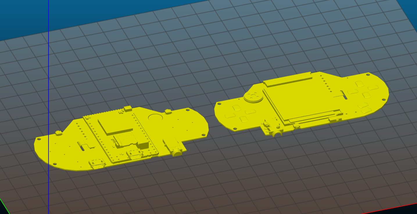
Seriously, here is an example print for the FunKey Zero PCB assembly which is everything but flat:
![]()
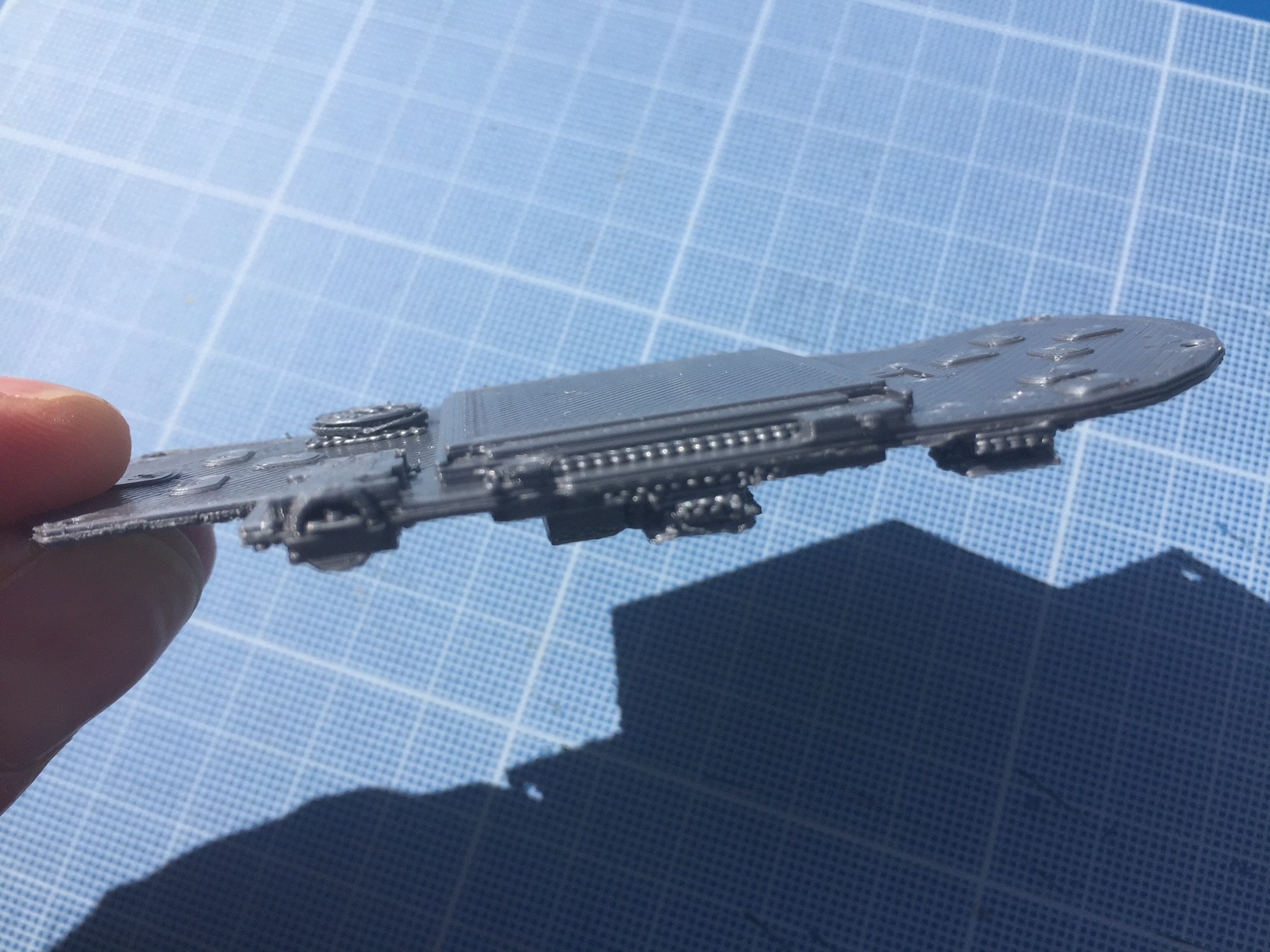
And here is how it is actually 3D-printed:
![]()
You can then assemble the 2 halves using Loctite glue to obtain the final complex part while still respecting very precise dimensions.
We did the same for the top & bottom part of the enclosure, resulting in parts that have many details both inside and outside with no visible flat surface (the glued joint plane is almost invisible and with an added thickness so small it's indistinguishable).
Let us know what you think of this idea and if this is helpful for your projects!
 c.Invent