Our journey has long left the mere "reservoir" part behind. Sometimes it appears things are growing into each other, often displacing features, sometimes acting synergistically.
This time the reservoir housing has become something between an enclosure for reservoir, pump and controller, a holder for the reservoir vessel and a fancy desk lamp. The scale / strain gauges aren't integrated at this point but we'll get there in due time.
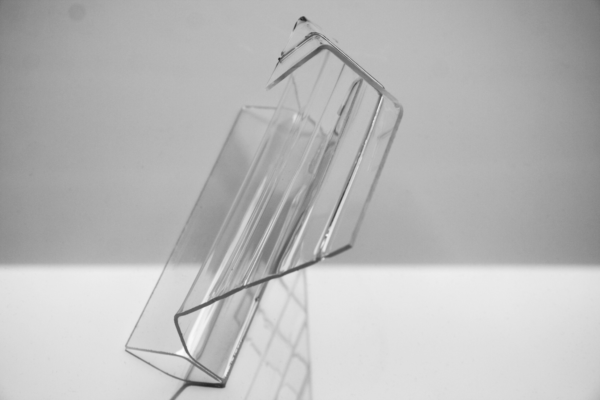
Note this prototype has been implemented with translucent PMMA while later version will be made from opaque white PMMA. With the lights out, the thing still looks rather shiny:
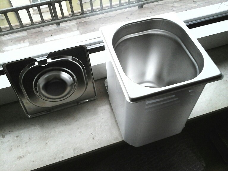
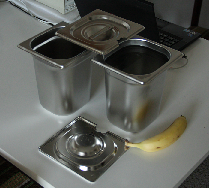
The wide open and simple lid should make pouring in without spills an easy feat. The food safe stainless steel vessel is a GN 1/6 200 mm container holding up to 3.4 L. It's a multi-sourced standard part and the dimensions are more or less guaranteed. They also come in translucent plastic.
White PMMA is a much better diffusor. Here are the rough target dimenions of the part estimated from measurements and later confirmed to almost perfectly fit the container (note the circumferential step, the mantle has to sit behind that.
Bending PMMA
I was about to say the rest is as easy as bending PMMA in shape. In practice we built the strip heater first, created bends on 3 mm test pieces (same thickness as the mantle) and measured the resulting inside and outside lengths of the specimen to base the model on them.
The bending device consists of a 600W IR heater (~45cm in length) occluded with aluminium T profiles and a flat profile wrapped in Al foil and tape in a haphazard attempt to control convective heating of those rails. It works for now but requires cooldown after each bend, so consider a water-cooled solution.
but there is no straight-forward way to calculate yielding under compressive or tensile strain in a part transiently heated from one side.
PMMA glass transition temperature Tg is at 105 °C
PMMA melting point(?) is at 160 °C
Anything between these temperatures is fair game for bending. with a distance of around 20 mm from the quartz heater and the rear reflector still in place a heating cycle time of about 2 min 15 sec (starting cold with no pre-heat) softens the material on one side sufficiently and seems to keep the other side near Tg so it will yield only slightly,
Initially a "compressive yield bend" - towards the heated side - was intended, but due to a minor oversight the first bend was made the other way ;-) As it turns out the "tensile yield bend" doesn't produce an unsightly wrinkle but slightly lengthens the material, once again owed to the inhomogenous thermal profile throughout the thickness of the sheet.
With a bit of over-bending (about 10 .. 30° held for 1-2 sec) springback is eliminated. A right angle fixture is mandatory to control the resulting angle and the 45° facet is eyeballed and tweaked in the early moments of cooling.
Minor adjustments are possible by re-heating one bend line at a time, all the while softening is tested by observation and feeling how the part reacts to slightly bending the zone back and forth.
The unfolded surface has been designed in OpenSCAD, adding small notched that help aligning the bend line to the heater slots with two drill bits. Works a treat.
The OpenSCAD export to .svg has been used to create suitable files which, once checked and modified for proper scaling are fed to the lasersaur web interface.
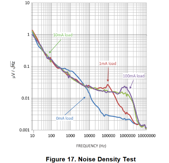
As found previously both bypassing the internal reference as well as providing proper output capacitance goes a long way in silencing LDOs. The improvement from no bandgap reference bypass to 100 nF is significant and about the same is gained by using a large 100 µF capacitor on top of it (e.g. F930J107KBA ). It has to be determined experimentally how much improvement is needed here in the context of other noise contributions. One can start out with maximum capacitance and investigate individual noise contributions one by one.
It will be annoying to add a temperature sensor to the load cell, e.g. by glueing an NTC to the element and judging by our previous set of experiments the single point load cell type does not seem to be overly sensitive to temperature variations and satisfies temperature stability requirements without further compensation and software calibration. Absolute measurements however are degraded by reference drift:
An HX711 next to substantial heat sources (such as the NodeMCUv2 board with 5V-3.3V LDO) in an enclosure will likely see a 10 .. 20 K temperature rise. Additionally the on-board DCDC might contribute with lateral heat diffusion when in operation. Counter measures include distance, thermal isolation slots and use of software calibration based on digital temperature sensor readings, e.g. from
TC74, AT30TS74, TMP100 (cheap to expensive)
temperatue effects
Once again it's easier to not cause disturbances than to deal with them later on.
I'm not especially happy with the results. Subsequent tests showed that it improves accuracy somewhat, but not as much as I'd hoped.
Once more we'e left with the need to perform more experiments to see where the 80-20 trade-off is. Maybe we're already there, or maybe integrating HX711 and subjecting it to heat and switch-mode converter noise will be a big deal.
next up we'll finally use HX711 data to determine the effects of PNP transistor selection, output bypassing, reference bypassing and power supply ripple rejection.
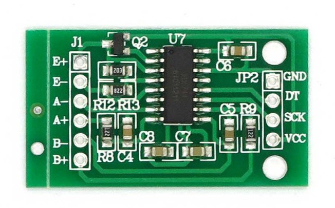
Having a look around for layout recommendations initially chips like MAX4196, MAX1452 and MAX1455 cropped up - preamp and signal conditioner ICs for strain gauge measurements. But that's a bit beside the point so here's just a reference for further reading.
While HX711 provides the same features (except the datasheet doesn't go into detail as to how the 50 / 60 Hz suppression is implemented, possibly due to patent issues) - it expands the capabilities by adding an input multiplexer with different gain options, a bit-counting command decoder for the new config options and sadly eliminates both the filter / bw limit capacitor after the PGA stage as well as the differential reference input.
ADS1231 relies on an external voltage reference and implements sleep mode with a low side switch while HX711 has an integrated LDO with external PNP pass transistor and its power-down capability.
general LDO noise
Since we're talking 20-100 nV precision it's very interesting to see this seeming neglect of differential reference implementation in the HX711 design. ADS1231 design choices also seem to hint at a possibility that integrated LDOs are usually not good enough - even dedicated external "ultra low noise" LDOs like http://www.ti.com/lit/ds/symlink/lp5907.pdf still feature 10µVrms (10 Hz .. 100 kHz BW, *with* 1µF output capacitance?) with a substantial 1/f-noise contribution in the 10-100 Hz band
This leads to suspect that just hooking up excitation and AVDD to some LDO will in both cases not be enough for proper performance. Capacitors themselves contribute some noise (kTC noise https://en.wikipedia.org/wiki/Johnson%E2%80%93Nyquist_noise#Thermal_noise_on_capacitors ) and depending upon the dielectric possibly some piezoelectric noise as well (hopefully no pyroelectric effects though), but bigger is essentially better here, as long as the LDO doesn't go unstable.
LDO stability has to be ensured via output capacitor selection - both capacitance and ESR must be in a certain range and the input capacitor should match the output capacitor by some factor (stick to typical ratio from datasheet). Larger capacitors can be added when they are decoupled with R or L elements but resistors will again contribute some noise ( https://daycounter.com/Calculators/Thermal-Noise-Calculator.phtml : 5.185k: 346 nV vs. 667R: 117 nV) - and regulation and bandwidth are not preserved. When using inductors, resonances have to be controlled by adding RC series elements. Implementing an RC pi filter is very similar to adding an output resistor to an opamp to re-establish stability in capacitive loading scenarios.
the primary noise source of an LDO is its reference, so proper bypassing of the voltage reference pin might be just as effective as increasing the LDO output capacitance. This is particularly relevant for HX711.
As for the PNP transistor...
Where to go? The individual noise sources are both defined by device characteristics and operating point. We can only change the excitation voltage to some questionable extent and we can't do anything to reduce "source resistance". What can be done however is selecting a transistor model with a higher current gain h_fe, thereby reducing base current and its associated current noise. Obviously a moderate collector current can sometimes improve the noise figure (how much SNR is degraded when the transistor is used as an amplifier) https://www.uio.no/studier/emner/matnat/ifi/INF5460/h16/undervisningsmateriale/f8-1p.pdf https://leachlegacy.ece.gatech.edu/ece6416/f09/ece6416_f09_exp04.pdf
select high current gain transistor, esp. at the ~mA operating point of the load cell excitation, keep in mind one can also parallel transistors in an effort to change the noise figure?
check susceptibility to temperature differentials (in that regard maybe also not having the LDO power transistor onboard the ADC chip has its benefits)
a quick chat with a mixed signal ASIC designer
Some recollections from a discussion with a chip designer. There seem to be some intricacies that determine design decisions. It would be really interesting to figure out the process in which HX711 is being produced. It ought to be easy to implement the 24bit ADC and integrate the LDO on the same die when using a BiCMOS process and proper guarding (gory details see http://www.iue.tuwien.ac.at/phd/puchner/node48_app.html ) whereas other less evolved semiconductor processes will not allow this degree of mixed signal and power integration. The supply voltage range of up to 5.5V is a hint, but not definitive.
Regardless the technology it always requires critical assessment whether it is allowed to place a heat source on the chip, causing analog circuitry parts to drift around as the device parameters and operating points of individual transistors change. So offloading the LDO power stage might be more beneficial than going for more complete integration.
It may well be that ADS1231 achieves superior performance by using a fully differential ADC architecture. Once more it feels like the HX711 designers made a few daring simplifications. A test to expose the quality of the ADC would be to assess integral non-linearity over the input range - ADS1231 is specified to deliver +/- 8ppm INL while neither "INL" nor "linear" are mentioned in the HX711 datasheet.
Depending on how the VFB input stage is implemented (e.g. CMOS gate) the feedback divider impedance, being the source impedance to that pin, may affect the regulator noise characteristics. HX711.VFB input current is not specified and needs to be measured to clarify.
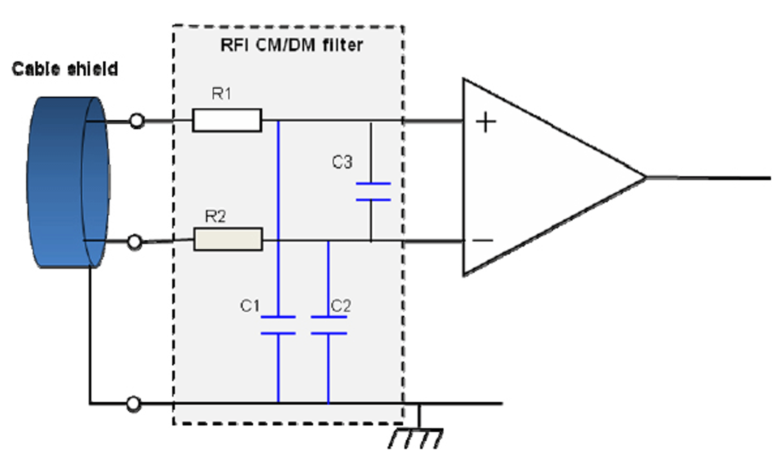
Everything below 120 dB common mode rejection is not so great - and HX711 is only quoted to have around 100 dB, with no mention of frequency or bandwidth. This suggests improvements are possible by connecting DVDD straight to 5V or another 3.3V rail, passing filtered 5V to an LDO with good supply ripple rejection, dropping down by 0.5 .. 1 V and dropping yet again to 3.0-3.5V for strain gauge excitation.
Input CMRR would also need some help by adding proper combined common mode and differential mode filtering.
To keep things simple and acknowledge part variations in cheap capacitors, the differential mode input capacitor should be significantly ( say 2 orders of magnitude) larger than the common-mode caps (think 2x 1..10 nF w.r.t. 1 µF differential mode).
kTR noise of the voltage divider should be a minor contribution to regulator noise but it still provides a means to adjust the DC current through the pass transistor if there is still some room for noise figure improvement.
final thoughts.
The few simple things I could add to it thus far would be that it might also be worthwhile to add series termination resistors to the digital lines - or even a quad resistor array with RC T-filters to control slew rates and at least test the internal RC oscillator vs. an external precision clock source.. or maybe even add some jitter for testing purposes.
The worst thing about HX711 might ultimately be its input offset drift of 200 µV at x128 gain. Hey, it has a secondary input which might be using the same gain stage! (not with full conviction because gain options for the two inputs are mutually exclusive). Maybe connecting input B pins via resistors to VBG (which is within the valid CM voltage band) might serve to measure the input offset observed after the muxer?
ps.
forget what I suggested about input B being connected to VBG. If the offset voltage is the same (proportionally) it would make a lot more sense to hook input B up to input A with INP and INN reversed.
Yet another way would be to use a SPDT or DPDT IC like DIO3712LP10 to reverse the differential mode component of the sense signal by flipping excitation polarity. Still cheaper than an HX712 ignoring availability issues :)
There's a lot of room for paranoia when stepping from the digital domain with its noise margins, supply ripple and voltage tolerances into areas of analog and mixed signal circuitry.
Connectors, analog switches, scaling networks, voltage reference and supply filtering components are situated in the analog domain while dedicated ADCs and controllers with integrated multiplexers, programmable gain amplifiers and ultimately ADCs are mixed-signal ICs.
Suddenly there are concerns about internal electromagnetic compatibility, identification of sources of - and ways to mitigate - interference. There are also selected aspects of systematic measurement errors which will not be discussed in this log (temperature effects like bias current / voltage shifts, reference voltage drift, thermoelectric voltages; mechanical effects like strain hardening, yielding or just creep, hysteresis of sensing elements, non-ideality of summed sensing elements and so on).
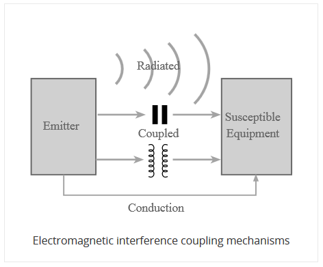
There are a few coupling mechanisms for EMI to consider when creating a new layout or fixing an existing one.
Obviously the effects - noise currents into or noise voltages added to analog nodes of the circuit (including supply rails) - are the same no matter the way they were created. The above nomenclature helps pointing at the causes of interference while looking at the interaction of electric and magnetic fields yields ideas how to address susceptibility.
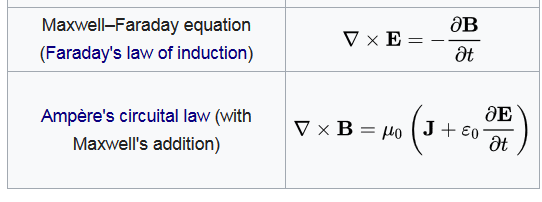
A brief detour through classic electromagnetism.
Furthermore it feels to me like the distinction between "coupled" and "radiated" EMI often doesn't make a lot of sense at the component or PCB trace level.
If part of the circuit picks up interference, it's susceptible to the local values of the electric or magnetic fields while "radiated" only suggests to me that there are electromagnetic waves involved which in turn means that one is only supposed to be concerned with field components that are able to propagate through space.
"Far-field E (electric) and B (magnetic) field strength decreases inversely with distance from the source, resulting in an inverse-square law for the radiated power intensity of electromagnetic radiation. By contrast, near-field E and B strength decrease more rapidly with distance: part decreases by the inverse-distance squared, the other part by an inverse cubed law, resulting in a diminished power in the parts of the electric field by an inverse fourth-power and sixth-power, respectively. The rapid drop in power contained in the near-field ensures that effects due to the near-field essentially vanish a few wavelengths away from the radiating part of the antenna."
Usually the near field is a complicated mess (topologically) but what matters is the net induced current or voltage. surfaces act as capacitors, loops and slots act as inductors which couple to alternating fields, constituting capacitive and magnetic coupling respectively.
Inversely, purely magnetic (loop antennas) or purely dielectric (DRA) structures work fine while predominantly coupling to one of the fields. The complementary field is being regenerated as per
But I digress. Take-away: open conductor loop areas act as magnetic noise pick-ups while free standing conductors sample the local electric field.
So "just make bad antennas". Minimize susceptible loop areas, block AC magnetic flux paths by adding ground planes and if possible arrange components to they provide Faraday shielding against electric fields (e.g. stacked PCBs or dedicated shielding cans).
Even if high frequency fields are outside the frequency bands of relevance, they might still interact non-linearly with the circuit and can thus be rectified into voltage offsets or bursts. This is where the dimensions come into play, at least in the far field and without resonant coupling effects. It always helps to make circuit loops as small as possible but where traces route to other quadrants of the PCB of off-board, splitting nets (from an RF perspective) by inserting ferrite beads and blocking interference at the inputs (both power and signal) is usually a good thing as long as peak and DC current limits are observed.
Conducted EMI
That should do for non-conducted EMI. Conducted interference luckily is more of a planar circuit-level problem once trace segments, branching and planes are properly propagated back into an augmented schematic, accounting for trace resistances and inductances.
Admittedly the intuition lives off "reading" circuit layouts and assigning guesstimated sheet resistances and relative inductances.
Tools like Keysight ADS (formerly EEsof EDA) are used to bridge this valley of subjective experience with somewhat credible numerical simulation results and help with distributed PCB and circuit element modeling.
There are three mixed subcircuits which have to be looked at in the design at hand, on top of the PCB connections themselves. Or, In other terms, everything is relevant :)
Power, analog and digital signal connections aside (input decoupling and bypassing might be in order), an SoC ADC and the HX711 are on the receiving end of whatever comes their way from the on-board DCDC converter, power connector and transients caused by the SoC itself.
DCDC converter design will have to be covered elsewhere and the SoC ADC peripheral with rather low resolution won't be too critical (that is, offset voltages , ground connection and input noise should still be controlled to a reasonable degree while being assumed to work without extreme measures), the HX711 "+/- 20mV full scale differential input voltage" worries me a bit.
minimize DCDC conducted EMI by proper layout design
minimize DCDC and SoC board coupled interference by maximizing the distance between the HX711 analog part and the DCDC zone
utilize Faraday shielding, star grounding / ground island formation
observe distinction between analog, digital and power ground zones
avoid groundplane slotting near the RF antenna, stitch top and bottom ground polygons with vias (fencing, sprinkling)
stay sane
Input power filtering might be easy to do, possibly even by plementing an RC filter where R is contributed by a polyfuse to avoid the BOM cost for additional inductors.
For the time being let's assume the DCDC is carted off to a distant location, on its own patch of ground and input as well as output capacitors tied to the one point where it connects to system ground.
Faraday shielding is a bit of a premium feature. Assuming a continuous ground plane on the base PCB and an acceptable ground plane in the SoC board this cavity should be a good place for placing the HX711. it must be noted however that board-to-board interconnects driving fast digital signals will still act as a significant source of noise. Any unused GPIO could be made an output and driven low. Due to cost optimization, the single-sided component loading implies HX711 cannot be facing away from the DCDC and SoC board. Designing for wave soldering might remove this constraint, replacing reflow soldering and some second step to solder the connectors.
Preferably HX711 is located at the far end of the SoC board, away from the RF antenna. It is not clear to what extent the high power radiation from a wifi chip antenna will interfere with HX711 - this will have to be quantified in an actual experiment with real hardware.
experimental work
Just for the sake of completeness: (All?) ADCs are influenced by converter clock jitter and there are ultimate limits to achievable "Signal to Noise + Distortion" ratio vs. bandwidth. For the not-so-bleeding-edge HX711 the external clock option is assumed to be mostly benificial to achieving a consistent sampling rate, not to improve accurary.
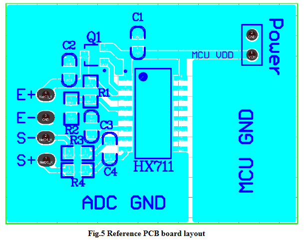
shielding has been applied after the fact and pulling both inputs to GND violates the input common-mode voltage range. Since the reference design foresees all ground connections to the analog signal ground, no distinction is made here. Keep in mind that this does not translate to being allowed to use any ground around the HX711 on a board with other circuitry.
Apart from that, there is some improvement from noisy USB to individual supply with LDO and various 5V voltage references (ADR02, MAX6350). Sadly supply noise tends to be most bothersome where LDOs fail to perform supply ripple rejection. As a general rule, both load ripple and input ripple high frequency components should be isolated from an LDO via passive filtering (de-Q-ed LC filters). Switch-mode power supplies should also be decoupled with a common-mode filter at the input.
My bet is on LC or RC input filtering without an additional LDO.
There are two more things to consider.
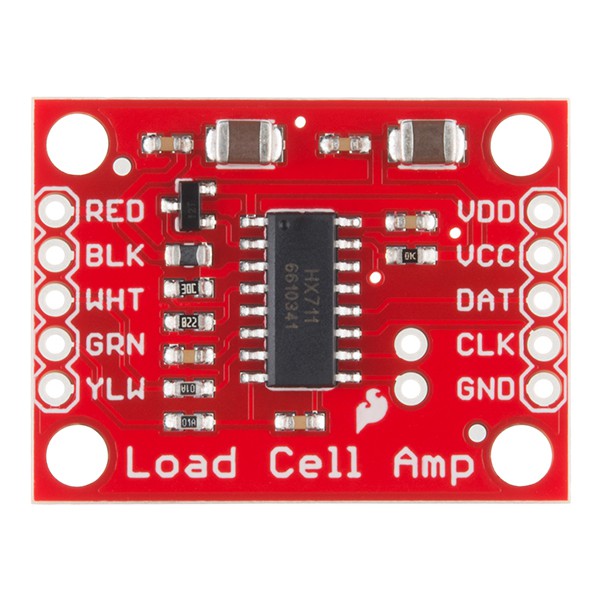
The red PCB has this weird ferrite bead arrangement which might prove performance. Additionally S8550 seems rather mediocre compared to other PNPs with higher beta and lower capacitances which may give rise to greater regulator noise.
I'd try direct connection of the pass transistor to a bypass capacitor, feeding into an RC pi filter made with a nice metal film resistor. The ADC is referenced to the same excitation voltage to compensate for scaling errors but I cannot make recommendations to which side of the filter to best connect it. Solder jumpers on early revision PCBs, go figure :)
To summarize: LDOs are not the answer, but proper supply and analog reference filtering should bring good improvements. Do use a nice patch of ground for HX711 alone and at least try to avoid capacitive coupling to noisy nets as well as magnetic coupling of DCDC stray fields.
Do test 2.4 GHz interference effects.
re ground fill:
Input filtering.
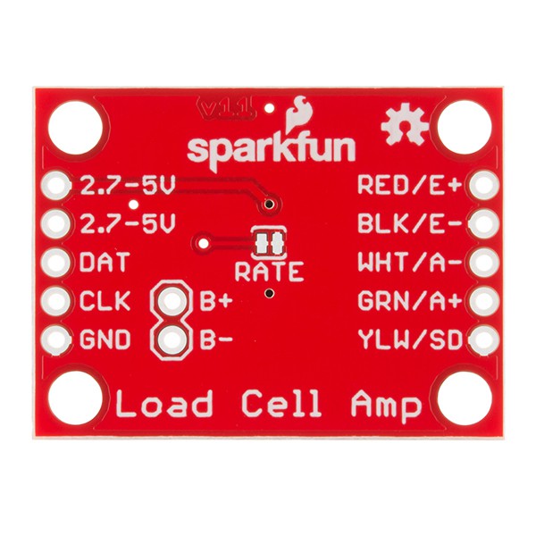
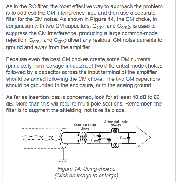
While the designers of of the red PCB at least made some effort to implement input filtering, those of the green one couldn't even be bothered to implement a proper differential mode RC filter, causing a mixing of differential and common mode components at the ADC. This is what a differential input RC filter should look like (equations see link)
and then there is the option to use magnetics. It's fun to look at for our purposes but beyond the scope of this development but it surely serves to demonstrate how far one can go. https://www.eetimes.com/document.asp?doc_id=1272503
Re power supply CM + DM filtering
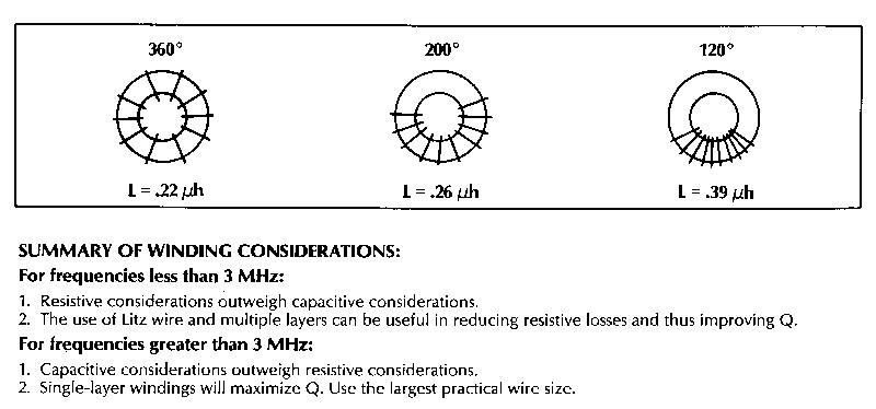
don't use rod ferrites (aka "EMI cannons"), they do pick up a lot of junk from the surroundings while radiating like mad when tasked with filtering supply ripple. single layer wound toroids (WE makes some nice ones). https://www.vkham.com/Info/ferro/tut_5a.html
The hardest part about running an experiment is to resist messing with it as it's running and there is time to figure out what things need to be changed or improved.
It's a bit counter-intuitive: A consistent measurement is better than one conducted under spontaneously changing conditions. It's easy to restart measurements when they're done within a matter of half an hour. With measurements that run for days on end it's a different story.
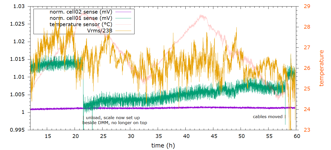
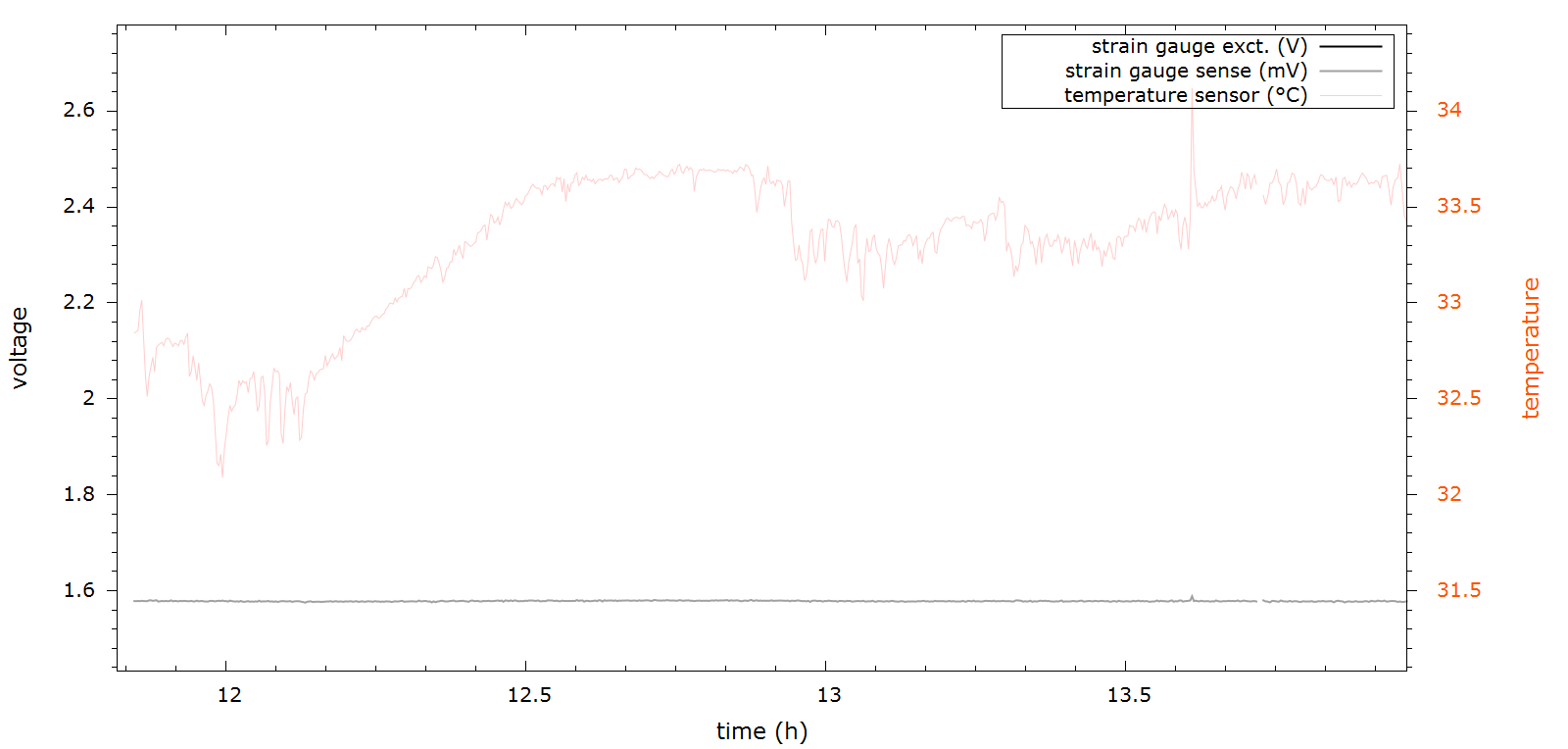
In the following graph two abrupt changes are recorded. The first one is due to the identification of a possible source of error and subsequent mitigation attempt:
suspected heating effects of the multimeter underneath the device under test
D.U.T. unloaded and set up in a different location next to the multimeter
slight slack in the power and sensing cables ensured so they don't pull on the underside of the scale
The second change was caused merely by moving the cables around a bit, causing a 0.5% jump in the reading. The change equals ~25 g load change which can hardly be explained by a few 0.14 mm² IDC ribbon cables pushing in a different way. So beside thermoelectric effects, noise pickup seems a likely cause.
A third run will use just the HX711 front ends, the scale electronics and the four pairs of sense cables will be removed to monitor just the unperturbed load cell elements.
Adding the transformer to sample mains voltage variations was still a valid idea to quantify DMM transformer + LDO loss influences and understand the other measurements in retrospect.
So on the one hand it's always worth investing a couple more hours improving the experimental setup to get better and more credible results. On the other hand, part of cunducting experiments is to identify all the things that have been overlooked or to been considered.
Say hello to these shiny 3.4 L reservoirs made from stainless steel. They're completely off the shelf and a set of those GN 1/6-200mm containers with a cut-out lid cost me about 11€. Custom made stainless steel vessels and tanks are going to be way more expensive and I love the fact that these are multi-sourced, clean-cut standard parts. Living in an area where tap water is basically liquid limestone and wanting to add a whiff of fertilizer to the water is bound to spell precipitation and algal troubles, so I'll hope to keep the annoying cleaning part for more important pieces of the kit, i.e. the tubing.
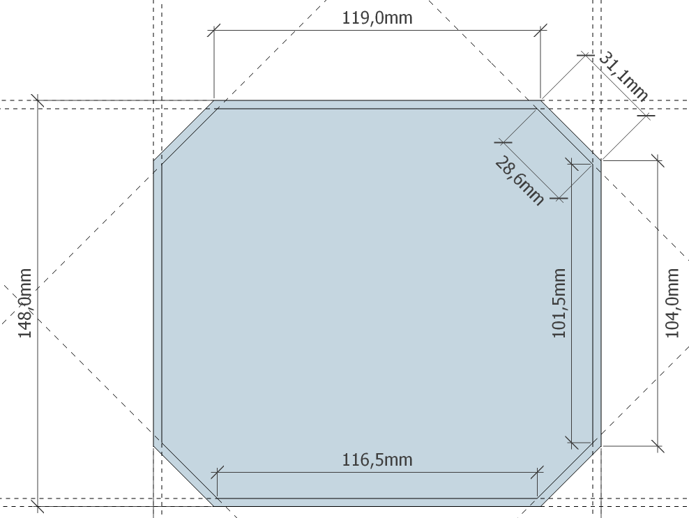
These reservoirs can be inserted into a rectangular mantle with 150 mm x 162 mm outer dimensions. Since I only have 500 mm x 600 mm stock material for the mantle this is going to be rather interesting. I'm aiming for a good fit but will add 45° corner truncations, moving them inwards by 20 mm. I've only done PMMA bending once and found it to be rather much of a pain, what with it bending back again and taking quite a few minutes to freeze in place.
More experimentation will surely be required to get the mantle right.
On youtube different versions of "acrylic bending table" builds are presented that are competing in their ability to set your place on fire.
characterize a 5 kg kitchen scale with those four strain gauges on its feet
acquire correlated measurements with the precision multimeter and HX711 via SPI
characterize drift over temperature (fridge vs. room temperature)
load cycles: 24h loaded to 100% nominal load, then 24h recovery
temperature cycles: RT (as part of the 24h no-load phase), fridge, RT (~12h each)
seems like now is the time to hook up SPI.
No precision voltage sources will be used this time because HX711 supplies the reference voltage and the measurement scaled to AVDD.
ps. single point cell - temperature drift
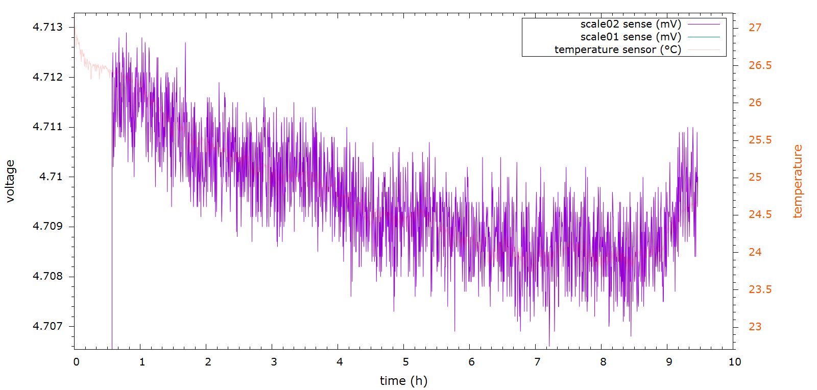
The single point cell sense voltage drift looks pretty much the same as that of the 5 kg scale elements one.
Once calibrated for excitation voltage drift however... Let's try that again for the 5 kg scale. I guess we'll have to have a look at the compensated scale01 sense voltage in the 68h run next...
pps... some time later....
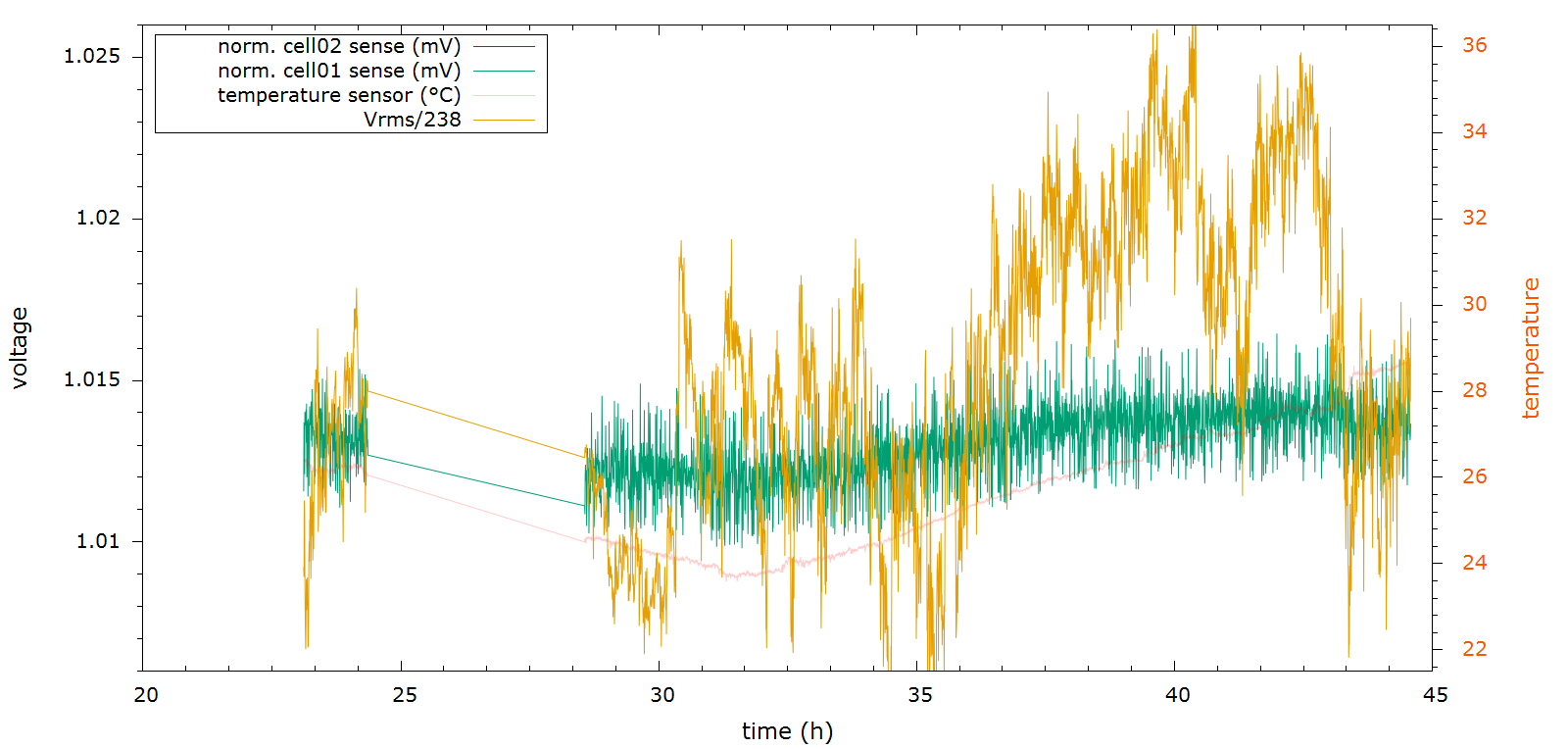
Let's look at the data again, but this time both dividing the sense voltage by the excitation voltage and then normalizing it to the starting value to display drift. With twice the acquisition time the single point load cell is still just casually walking away from us while the 5 kg kitchen scale is somewhat inspired by daily cycles. I'm not sure whether to call it a temperature effect yet.
Let's also revisit the prior long dataset with just the 5 kg scale: With the kitchen scale having an HX711 board glued onto it vs. the single point scale setup more or less floating in the air, some differences in behaviour are to be expected. Heh Sensepeek, bet you didn't see that coming. Just doing a very rough calibration of the mains voltage level it becomes evident that it's not exactly stable even over the course of half an hour: I expect some more drastic day-night variations. What's with the mains voltage? Well.. there's a transformer in the multimeter on which the scale rests, varying in heating power ... I just had to include this data channel. Next I'm pretty sure I'll also have to hook up a hot wire anemometer... driven by an HX711 board... deeper, ever deeper down the rabbit hole :D
I'm beginning to feel what it must have been like to set up the pitch drop experiment.
ppps. waking up at night
it appears I mistakenly closed the console window running the logging application when going to bed. However I woke up around 330h and found, as one does, the measurement to be terminated. A restart was in order - but I forgot about the scale switching off again. Hello, 25-30 µV offset. One might as well just discard the initial chunk of data.
Fuzzy trends: ignoring the wrong starting time for the normalized plot we're not at a point where the far-fetched mains-induced temperature variations are in the graph as well.. and they tell us... nothing? Mains voltage variation induced temperature changes are still minuscule deviations in the mW range. Maybe I'll just.. hold on a a sec... there, I just removed the kitchen scale (01) from the top of the multimeter around 1534442178.2930505. The single point cell can stay there because it's mostly thermally decoupled from the instrument and in convective exchange with the room air. The scale is again back to sleep to keep the measurements compatible with prior ones.
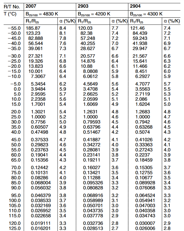
I must confess I haven't spent much time looking at NTC curves before. My prior knowledge was that they are somewhat ill-defined and can only deliver reliable measurements when calibrated individually.
As it turns out, I seem to have bought 10k NTCs of the K164 type and I don't know their R/T number. Apparently they're made by EPCOS / TDK and offered in a whole array of curve shapes / coefficients.
At first glance, 1014, 2903 and 2904 characteristics seem to match the quick&dirty calibration values:
33.6 k (sensor in plastic foil, dipped into ice slush, ~1..2°C)
10.0 k (nominal at 25°C)
0.62 k (sensor in plastic foil, dipped into boiling water ~98°C)
Mouser only seems to stock B57164K0103K052 which is listed as having the 2904 characteristics (from EPCOS/TDK datasheet above), and the datasheet only states 2904 for the 10k type.
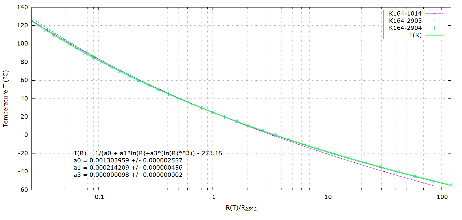
The Steinhart-Hart-coefficients can be fitted after some OCR gore as follows:
Final set of parameters            Asymptotic Standard Error
=======================            ==========================
a0              = 0.00130396       +/- 2.557e-006   (0.1961%)
a1              = 0.000214209      +/- 4.56e-007    (0.2129%)
a3              = 9.80175e-008     +/- 1.801e-009   (1.837%)

correlation matrix of the fit parameters:
                a0     a1     a3
a0              1.000
a1             -0.991  1.000
a3              0.935 -0.968  1.000
note that the S-H equation needs absolute resistance in Ohm.
There was also an error in prior graph formulas... but now the temperature calculation looks much better:
I could in principle take one of the NTCs to work and properly characterize it over its temperature range against a known PT100 element but for the sake of brevity I'm inclined to trust the datasheet values to within 2 Kelvin.
Sensors deployed in industrial applications tend to work quite reliably, until they don't. Typical failure modes include
cable breaks
water ingress and electrocorrosion
contamination with process media
range and drift (mechanical, electrochemical)
wear (abrasive, temperature cycles, cyclic bending, vibrations)
mishandling / contact with other components / machinery
voltage surges
Transferring these expectations to the reservoir scale scenario, a few points seem seem rather likely right out the gate:
cable damage / unplugged conntectors: consumer products will have cheaper cables and connectors
water ingress: sealed connectors are expensive, so unless there is some intrinsic protection against spashes, this may well be an issue
electrocorrosion: moist contamination spells trouble while conformal coating and sealed assemblies add cost. Keep peripherals powered off most of the time, only activate for brief periods. Maybe also add simple means to detect moisture if possible.
changes in full-scale value and drift: depending upon the measurement principle, yielding of metal and plastic parts is to be expected, changing the output. To be evaluated at design time.
plastic deformation: parts subjected to static or cyclic loads can accumulate strain, leading to dimensional changes and hardening. To be evaluated at design time if possible.
Assuming proper handling and controlled conditions, temperature and deformation effects can be investigated... and that's what we're going to do now.
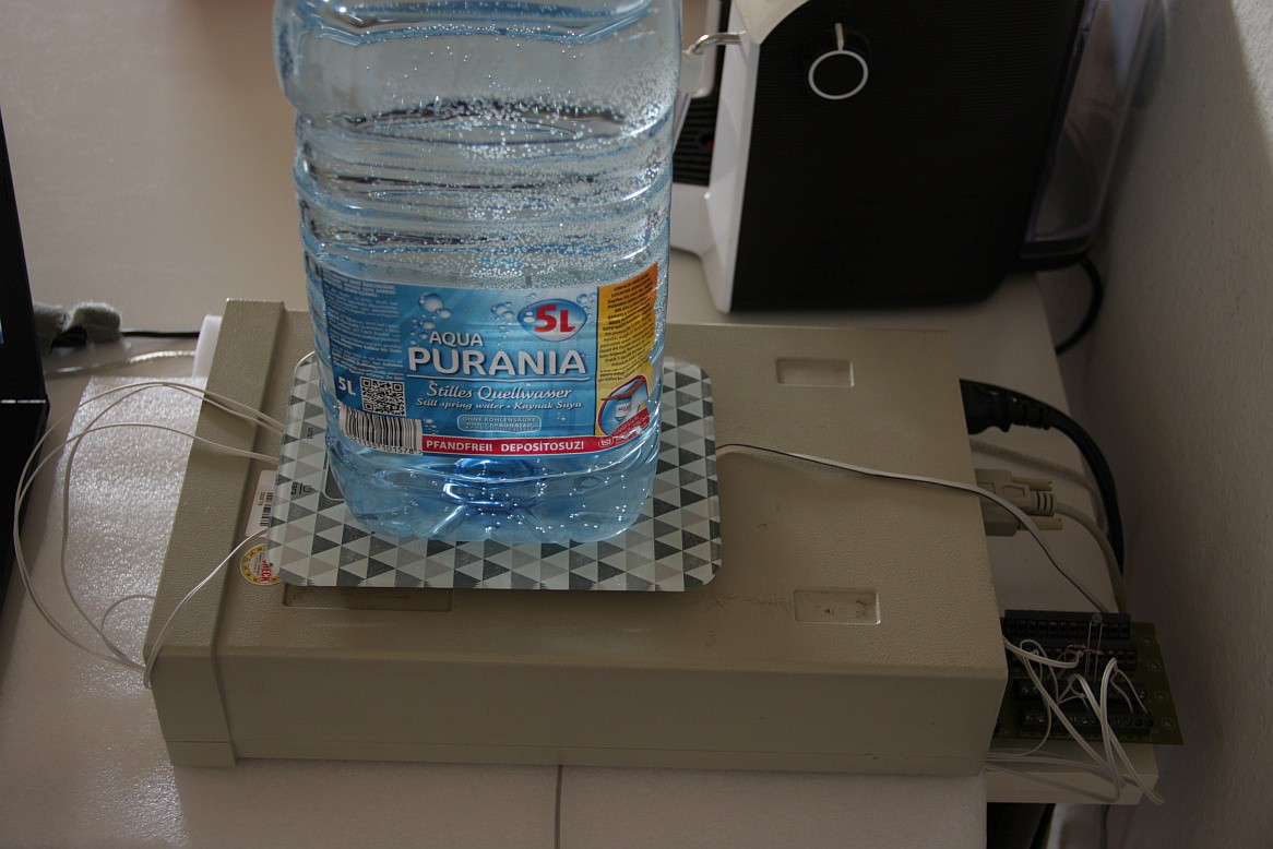
Measurement setup
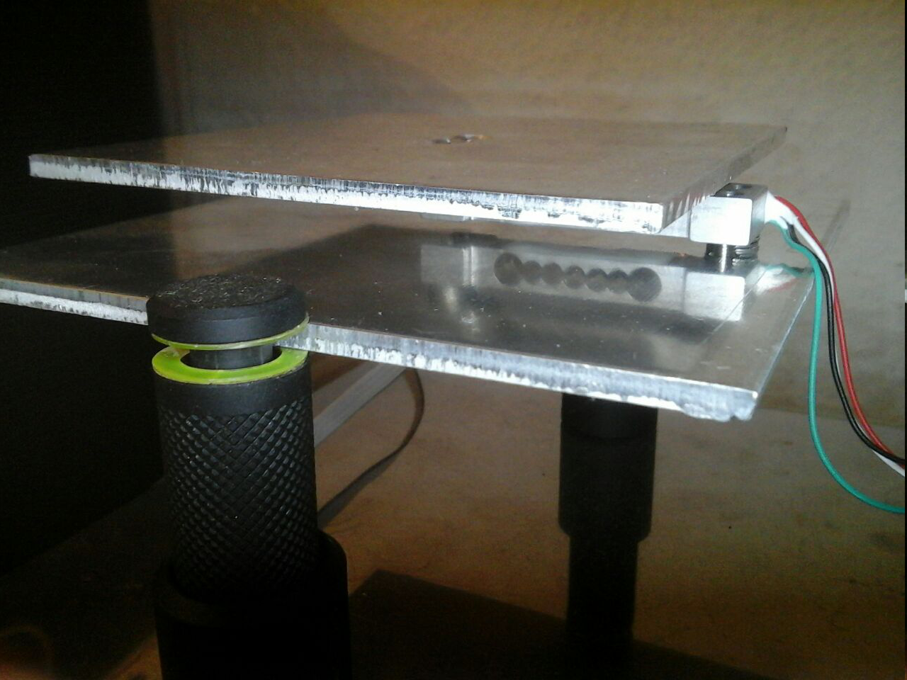
One of the modified scales is set up on the windowsill and loaded with 5kg to investigate loss of calibration after a few days of static loading with the maximum permissible weight.
Another scale with both the internal electronics and a HX711 board connected is powered with 5V into the HX711 (SCK needs to be pulled to GND to enable AVDD). This device has four cable pairs connected to the sense and excitation pins.
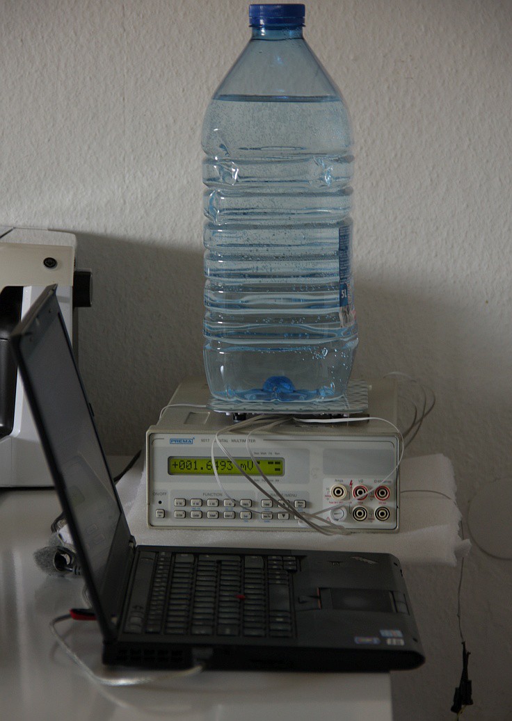
All are connected to a multichannel digital multimeter:
excitation voltage (E+ | E-)
sense voltage (S+ | S-)
partial voltage (S+ | E+)
partial voltage (S- | E+)
10k NTC (rear panel PCB / air temperature)
reference short circuit for 300mV range (same as 2.)
A rear panel PCB has screw terminals to hook up wires and an NTC sensor. In a later measurement, an additional short circuit on channel 6 was added to investigate instrument drift error during the measurement sequence.
a python script initializes and periodically reads values from individually configured input channels. Git repository:
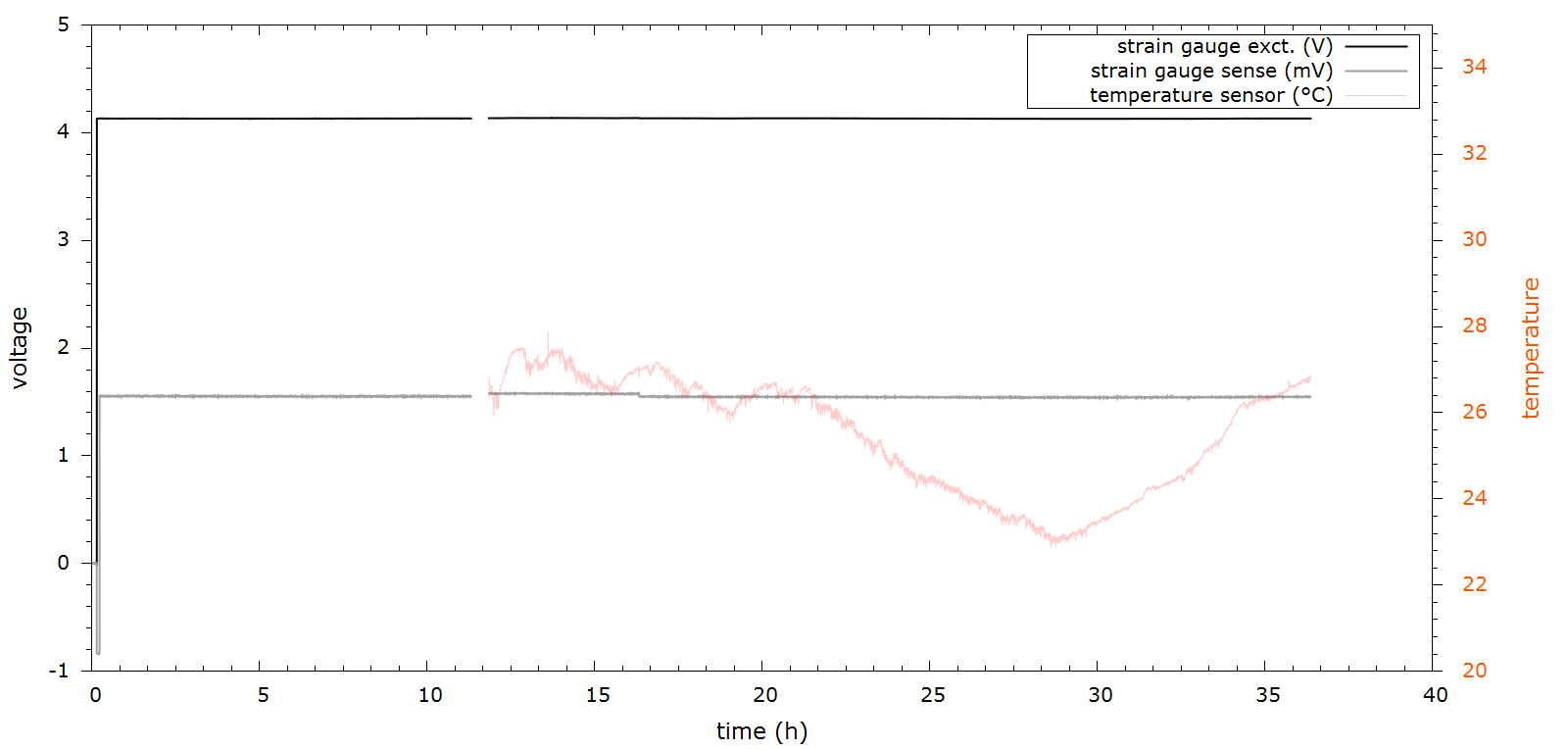
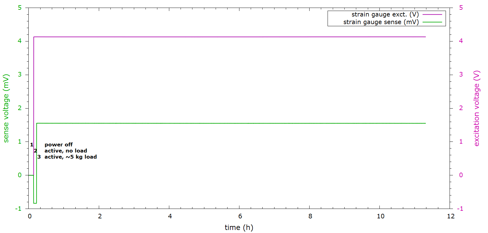
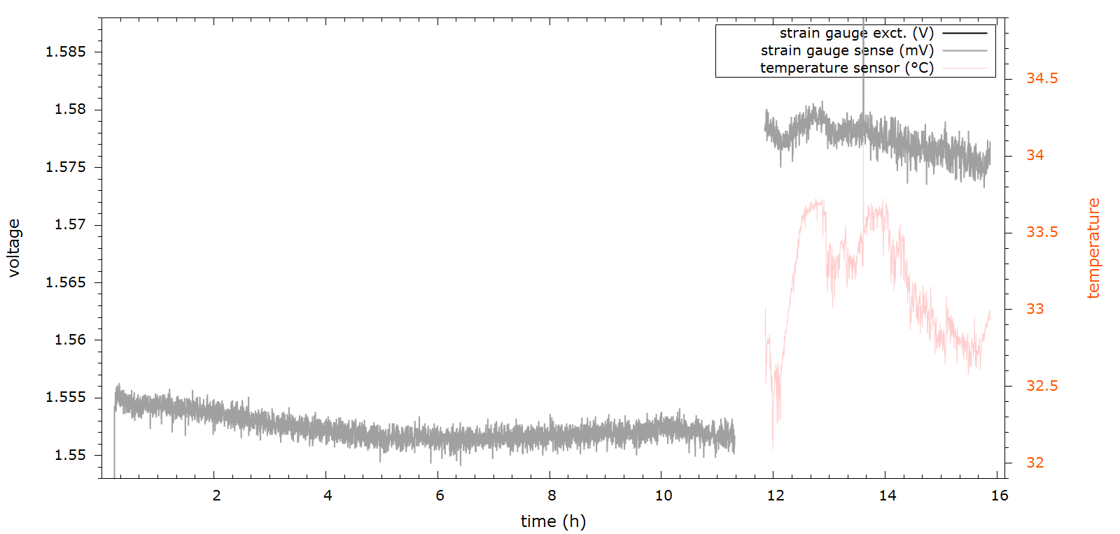
A first run is conducted through the night to determine offsets and intial settling under full load. The measurement consists of three parts to measure initial offset without any applied voltage, no-load offset of the load cell and fullscale output with a 5kg weight placed on the scale. note the strain gauge output is in millivolt while the excitation voltage is displayed in Volt.
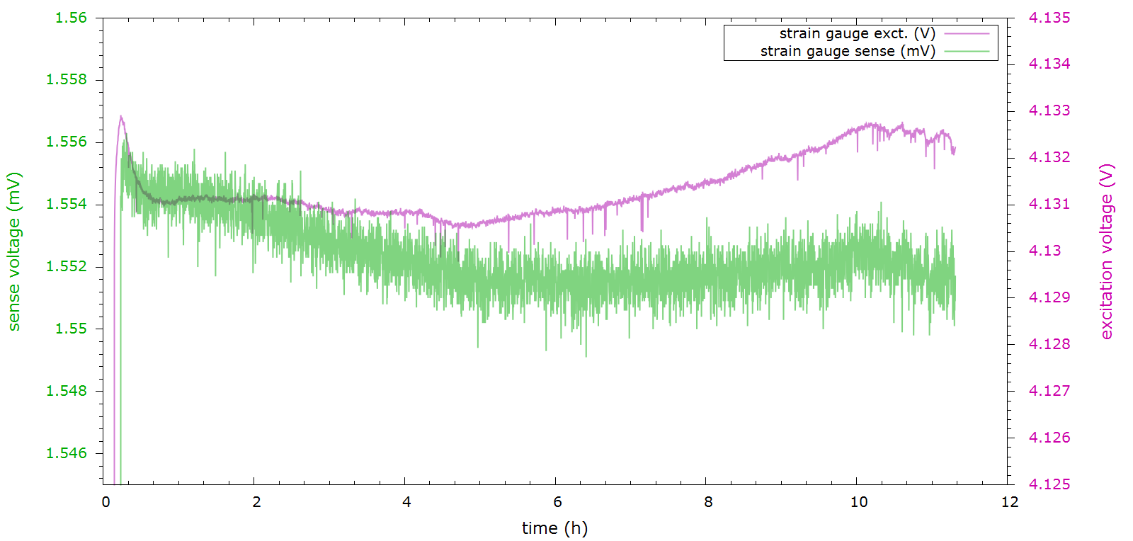
In this graph the instrument error of 74 µV has already been compensated for to better represent the strain gauge output. Y axes ranges are chosen arbitrarily to highlight relative changes over the measurement period after power-up.
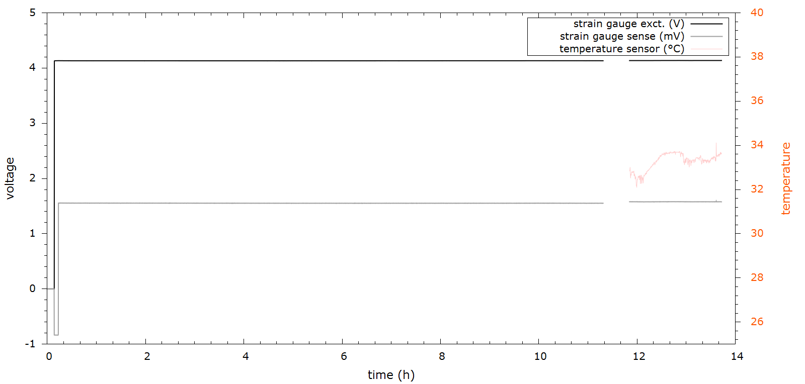
The measurement was halted to add a 10k NTC senor and test changes to the code, then restarted. Restart might cause the multimeter to calibrate zero, although it is later found that the offset remained at around 74 µV.
Note the restarted strain gauge sense voltage appears to be slightly higher than in the initial run.
There is hardly a change between the 2nd and 3rd run:
The last plot shows both sense voltage and temperature over time, illustrating the 25..30 µV jump upon restart.
To better understand temperature effects, the experiment will continue for as long as I can keep it here in the kitchen. A longer term experiment (maybe also with a stepper motor that lifts and lowers the weight) can be set up in the lab elsewhere.
Conclusion
A logging setup that monitors excitation and sense voltage of steel spring element strain gauges connected to an HX711 frontend IC has been presented in an effort to investigate drift of the sensed and excitation voltages over time and temperature changes. The extended measurement setup also quantifies drift of the voltmeter which is found to be within +/- 2 µV (1st vs. 3rd measurement). The initial strain gauge drift is found to be around 0.5%.
Based on these preliminary observations the investigated strain gauge type appears to be well suited for water reservoir monitoring. Possible sensor failure can be detected under operation when a pump removes water from a full reservoir with a known rate.
Outlook
Further investigations should also include aluminium single point strain gauges and investigate hysteresis and yield under load cycles :-)
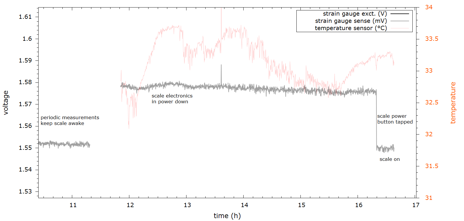
ps. auto power off
The scale electronics still connected can draw some power and possibly load the sense points differently. Now it's somewhat evident that the 25..30 µV shift is related to the state of the scale PCB and can be eliminated easily if need be.
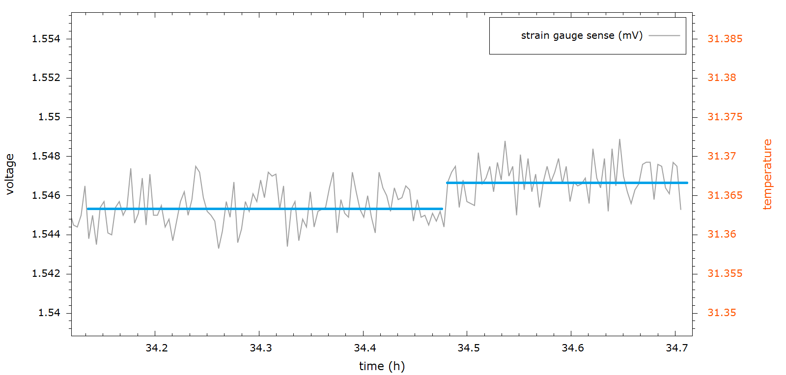
pps. : shifting the center of mass
It appears the 5L jug has been off center from the start but also inching sideways ever so slightly over the course of the day. I suppose this is due to it rocking back and forth when the table is touched. Just typing on the laptop makes it jiggle.
Since the load is shared by four cells which are summed due to the wheatstone bridge arrangement, the exact center of mass of the load should not show up in the data unless there are variations in sensitivity or hysteresis effects.
In the data the effect is barely visible and level lines have been guessed as a guide to the eye (fitting constants over intervals would be the proper way to do it).
So shifting 5kg by 3-4 cm creates a 1.6 .. 1.8 µV change. Accounting for the no-load starting value -0.836 mV of the strain gauge bridge sense voltage, a total range of 2.381 mV corresponding to 5 kg load is observed, making the observed change by shifting equivalent to a 4 g measurement error.
ppps. HX711 regulator drift
It appears the HX711 linear regulator has a thing or two to explain regarding temperature drift - if what we're seeing it not in some obscure way related to load variations by the backfed scale PCB. Also note the corrected temperature calculation. p^4s: after 68.5h, the test weight is removed, also exposing its approximate weight during resistance measurement where the wheatstone bridge is unloaded by the multimeter: "4730 g" - a new (out of the box, same type) scale shows 4672g. The people scale I bought says 4.7 kg which ain't helping. The only other kitchen scales that haven't been tampered with don't go beyond 3.5 kg.
A 1.25 L bottle seems to create 1289 g differential reading ( new 5 kg scale: 1271 g, 3 kg scale: 1273g ). so with the 1.27 kg weight we're out of cal by +1.336(4)% and +1.2414(3)% at 4.67 kg.
input loading by the HX711 ADC would tend to decrease the factor so we're left suspecting that driving the load cell with 4.135 V instead of the 2.4 V the original scale PCB would output ever so slightly voids the calibration. It's surprising though that this kind of misuse is tolerated to seamlessly ;-)
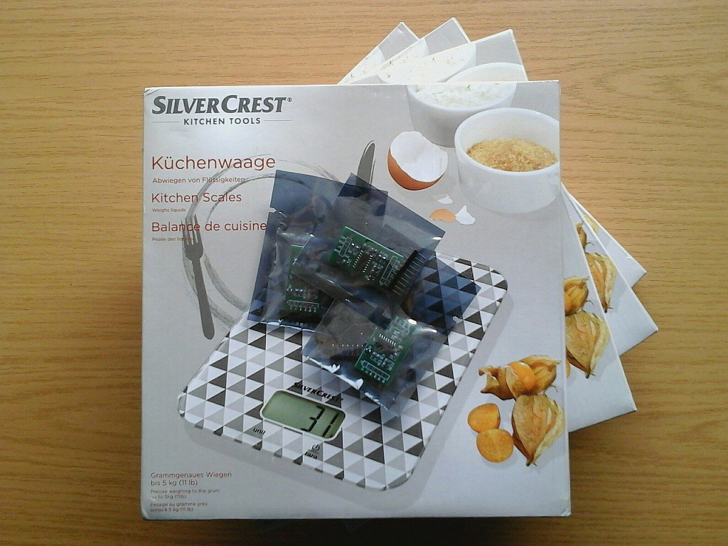
With the Silvercrest SKWD-A1 inspected and found to be nicely hackable it is reasonable to get enough scales to make it through the first iterations without yet again having to gamble and possibly ending up with a less elegant solution.
Futhermore it's hard to beat the 17 mm of this low profile scale. Buying online also made it possible to select a slightly less obtrusive pattern and colour scheme.
It is worth noting that while designs may vary over time the internal construction should be kept more or less consistent once settled upon. It also seems doubtful that there is a lot more room left for further simplification and price reduction so hopefully it'll just stay as is in the next 1-3 years.
In the previous post it has been found that HX711 enters power down when CLK is high for longer than 60 µs and a high to low transition occuring after power down will trigger a reset.
When used behind an I2C multiplexer, DOUT connected to a third data line and SCK connected to SCL, HX711 will see SCK high for a long time before selection (I2C pull-up), followed by bitbanged SCL waveforms which will be composed of the following sequences:
SCL high-to-low transition: this triggers HX711 reset, followed by a delay period during which reset is executed and presumably the first sampling + conversion with default settings is performed as part of normal continuous sampling operation with channel A and gain of 128 configured.
[ side note: Completion of the first sampling + conversion is indicated by DOUT high-to-low transition. The datasheet only states, "When output data is not ready for retrieval, digital output pin DOUT is high. Serial clock
input PD_SCK should be low. When DOUT goes
to low, it indicates data is ready for retrieval." which leads to conclude that this also applies to the first conversion after reset. ]
25-27 active-high clock pulses on SCL will read the first conversion result and set up for the next conversion with one's choice of channel and gain values.
After one or more read operations, the bus will have to revert to I2C operation. HX711 will inevitably see an I2C SCL waveform as the I2C multiplexer is reconfigured to disconnect from HX711. This is however irrelevant when the device is disconnected for more than 100 ms as any errorenous conversion will be completed by then and power down is re-established due to secondary SCL being pulled high.
The protocol co-existence described above is enabled by routing DOUT via a third line so it does not interfere with SDA. If connected to SDA, DOUT could create start conditions and lead to invalid I2C command interpretation and lockup.
If only I2C lines are available, one could generate clock pulses to trigger the DOUT high "no new data" state to follow up with I2C multiplexer de-selection but this would also demand converting DOUT to open drain with a diode or MOSFET.
Connecting it to a MOSFET and effectively inverting the output level will have further implications: as long as DOUT is high, SDA will be pulled low so the I2C bus will be in lockup during conversion and possibly also during HX711 power down (not specified in the datasheet).
Next a bit of hardware will be needed to demonstrate the functionality. Ideally the I2C peripheral could be temporarily deactivated and the pins reconfigured for GPIO. Alternatively SCL could be bridged with another GPIO configured as open drain or push-pull if it is guaranteed that I2C will not be driven in the meantime.
 helge
helge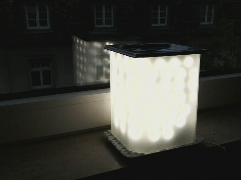
 The bending device consists of a 600W IR heater (~45cm in length) occluded with aluminium T profiles and a flat profile wrapped in Al foil and tape in a haphazard attempt to control convective heating of those rails. It works for now but requires cooldown after each bend, so consider a water-cooled solution.
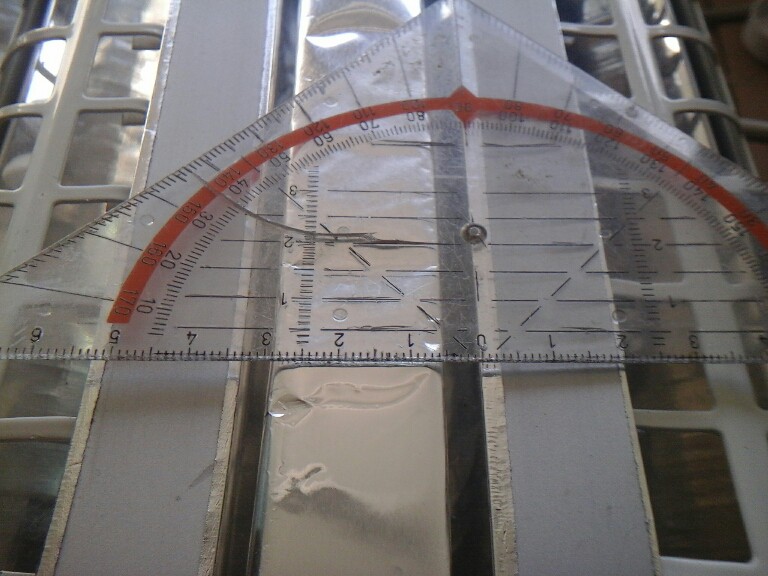
 It has to be determined experimentally how much improvement is needed here in the context of other noise contributions. One can start out with maximum capacitance and investigate individual noise contributions one by one.
 Solid electrolyte tantalum capacitors are more stable in that regard but exhibit higher leakage current.
 This leads to suspect that just hooking up excitation and AVDD to some LDO will in both cases not be enough for proper performance. Capacitors themselves contribute some noise (kTC noise
 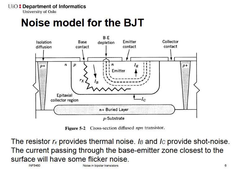 Where to go? The individual noise sources are both defined by device characteristics and operating point. We can only change the excitation voltage to some questionable extent and we can't do anything to reduce "source resistance". What can be done however is selecting a transistor model with a higher current gain h_fe, thereby reducing base current and its associated current noise.
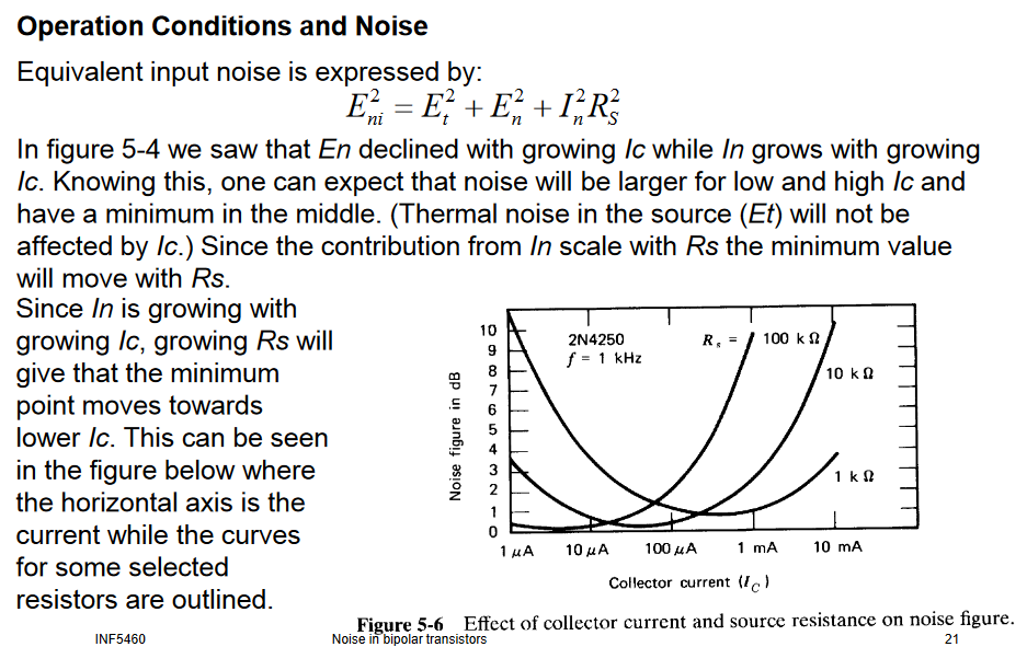
 But I digress. Take-away: open conductor loop areas act as magnetic noise pick-ups while free standing conductors sample the local electric field.
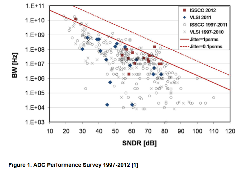
 Once calibrated for excitation voltage drift however...
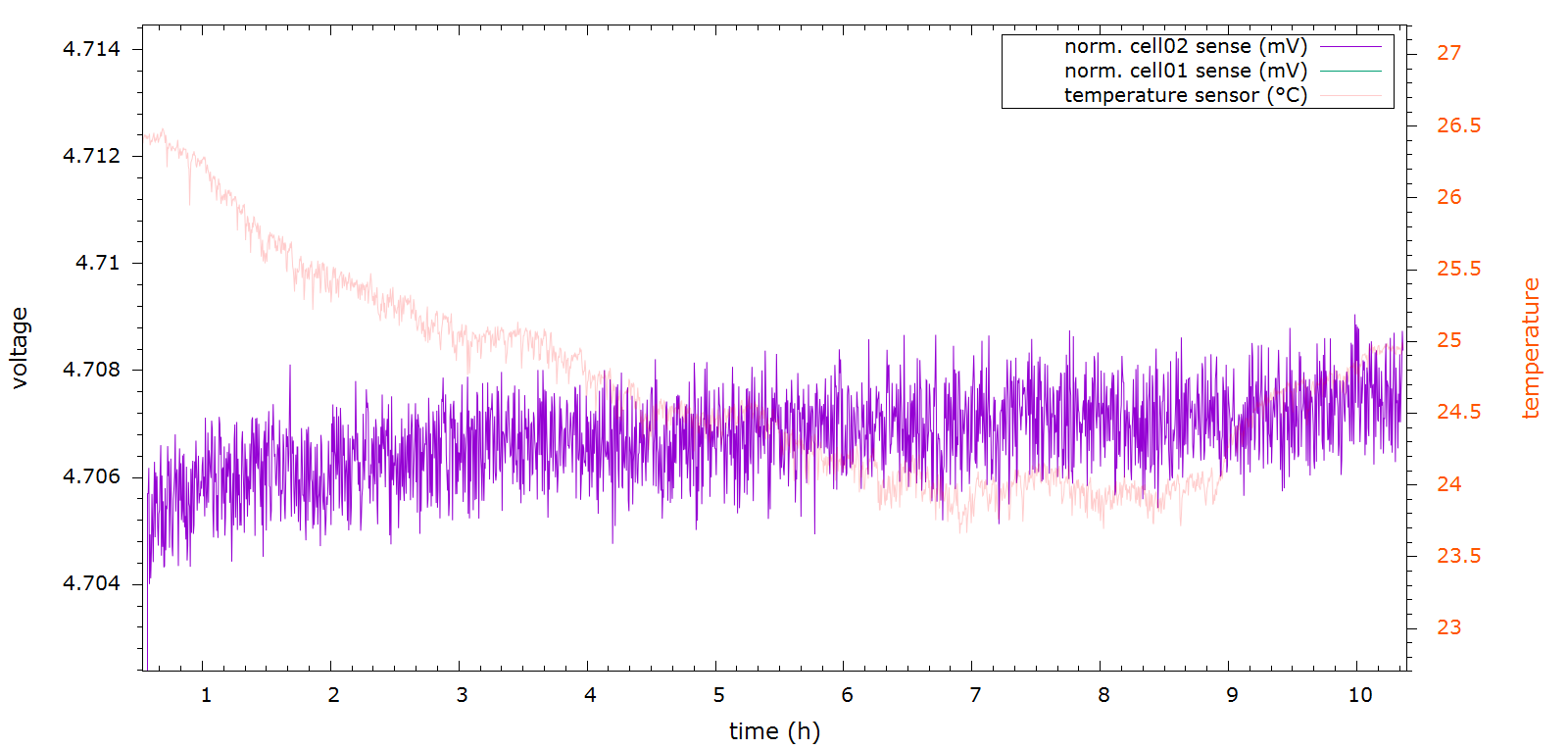 Let's try that again for the 5 kg scale.
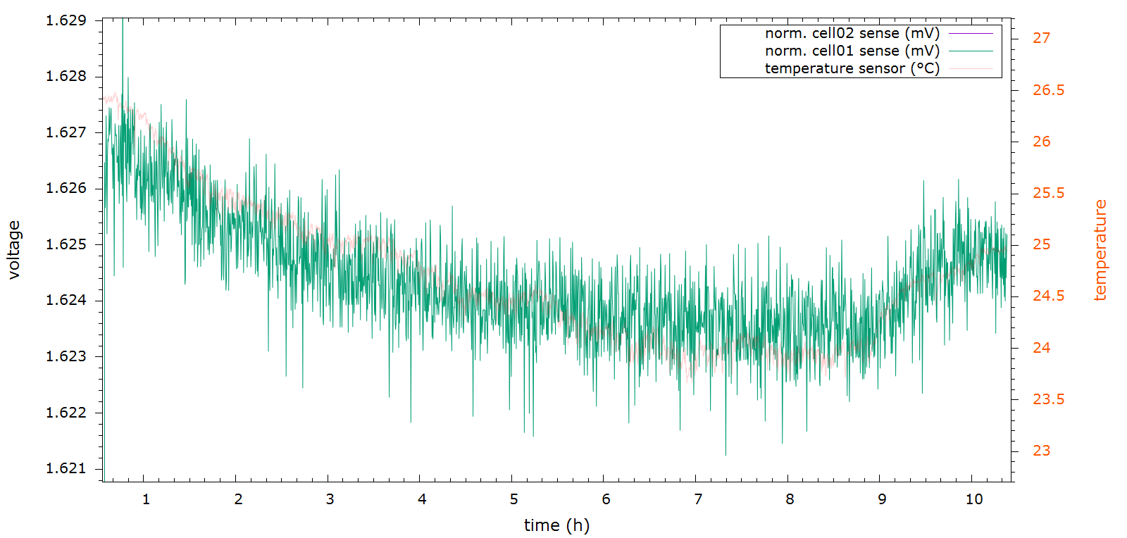 I guess we'll have to have a look at the compensated scale01 sense voltage in the 68h run next...
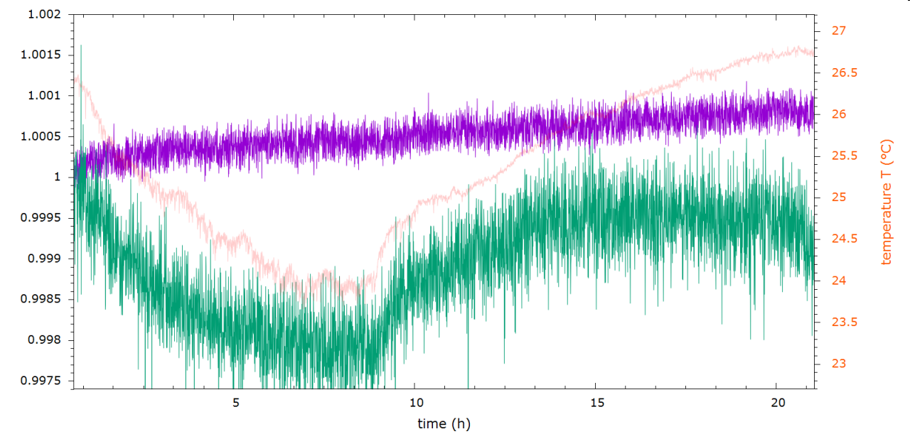 With twice the acquisition time the single point load cell is still just casually walking away from us while the 5 kg kitchen scale is somewhat inspired by daily cycles. I'm not sure whether to call it a temperature effect yet.
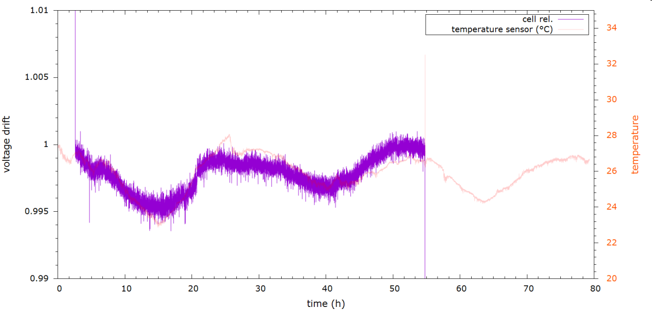 With the kitchen scale having an HX711 board glued onto it vs. the single point scale setup more or less floating in the air, some differences in behaviour are to be expected.
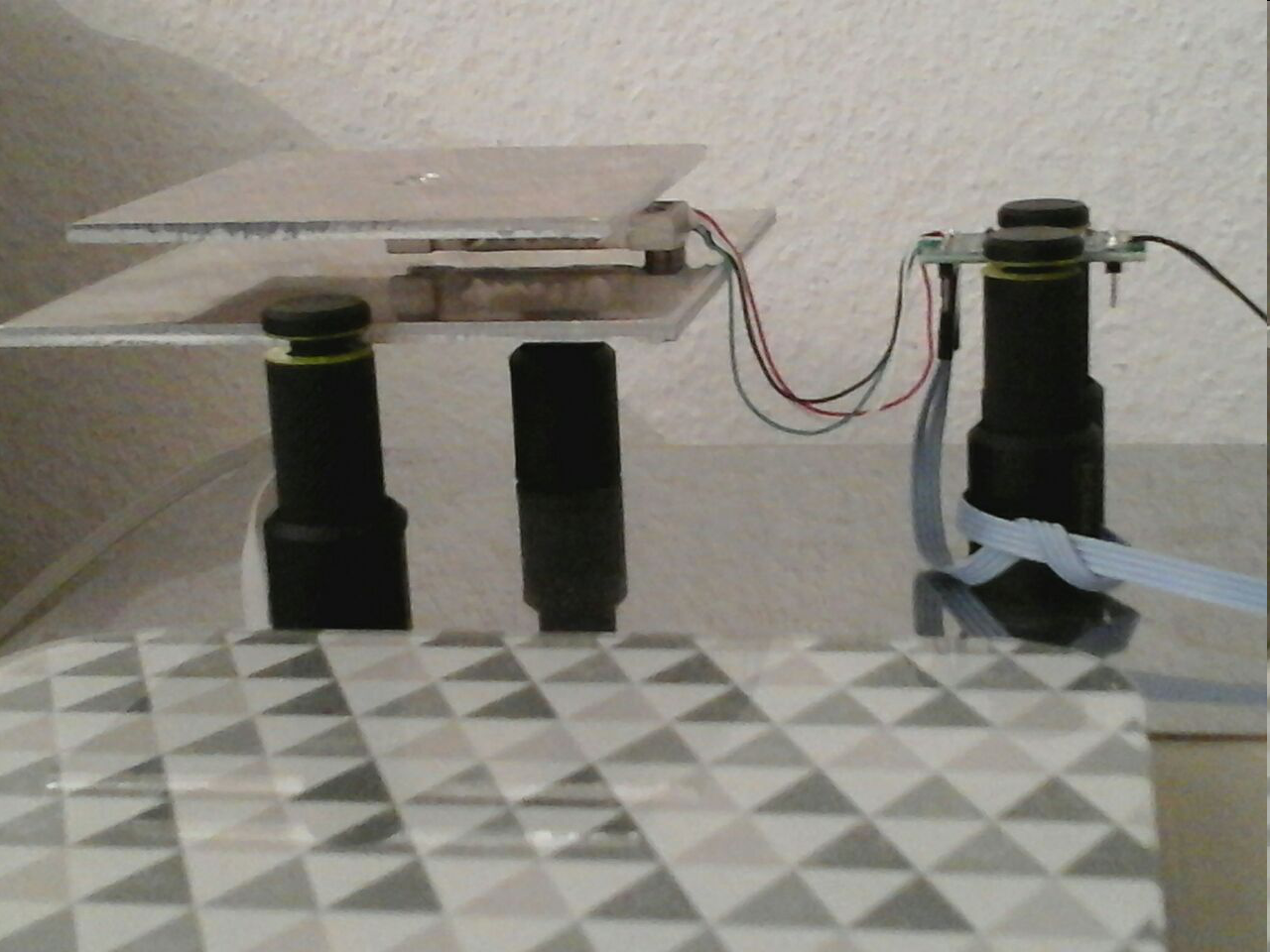
 Just doing a very rough calibration of the mains voltage level it becomes evident that it's not exactly stable even over the course of half an hour:
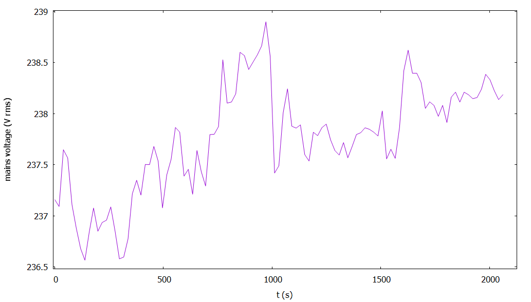 I expect some more drastic day-night variations. What's with the mains voltage? Well.. there's a transformer in the multimeter on which the scale rests, varying in heating power ... I just had to include this data channel. Next I'm pretty sure I'll also have to hook up a hot wire anemometer... driven by an HX711 board... deeper, ever deeper down the rabbit hole :D
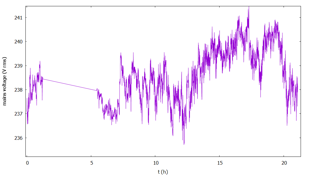
 ignoring the wrong starting time for the normalized plot we're not at a point where the far-fetched mains-induced temperature variations are in the graph as well.. and they tell us... nothing? Mains voltage variation induced temperature changes are still minuscule deviations in the mW range.
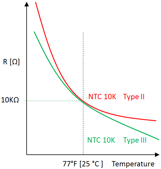
 So shifting 5kg by 3-4 cm creates a 1.6 .. 1.8 µV change.
 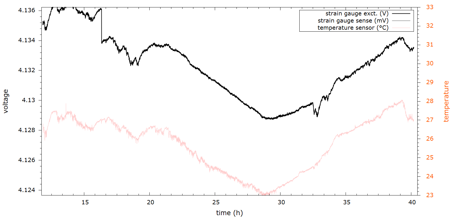 p^4s:
p^4s: