-
How to drive many relays, new version
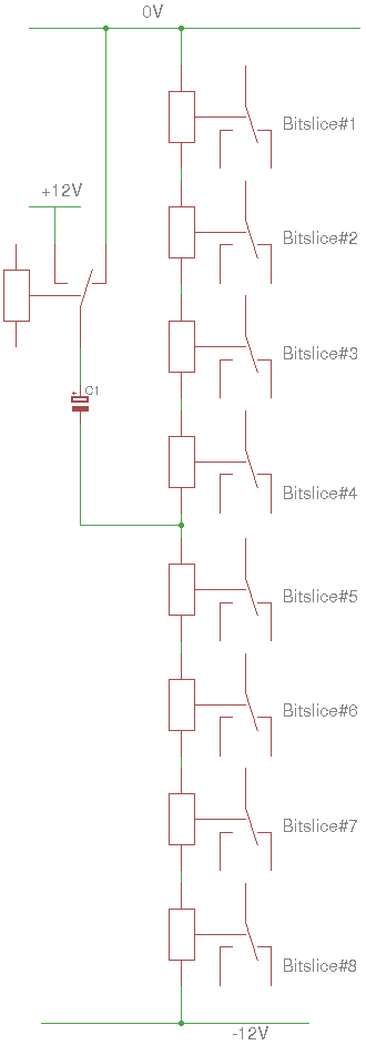
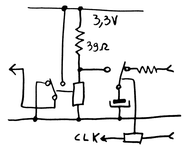
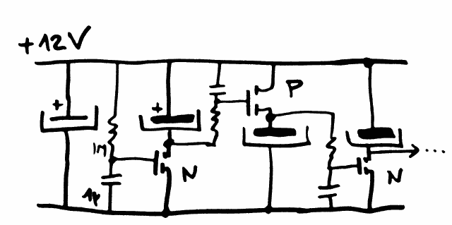
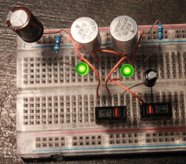
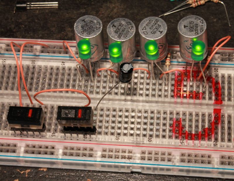
12/01/2016 at 19:01 • 0 commentsThe new CC-PBRL structure brings a new surprise. It now looks like this:
Now we have 8 relays driven by a 12V potential, instead of only 4 relays as in the previous version (shown at the bottom of My first Pre-Biased Relay Logic gates).
This is 2× more efficient but the currents and usage ratio must be taken into account. The previous circuit used a small bias current of 10mA, increasing to 60mA when active.
Now the new circuit has a constant current of 40mA per relays but there are more in series for the same voltage. This is equivalent to 20mA and now it looks more interesting for the high-fanout control signals. There is no reason to make the system more complex with "selective driving" of the large MUX of the register file. The layout and wiring are simple again.
Other advantages : the average current is much more stable (less regulation problems) a bit like the ECL. The load on the -12V/0V domain is constant (and very easy to estimate), the current spikes are mostly felt on the +12V/0V domain which draws much less current.
By the way, instead of having a symmetrical power supply, I'll use one high-power 12V PSU along with a lower-power 24V PSU.
The other advantage is nice too : there are fewer parts, only a capacitor is needed. The previous circuit was wasting power in the bias resistors.
-
What about a Game of Life ?
11/27/2016 at 14:51 • 9 commentsThe flip-dot infection has spread and there is no cure so let's go with it.
The Tetris game is a pretty cool application but then, @menguinponkey started #Game of Life on DIY TTL CPU 'S.A.M.I.R.A.' and... Do I need to explain in details ?
OK I will :-)
Conway's Game of Life.
@Shaos informed me that there is one flip-dot GoL exhibition at the NYC Hall of Science but I can't find pictures online. And it can't be great because I haven't designed it ;-)
So I'm thinking about an algorithm to efficiently compute it on the 8-registers relay computer but none of the classical computation algorithms fit. I'm one of those fools who think they can do better than Michael Abrash's awesome "Zen of Code Optimization" book.
You see, I'm a very long time fan of cellular automata. I could program one on a 286 PC with DOS's DEBUG.EXE. And I have read Michael's book. I have seen the revelations. I have applied the principles and used them in my Master's Thesis, doing interactive fluids simulations on millions of particles with a Pentium MMX PC.
I used "lateral thinking" to go 2× faster than the fastest program I could find. I squeezed it to the last cycles and developed optimization tools that boosted other projects. So I know a few things about how to compute efficiently and #AMBAP: A Modest Bitslice Architecture Proposal has barely enough resources to do it so let's squeeze again :-)
Looking back at the GoL rules, I found familiar structures that I had optimised 15 years ago, but this time it would be with 16-bits words, not 64-bits MMX registers.
Let's start with the definition:
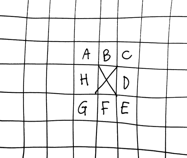
An orthogonal 2D array of bits has states 0 (dead) or 1 (alive). Each bit has 8 neighbours (lateral and diagonal).
Take any bit, call it X (that's my convention). To compute the state at the next time step, count the number of neighbours that are alive then
- If X=1, clear to 0 if the count is not 2 or 3
- if X=0, set to 1 if count is 3
From there on, every algorithm I see on the Rosetta site simply counts the neighbours. It's the definition, right ? Been there, done that, highly inefficient :-D I know I come late to Abrash's coding contest but there is a big opportunity for lateral thinking, which I successfully applied to the FHP3 model.
The key is to process as many sites as possible with boolean instructions, using very wide registers. This becomes a matter of boolean optimisation and the computation uses very few branches/jumps.
One of the annoying parts of GoL is the accumulation of the neighbours. However, with a bit of help from a different layout, it appears that a lot can be factored.
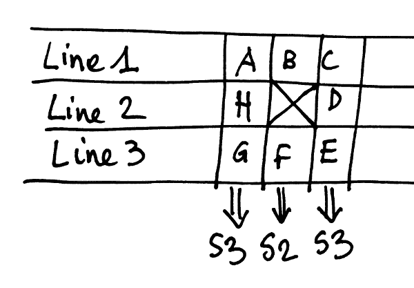
Let's define S2 the sum of the North and South neighbours. From there we can define S3 as the sum of the three East or West neighbours. If we consider that this sum can be computed "laterally", with one bit of the sum in a different register, it's obvious that we can derive S3 from S2 with a simple bitwise addition and S3 can be reused for the computations of the left and right neighbours. There is a lot of potential reuse !
Things are pretty obvious now (at least for me). The next question is : how to compute a sum ? Very easy ! S2 is a classical half-adder and S3 is a classical full-adder :-D
But now, S2 and S3 require more than one bit^Wregister to hold the 2-bits sums. Let's call them S20, S21, S30 and S31 (the last digit being the order of the bit).
; half adder:
S20 = L1 ^ L3;
S21 = L1 & L3;
; full adder:
S31 = L1 | L3;
S30 = S20 ^ L2;
S31 = S31 & L2;
S31 = S31 | S21;
With 6 CPU instructions, I have computed 16 3-operands additions with partial results !Less cycles than the number of neighbours, who can beat that ?
The less easy part is how to combine these values efficiently. A sum of 8 inputs gives a number between 0 and 8, 4 bits are required and the number of registers explodes. So let's look back at the rules.
The interesting part is when S0=S1=1 and the output is set to 1. That's a simple AND there.
The lower half of the table can be simply discarded so no need of a 4th bit to encode 8. Instead, bit S2 is considered as an "inhibit" bit.
Using this inhibition trick, the combination with the previous X state is quite easy : before ANDing S0 and S1, X is ORed with S0 to "generate" the expected pattern 11.
X' = (S1 & (S0 | X)) & ~INHNow the challenge is to compute a "saturated population count", out of full adders.Things start easy with bit 0, it's a simple full adder.
S0 = X | ( S30<<1 + S20 + S30>>1 )I include X in the computation as soon as possible so its location can be used as a placeholder/temporary variable later on :-) The register pressure is extreme in AMBAP...The destination can also use the location of the S20 operand. The left and right shifts are a compelling motivation to insert the operations just in front of the ALU. x86 will use the "LEA" instruction instead, ARM will be happy too.
S0 = S30<<1 ^ S20;
S0 = S30>>1 ^ S0;
S0 = S0 | X;
So S0 can now be located in X. But that's only the LSB and the carry is missing.
S0C = MAJ(S30<<1, S20, S30>>1);
    = ( S30<<1 & S20 )
     |( S30>>1 & S20 )
     |( S30>>1 & S30<<1)
    = ( ( S30<<1 | S20 ) & S30>>1 )
     |( S30<<1 & S20 )
I have chosen the commutative operands such that there is only one shift per instruction. The computations are basic but the register pressure it very high so variable allocation is critical. S20 will not be reused so it can hold one temporary value after being used.
S0C = S30<<1 | S20;
S20 = S30<<1 & S20;
S0C = S30>>1 & S0C;
S0C = S0C | S20;
S30 is free, now, as well. It can be renamed to S1...
Things are getting ugly now. We have four inputs, not 3, so the typical full-adder can't be used. The operands are S0C, S21, S31<<1 and S31>>1. At least, the LSB (S1) is easy to compute, it's a bunch of XOR:
S1 = S31<<1 ^ S0C;
S1 = S31>>1 ^ S1;
S1 = S21    ^ S1;
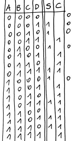
The magic happens with S1C, which is actually the inhibit signal. We don't need to compute an accurate, multi-bits result and this saves some instructions... And since we're not building an actual circuit, we can favor "long latency" over "immediate result", such that a result is progressively computed, instead of using a lot of temporary registers. But first, let's look at the truth table:
What becomes apparent is that the inhibition output is set to 1 when more than one input is 1. INH is cleared when only one, or zero, input is set. It's a sort of OR where we "forget" the first 1. There are several approaches to that but only the most computationally spartan is interesting. I decided to reuse the previous approach of splitting things into half-adders and here is the result :
The result is 1 when either the Cs are 1, or S1 and S2 are 1.
INH = S31<<1 & S21; (C1)
S1_ = S31<<1 ^ S21; <- S21->S1_
C2 = S31>>1 & S0C;
INH = INH | C2;
S2_ = S31>>1 ^ S0C;
S2_ = S2_ & S1_;
INH = INH | S2_;
There, there...
The rest is pretty straight-forward..
.
.
More algorithmics at #Game of Life bit-parallel algorithm since this project is initially a HW project :-D
-
I want to play Tetris on this relay computer
11/24/2016 at 03:02 • 2 commentsSince the idea of a flip-dot display has caught me, it appears that it would be both the most awesome and the best adapted system. It does not rely on semiconductors, it's totally in the spirit of the system and a dot matrix might be totally compatible with the DRAM system (both at the electrical level and timing, as well as the organisation). The flip-dot array could "spy" all the write cycles on the data bus, and update the dots in real time. With an appropriate address decoder, the display could be mapped anywhere in the data space so it's both a precious debugging tool (for binary lovers) and a nice framebuffer !
What's the first thing that comes to mind with such a display ? TETRIS.
If I can run at 10 instructions per second, it's still almost playable.
It HAS to be done !
The "width" must be 16 bits, with height of at least 20 (a Tetris playground is 10×20 squares). 16×24 is nice. Unfortunately the 16× width precludes the solution provided by http://www.flipdots.com/ (as was suggested by @Sophi Kravitz) because the tiles are 14×28. I am now trying to find a 16×28 array (Luminator Max 2000 or Max 3000). Any help is appreciated !
See you on this page: #Dot flippers
Update : Whatever the resolution, a Game of Life will also be awesome...
-
But what about the interfaces ?
11/22/2016 at 19:49 • 0 commentsAs I try to envision how this crazy circuit will look like to the candid users, I wonder : how will they interact with the machine ?
The machine should be more or less self-sufficient, with an electronic assembler (assembly helper) to configure the switches of a small program, and #DYPLED modules all over the place to witness the effects of each instruction.
But this is not enough: that's only my programer's side, my bias toward system development, but how could this system be used ?
It's a 16-bits binary machine that introduces basic concepts of computing. Computations fall in two major types : computational/calculations, and non-computational (as in "data shuffing"). The limited amount of memory makes shuffling hard but this should not be brushed off.
The obvious application is to play with numerical algorithms : how to compute approximations of functions, the like... this leads me to look at another project again : #RISC Relay CPU is definitely a calculator, while I'm trying to make a computer...
A calculator only deals with numbers and a numerical keypad is all that's needed, along with 7-segments digits (I got #DYPLED for this already). But can we please extend the idea further ?
I'm thinking about adding an I/O bus. IN and OUT instructions will access physical 16-bits ports where you can hook up any peripheral device you like. Maybe a serial line, external storage or a #Low-resolution scanner for cheap data input?
A dumb electromechanical keyboard is possible but I don't want to restrict its layout or purpose. And then, what about the display ? What convenient alphanumeric interface exists ? (other than 16×2 characters LCD modules) ? How is it possible to create a 16×32 bitmap display ? Flip-dots ?
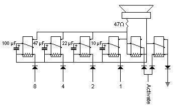
Sound is easy, though, as Rory provided the schematic of his TIM-8:
Any other idea ? -
Building a LFSR with relays
11/22/2016 at 00:42 • 0 commentsSo that's another twist of this "exercice de style" : now it's time to evolve from the ring oscillator to the Linear Feedback Shift Register :-)
I'll start with a 5-tap LFSR with poly (5,3), meaning relay#1 gets the XOR of relay#3 and relay#5. This generates a cyclic sequence of 31 numbers, excluding the number 0.
It's time to evaluate how many relays are required: each "square" or tap is a synchronous FlipFlop, which uses 2 relays: one for storage, the other for clock/control. A capacitor is used as a temporary storage.
The little gotcha is the clock : at 5 tap, it doesn't work well to optimise the power, I can make 2 DPDT with 4 relays but another relay will need a bias resistor. Hopefully, this will be addressed in the final version, with an even number of taps (or multiple of 4 ?)
So far we have 2 relays per tap (10 SPDT relays for 5 taps) but the XOR2 is not done yet. This is solved with a "PBRL-DPDT" structure as shown in a previous log.
Tap#1 needs a single data input, which is XORed by tap#3, so an auxiliary relay (the second of the DPDT structure) selects one of two inputs. These inputs are generated by tap#5, which swaps +Vcc and 0V depending on its state.
This adds 2 relays so we get the formula 2(n+1) relays for n taps. I have not counted the MUX to the address bus though, so it's on the order of 3n.
Time to build it :-)
-
Refresh logic
11/21/2016 at 23:20 • 0 commentsWith at least 2 minutes of data retention, the requirements for the refresh cycles don't look too bad.
Yet, with a "worst/best case" of 512 words to refresh every 2 minutes, or 120 seconds, that's 4 words to refresh every second. With an optimistic rate of 12 instructions per second, every third cycle will be stolen by the refresh cycles. That's a LOT and my idea to use an interrupt is now unrealistic. I can already forget about the scratch memory area, which would consume circuits anyway.
Now let's suppose I could "steal" one computing cycle every 4 or 8 cycle. The aim is to reuse as much existing circuits as possible to avoid bloating the architecture. Relays are cheap but not free.
The refresh occurs with a single instruction : increment an address register. The result goes back to the register and to the address bus, which triggers a read-and-rewrite cycle. This single instruction can be hardwired and injected in the instruction stream periodically, using a different "mode".
A "shadow A0" register can be implemented (3 relays, no need to decode 2 operands) and selected in the "refresh" mode. The increment instruction is selected automatically, "clear 2nd operand in ROP2 and set carry-in to 1 then add".
Another solution is to "steal" memory cycles, when no write to the memory is detected, so it occurs in the background, transparently. The address is generated by a LFSR, of a width that is equal to the address bus, +1 to prevent the "blind address 0" problem. Cost : maybe a bit less, this requires another MUX on the address bus, but the LFSR is not as wide as the whole system. 512 words will require 10 bits and 9 MUX (plus a little bit of detection logic to enable the address increment).
So this is another occurence today where the solutions come when I write about them :-D
The cycle-stealing idea is probably a bit sophisticated but it doesn't cripple the already poor performance. And it boils down to
- detect when no write to A0 or A1 might take place (it's not important if the instruction inhibits the write)
- create a suitable LFSR with a minimal amount of gates
The first is easy : detect when the instruction does not contain A0/D0 or A1/D1 in the destination register. It's as simple as checking 1 bit (the MSB) in the instruction "destination register" field.
The second part is a bit more heavy, as it requires significantly more relays. But it's an interesting exercise.
So we're going to make a LFSR with relays.
Let's start with the polynomials: I have written an article about them in 2009 so I have a list of minimal-XOR polynomials of relevant sizes. Look at some source code at http://ygdes.com/GHDL/lfsr4/ : there are a few polynomials that require only a XOR2 :-)
2=>1
3=>2
4=>3
5=>3
6=>5
7=>6
9=>5
10=>7
11=>9
So all that's left to implement is : a 2-inputs XOR and DFF latches.
I suppose I could reach 512 words (2^9) so the 11-tap polynomial looks good, since it will "skip" address 0 only once every 4 full cycles. Or we can just say "address 0 is the PC" and stick to a 9-tap LFSR (ensuring that the whole range is covered once and only once every 511 cycles).
The LFSR should not be 0 : 1s can be injected during the power-up sequence, or some relays could be set to power up in a set state.
Update: even-sized polynomials are preferred...
-
New challenge : power-up sequencing
11/21/2016 at 21:08 • 0 commentsThis beast is going to draw "a lot of power" and turning it on might create some significant inrush current...
I should automate the startup sequence : turn the power on for each section, one by one, then toggle all the CCPBRL control signals to set each relay to a known state.
Yesterday I figured something out with MOSFETs:
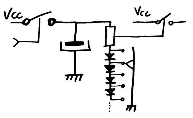
This method is nice and uses the "smooth" linear mode of the MOSFETs to prevent spikes (before going to "ultralow resistance" mode) but I have to stick to relays. The RES15 can't handle much current so I'll use a different type, but the coils consume significant current and RC delays are hard to make without LARGE capacitors. That's one conclusion from the first experiment with the Relay ring oscillator of #SPDT16: 16-bits arithmetic unit with relays.
So the problem is "how to sense the voltage" and ensure it has reached a high enough level before switching the next section. PBRL doesn't help here. But writing about it made me imagine a different system... I was simply looking at it from the wrong perspective.
So let's imagine I power several sections, for example 4 bitslices each. That's 4 high-current relays.
Let's measure the Von voltage of the power relay then add diodes in series to make the desired trigger voltage :-)
This limits the inrush current to one section, but can the current be reduced as well ?
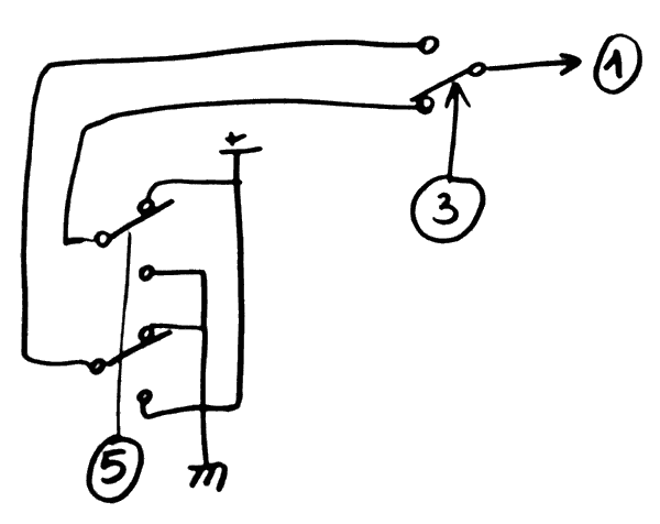
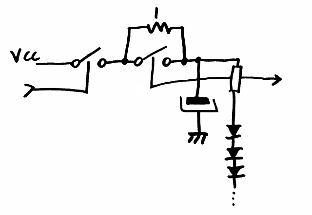
Using a DPDT relay makes it possible, the following circuit lets the current flow through a current-limiting resistor until the voltage reaches a defined point, after which the resistor is shorted.
The value of the resistor is important. I have chosen 1 Ohm to limit the current to 1A/V. I have not shown the rest of the circuit, made of plenty of 40mA sinks... if the resistor is too high, the voltage may not reach 2Vcc/3 and trigger the charge of the next section.
For the capacitors, I have "enough" 22000µF/16V and 10000µF/35V.
.
2022/02/10 : I found a way better system ...

-
Data RAM parity
11/21/2016 at 15:53 • 4 commentsIn Memory arrays for relay toy^Wcomputer I suggested that parity would be an important feature. It will help evaluate the actual data retention time of the whole array, and detect run-time storage errors.
Parity is just a XOR of all the bits, stored in an additional bit/plane of the memory array. To do this, the usual method is to make a tree of XOR2 gates. Given the propagation time of the relays, the tree would need 4 or 5 "relay times" (15 to 20ms ?) and slow the whole computer down.
Do you remember the DPDT circuit in the log Dual-voltage power supply? Well, it's not only a solution to the carry chain but also to the XOR tree. On top of that, since it's a O(1) kind of circuit, the XOR gate can be located on the bitplane: on the globule or the RAM board.
There will be one more RAM board than globule slice so the read sensor, the write buffer, the parity and such should be located on the RAM board.
Furthermore, the parity must be computed during read and write cycles, so 2 circuits are needed. That's 2×2×16=64 relays overall, or 2 boxes. But there could be a trick if speed is not critical, as the parity can be looped back from the sense relay :-) I should sketch it to be sure...
-
Data retention with capacitors
11/21/2016 at 06:25 • 0 commentsThe design of the (D)RAM is a burning issue because there are still a lot of dark corners. Today's tests raised an interesting aspect that is worth another log.
The requirements of the storage cell are
- store enough energy to flip the sensing relay's state
- store it long enough that refreshing is not a hassle
It's hard to check because any measurement will empty the capacitor and reduce its storage longevity.
But another concern is its ability to deliver its energy and flip the relay. It appears that it's not just a matter of how many microfarads it has.
So far I've been using miniature 100µF 10V electrolytic capacitors. They have proved to be great as liaison capacitors for CCPRBL but their role as storage cap was elusive. Maybe there is too much ESR ? But if so, why does it work as a liaison capacitor and not storage capacitor ?
Leakage does not seem to be a cause since immediate release of the charge is not working either.
Actual capacitance seems to be in the 200µF, as I measured it to check if it was not a bad lot. The parts are still in original bag, 5 years old at most.
Then I swapped the 100µ with a 470µ 35V and it worked.
Again, is it a capacitance issue ? I put 2 or 3 100µF in parallel (600µF) and still no reaction.
Then I tried to increase the storage voltage. A pair of 9V batteries makes a nice symmetrical +9V/-9V supply.
Well, the 100µF aren't rated for more than 10V so it's another faiilure. Whereas the 470µF works well, retaining enough energy for 2 minutes (I didn't have the patience to wait longer). I tried a 47µF 63V with success too.
If it's not capacitance, then what is the critical aspect ? Leakage can be compensated with a higher supply voltage and is not a problem since I will need to have +12V/-12V supplies. I suspect that the two other differences are the size and the rated voltage: a better insulator, maybe, helps a lot.
Yes, size matters.
I'm waiting for the 100µF 16V capacitors I ordered and I'll test them with 0/+12 swing but I suspect they are "too small".
An important side note: The circuit with the "good capacitors" works in pure PBRL mode, forcing the coils to the desired state. This means that the capacitor forces the coil to - or + (compared to the middle point) and the sense relay keeps the last state.
The hysteresis reduces the amount of switching (and wear), reduces the read/rewrite cycle time and simplifies the circuit because other options require an additional relay to "flush" the sense relay...
-
Pre-Biased xPDT relay configuration
11/21/2016 at 02:50 • 6 commentsThe 3rd drawing from the last log (Dual-voltage power supply) asked for a verification.
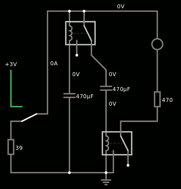
The CC-DPDT circuit works well, from 2.5V to 3.9V :-) [yes I bias the capacitor in reverse, booooh]
If it works well under 3V, there is no reason to tune the 12V power supply and I can string 8 relays ! Of course I should account for about 10% resistance/temperature drift due to Joule heating in the copper.
The other thing to consider is power-up: half of the relays are "on" while the others are "off" so at least one on/off cycle is required before the system is in a known state.
A 4-relays version is tested successfully between 5V and 7V. The capacitor is connected to either 0V or Vcc, I haven't checked the voltage influence but it makes sense to keep it that way.
6V seems to be the center voltage, though that might vary with relays. For example, two relays can't hold a value for a long period when close to the end of the range. OTOH, they are stable at 6V (not too sensitive to vibrations for example). Out-of-median specs should be paired : a higher coil voltage can be paired with a lower-voltage to create a median-voltage pair...
AMBAP: A Modest Bitslice Architecture Proposal
Trying to unify and simplify a minimal architecture for various implementation technologies...
 Yann Guidon / YGDES