David Brown
-
Design considerations - updates
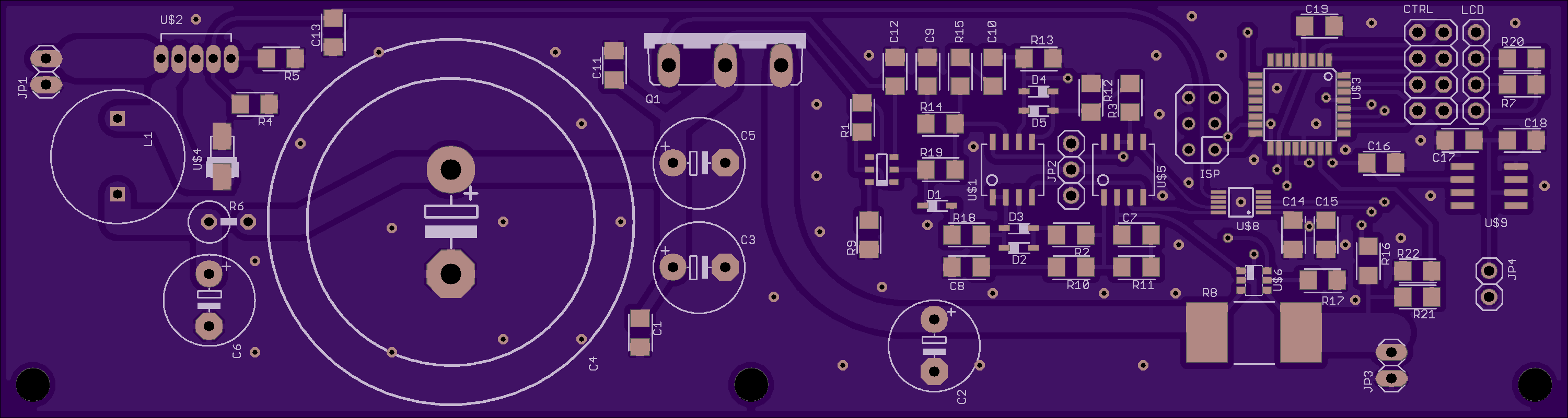
11/15/2016 at 21:55 • 0 commentsI've been reading up on a few more details of power supply and analogue design, chiefly grounding considerations; for things like ground differential, controlling where the current flows, whilst keeping it away from areas that could be sensitive to it, but minimising the resistance.
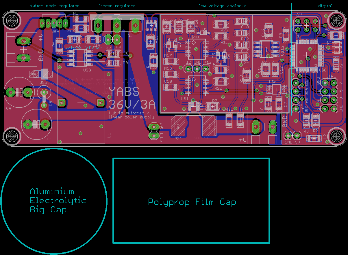
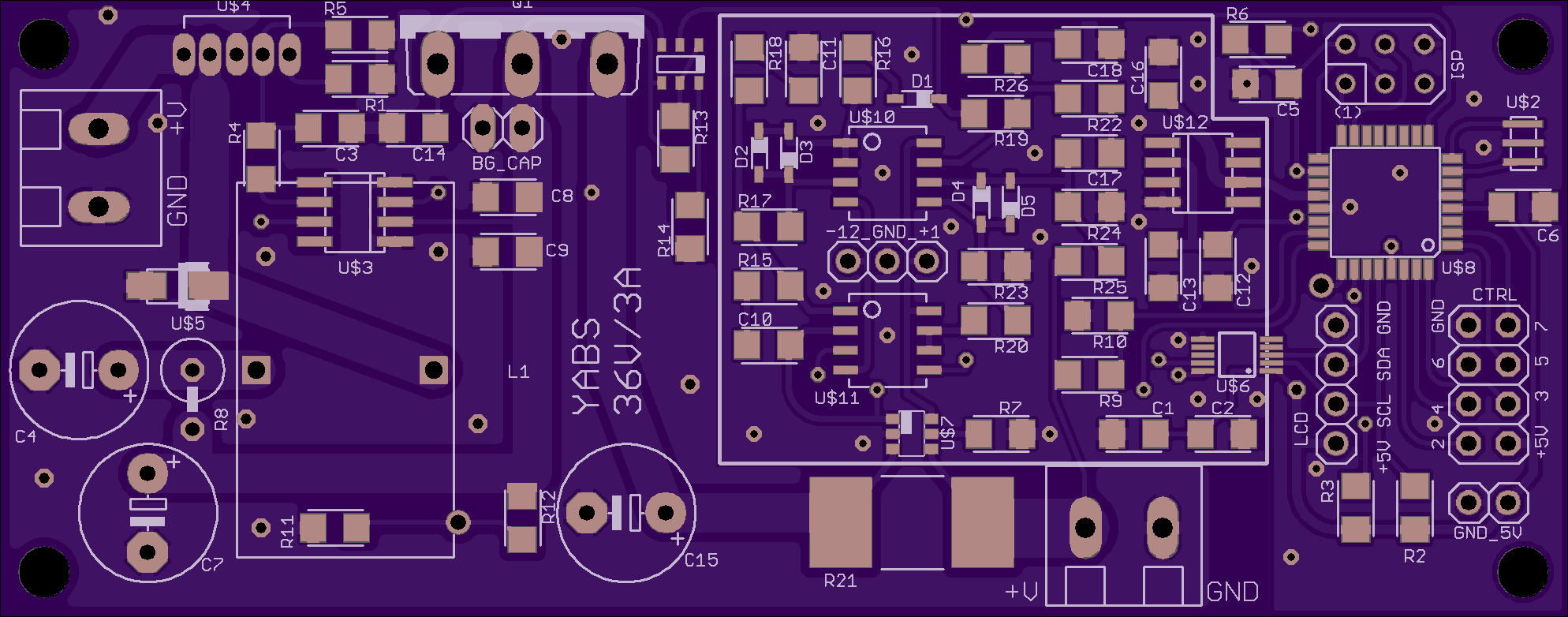
So I have been tweaking the supply board so that there are effectively four ground areas. One for the switched mode mode section, one for the linear section, one for the analogue control circuits (Op Amps one side, with precision voltage source, ATMega analogue supply and the control DAC ) and finally one for the digital section. These can be identified on the plot of the current layout, circuit posted in files section.
![]()
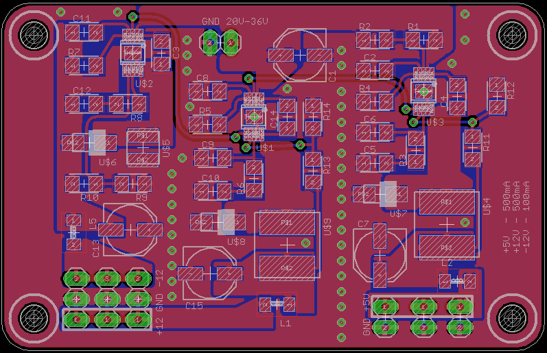
There has also been some work on the power supply for the bench supply, which requires +12V, -12V & +5V. I had looked at using a charge pump arrangement to give the -12V but when evaluating the current requirement it was not up to the job. So I have gone with a design from Texas Instruments for a 100mA -12V circuit using their TPS5401 part. [Ref. http://www.ti.com/tool/PMP7330]
Having switched to this it then made sense to use this as the basis for the +12V 500mA and +5V 500mA sections. When looking for the data sheet [Ref. http://www.ti.com/product/TPS5401] I discovered that Ti now have a pretty good online design tool; WEBBENCH Designer. Using this allowed me to quickly put together the circuits for the other two sections (the negative voltage version is not supported by WEBBENCH). The resulting design is below, circuit in the files section, still under consideration.
![]() I've made use of the cascaded startup that switches on the 5V section first and then the +12V and lastly the -12V. The board is designed to run three of the bench supply units at a time.
I've made use of the cascaded startup that switches on the 5V section first and then the +12V and lastly the -12V. The board is designed to run three of the bench supply units at a time. -
Design itterations
10/06/2016 at 01:04 • 0 commentsI've been playing with the design some more, and moved the large capacitor off the board. The linear control section was then relaid and separate grounds introduced for the analogue, digital and power sections.
Finally I've added a voltage difference section that maintains a constant 3v higher output of the switched section compared to the linear section using a difference amplifier than can be run off the max 36v input voltage.
The BOM cost is higher than expected, but the aim is for something that will last a few decades, board size is ~100x40mm.
![]()
![]()
-
First-pass design
09/30/2016 at 03:10 • 0 commentsAs mentioned in the heading, this is a positive section bench power supply based on Kerry Wong's supply. I've made some changes to suit 3A current and reduced the voltage control to match a 2.048V DAC and precision external reference for the ATMega328p which will handle control and display on I2C 16x2 LCD.
The +12V, -12V, +5V supply will be off the board and shared between up to three modules, I've yet to design this.
I've posted up TINA-TI simulation model of the linear section and the corresponding schematic for the module. Any comments welcomed.
![]()
OSH render of the rev A2 design