 Ted Yapo
I received the PCBs from OSH Park, maybe Friday I think, because I was away for a little while. I probably won't get to assemble one right away, but I did get a look at them. I especially wanted to see if my 4/5 design in a 6/6 process worked.
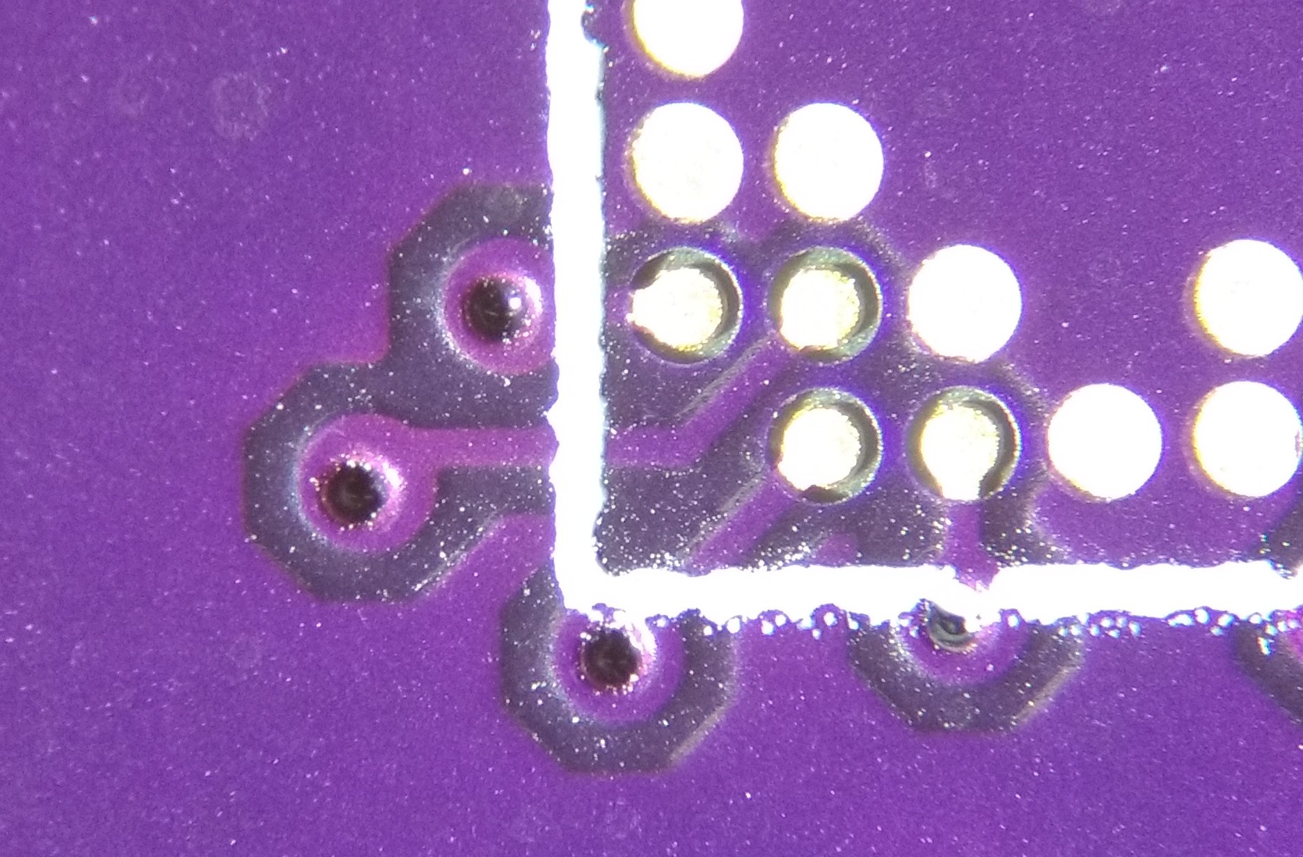
It looks like I got away with it on all three boards. I suspected I would - it's only a short trace. The thing that really struck me about this image, though, was how thick the soldermask is where the copper has been removed. At first glance, at least, it appears to be much thicker there than when it is over copper. I had somehow always imagined it as a uniform thickness over everything. Maybe it's actually supposed to fill-in the area where copper has been removed?
This fact has no bearing on the performance of the board, or the radar project in general, but I thought it was interesting.
Oh, and those 0.3mm BGA pad are small! As in, they are actually 0.3mm, which is the correct size.
Discussions
Become a Hackaday.io Member
Create an account to leave a comment. Already have an account? Log In.
Could you please email support@oshpark.com? We always appreciate feedback like this and will investigate. Thanks! -Drew Fustini
Are you sure? yes | no
Oh, I don't think there's a need for that: there's nothing wrong with the board, I just had never taken a very close look at the soldermask before, and found it interesting.
I have no doubt this is exactly like every other board I have ever ordered, and will work perfectly :-)
Are you sure? yes | no
I wonder if @oshpark could comment on this.
Are you sure? yes | no
I was hopping for some wisdom about the PCB making process.
Are you sure? yes | no
I am constantly hoping for wisdom. So far, none has been forthcoming ;-)
Are you sure? yes | no
Happy to! The precise answer is that the soldermask is a thin, translucent layer. As a result, the color of the mask is highly dependent on the material underneath it.
On any individual board, you have a pretty consistent thickness, making the main color driver what's below the mask. Copper is a light-ish color and reflective, so it winds up being a light color. The substrate is dark brown and nonreflective, so it winds up being really dark.
Thickness only really comes into play in odd cases. One of those is tented vias, in which case you often get thicker globs of mask. Another is that the color varies very slightly across manufacturing panels. You'll sometimes see this if you order and collect lots of boards.
Usually though, it's really difficult to properly assess color variation unless you're holding the board yourself. In photos, the lighting winds up having really gnarly effects. Low light levels make the boards look incredibly dark (even more so than would be expected), and the temperatue of the lighting will skew the color of the mask itself. Yellow makes the boards look brownish, and blue light makes them look really vivid. This is generally why the color looks so varied online.
Are you sure? yes | no
Thanks!
Are you sure? yes | no
I have also gotten away with 4 mil traces before, so I am glad this worked out on your design, but it is a tricky proposition. Via-in-pad is the standard way to do this but this increases the pcb cost by at least 10 fold, if not more. Not great for small prototyping.
In addition to the 27 gauge nozzle for the low temperature solder paste (if you go this route) I also use sharp tweezers (my main assembly tool) to corral errant solder paste back to where I want it (on the pads) when necessary. I have found that careful application of the solder paste (i.e., stay on the pads) is key, accurate placement is next in importance. I can routinely manage 0.4-mm pitch WLCSPs with 0.25-mm diameter pads (when via-in-pad can be avoided) using this method. I think your BGA package should be relatively straightforward after a bit of practice.
And the other nice thing about low temperature solder paste is if it doesnt work the first time, it is relatively easy to adjust the position of the component in case of misalignment (during heating) or remove the component, clean off the excess solder, and try again.
Are you sure? yes | no
I think you can easily buy stencils for the common BGA footprints.
Are you sure? yes | no