Ruud van Falier
-
Abandoning the project
09/08/2019 at 18:15 • 8 comments![]()
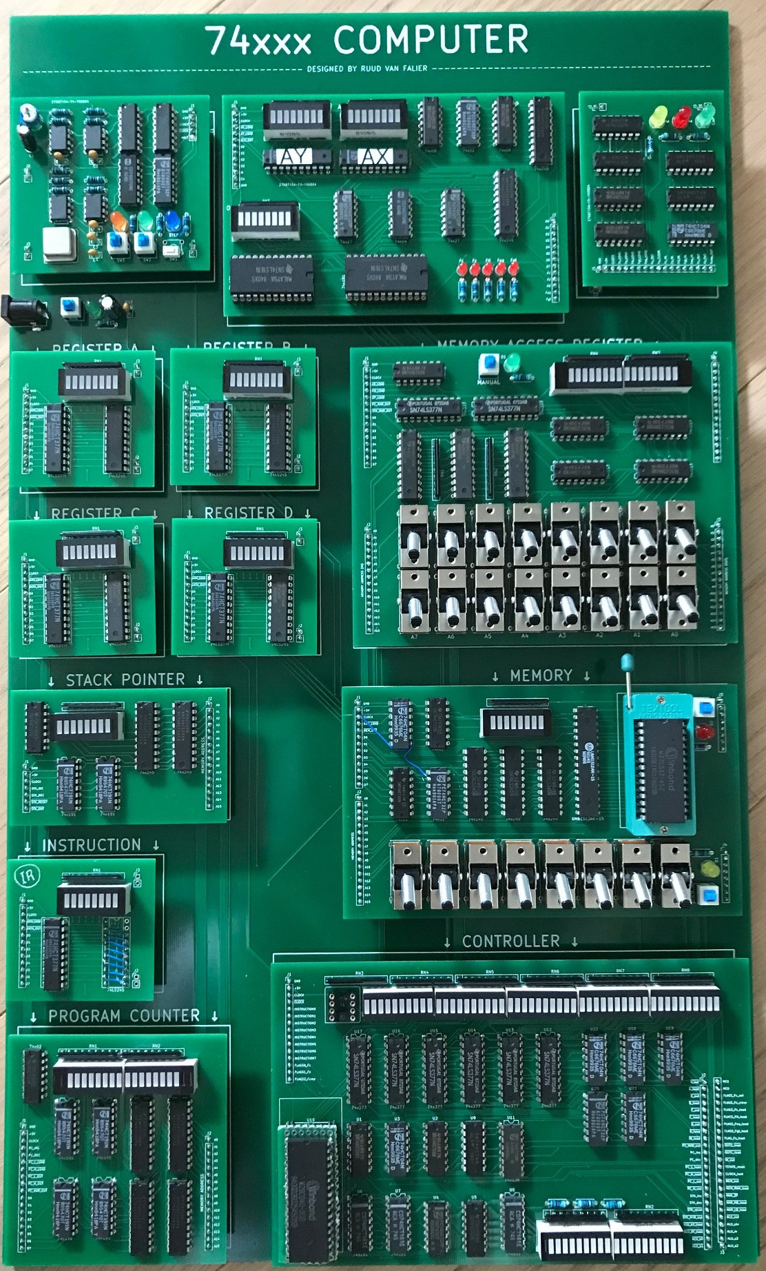
I got pretty far with this project; as far as actually getting everything built on PCB's.
Unfortunately I ran into some issues that prevent the real (non-simulated) computer from properly working:- I never considered reset circuitry:
- The 74x377 registers don't have a reset line, so the only way of resetting them is to load empty data.
- None of the modules have a reset line exposed
- I tried to "quick fix" this with a 2nd revision of the controller, but it failed
- The controller is way to complicated, which is a result of the way microcode is stored:
- Each instruction takes 6 bytes to store control lines state
- The controller has its own internal clock that runs independent from the rest
- In Logisim this results in a very slow simulation because every microtick (t-state) takes 6 clock cycles to retrieve control lines from the microcode ROM.
These issues don't necessarily mean I have to abandon the project - I could try to fix just those things and move on, but this project was done over the course of 1,5 years and I have learned a lot in that time!
I would prefer to apply all lessons learned to a completely new design.Even though the final product is not fully functional, I still consider this project to be a success. I've learned so much about (homebrew) CPU architecture, simulating designs in Logisim, assembly languages, digital electronics and much more.
And I'll take all that knowledge with me to the next project!The 74xx Computer Mk. II project will soon be shared here.
- I never considered reset circuitry:
-
PCB creation
07/26/2019 at 12:52 • 0 commentsAfter a bit of a pause I've picked up where I left.
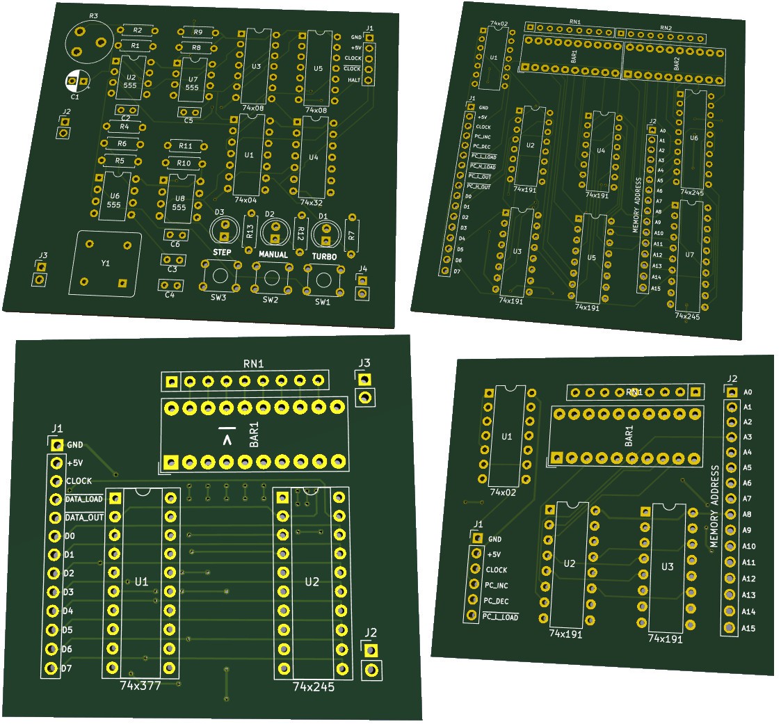
Now that the entire computer is working in Logisim, I've decided to try to bring it to life and solder the whole thing together.I'm going for a modular approach for which each of the computer's components (e.g. register, clock, stack pointer) is built as a separate PCB.
The inputs & outputs (control lines, address lines, data lines) for each module are exposed using male header pins. This allows me to easily test each module individually.
Once all the modules are in working order, they will be connected on each other on top of one large PCB with header sockets.At least that is the plan!
So far I've finished the Clock, Register(s), Progam Counter and Stack Point modules (although they are stil untested).
![]()
-
Assembly Language Reference
04/10/2019 at 09:14 • 3 commentsThe assembly language for the 74xx Computer has been finalized and documented: https://github.com/DutchMaker/TTL-computer/blob/master/Documentation/74xx-Assembly-Language.md
Everything that is mentioned in the reference is also implemented in the Logisim circuit, the microcode compiler and the assembler.
-
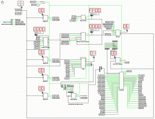
Hello World
04/08/2019 at 20:01 • 0 commentsThe entire instruction set has been implemented and the first Hello World program is running on the 74xx Computer in Logisim:
![]()
-
It's alive (in Logisim) !
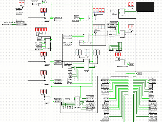
04/02/2019 at 15:03 • 1 commentThe control unit is done and the first bits of microcode have been created.
The computer is now running MVI, MOV and HALT instructions!![]()
-
Back after hibernation
03/26/2019 at 12:34 • 0 commentsIt's been a while, but the project is still alive! Lately I found the motivation to work on it again and the result is that the computer is now 95% finished in Logisim.
It has been good to see that everything that was in my head is actually working for real, at least in simulation. Hopefully that is enough to keep me going!
Status as of March 26th, 2019:
Work done in chronological order:
General architecture has been worked out as high level schematic (see: Architecture.pdf).
Needs to be updated according to Logisim design!Worked on instruction set, micro code, module documentation & general notes from time to time (see: Documentation). This is still heavily work in progress! I'm planning to write a short piece of documentation on each of the modules, like I did for the Sequencer / Instruction Decoder.
Needs to be updated according to Logisim design!Circuit diagrams have been worked out in KiCad for all modules except for the Sequence / Instruction Decoder (see: Schematics-KiCad). These circuits were designed in KiCad and not tested.
Needs to be updated according to Logisim design!The entire computer is being built in Logisim to verify all the circuits and the way I had everything in mind is actually going to work. I'd say it's 95% done as far as Logisim design goes, but it can't be fully tested until the entire instruction set and all microcode has been worked out.
While working on the Logisim design, I made several changes to the architecture and some to circuits. These changes still need to be applied to all previous work (architecture design, circuit diagrams, etc.)
TODO's / Plans:
- Rename the project to 74xx computer (it was named TTL Computer before, but it may technically not all be TTL).
- Updated previously made documentation according to latest Logisim design.
- Write new documentation on all modules
- Finish the computer in Logisim with the entire instruction set working.
- Build the computer in real life.
-
Updated architecture & instruction set
05/08/2018 at 11:49 • 0 commentsIn the past weeks I have prototyped small parts of the computer, thought things over and realized that I had to make a few adjustments to the architecture and instruction set.
Let me start with the progress that was made with the circuit diagrams. The following diagrams have been completed and some of them are tested:
- Clock [tested]
- Program counter
- A, B, C, D & Flags register [tested]
- ALU [partially tested in Logisim]
The following changes have been made to the architecture:
- The X & Y registers have been renamed to C & D, nothing shocking here.
- The ALU now has it's own internal accumulator register.
- Input for the ALU can now come from the A, C & D register (and not just fixed from the A register). The second operand still comes from B.
- Two outputs are now accounted for: decimal display (output 1) and serial (output 2)
The instruction set has a few new and updated instructions:MOV [A,B,X,Y] [A,B,X,Y] Copy register N2 to register N1 MVI [A,B,X,Y] #value Copy immediate value to register N LD [A,B,X,Y] $address Load register N with value at memory address ST [A,B,X,Y] $address Store register N value at memory address ADD [A, X, Y] N + B → N ADC [A, X, Y] N + B + 1 → N SUB [A, X, Y] N - B → N SBC [A, X, Y] N - B - 1 → N AND [A, X, Y] N & B → N OR [A, X, Y] N | B → N XOR [A, X, Y] N ⊕ B → N NOT [A, X, Y] !N → N INC [A, X, Y] N + 1 → N DEC [A, X, Y] N - 1 → N SHL [A, X, Y] Shift all bits in register N to the left SHR [A, X, Y] Shift all bits in register N to the right RAL [A, X, Y] Rotate all bits in register N to the left RAR [A, X, Y] Rotate all bits in register N to the right CMP [A, X, Y] Compare register N to register B JMP $address Jump to memory address JZ $address Jump to memory address if zero flag is set JNZ $address Jump to memory address if zero flag is not set JC $address Jump to memory address if carry flag is set JNC $address Jump to memory address if carry flag is not set JEQ $address Jump to memory address if N = B JLT $address Jump to memory address if N < B JGT $address Jump to memory address if N > B CALL $address Jump to subroutine at memory address RET Return from subroutine NOP Do nothing HLT Halt execution IN Load data from input into register A (needs to be worked out) OUT [1, 2] [A, B, X, Y] Output data from register N2 on output N1
(1 = decimal display, 2 = serial output)I'm currently waiting on more breadboards coming in for prototyping and slowly working out all the circuit diagrams in the meantime.
More updates coming soon!
-
Instruction set
04/29/2018 at 11:37 • 1 commentI've done a bit more work on defining the instruction set.
These are the instructions that I'm planning to implement and that should be supported by the architecture that has been worked out so far:MOV [A,B,X,Y] [A,B,X,Y] Copy register n1 to register n2 MVI [A,B,X,Y] #value Copy immediate value to register n LD [A,B,X,Y] $address Load register n with value at memory address ST [A,B,X,Y] $address Store register n value at memory address ADD A + B → A SUB A - B → A AND A & B → A OR A | B → A XOR A ⊕ B → A INC A + 1 → A DEC A - 1 → A RAL Rotate all bits in register A to the left RAR Rotate all bits in register A to the right JMP $address Jump to memory address JZ $address Jump to memory address if zero flag is set JNZ $address Jump to memory address if zero flag is not set JC $address Jump to memory address if carry flag is set JNC $address Jump to memory address if carry flag is not set CALL $address Jump to subroutine at memory address RET Return from subroutine NOP Do nothing HLT Halt execution IN Load data from input into register A (needs to be worked out) OUT Output data from register A (needs to be worked out) I haven't given much thought to input & output yet, so I might need a few specialized instructions in the future to cover that part.
-
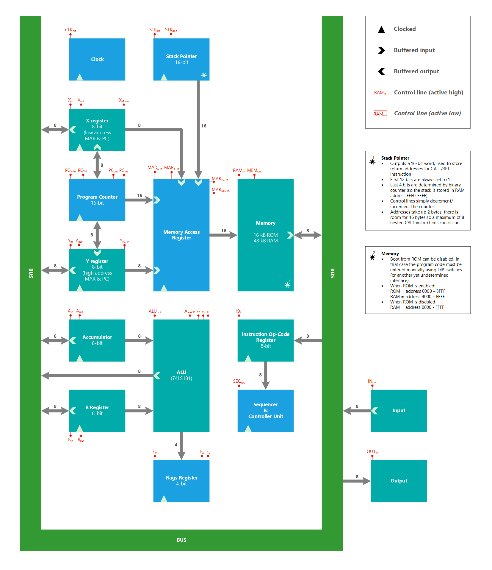
Architecture
04/27/2018 at 19:53 • 0 commentsMost of the computer's architecture has been worked out (at least on paper...)
Here is a schematic overview of the entire architecture:![]()
[View Architecture Overview] Let me explain what I have in mind:
- There is an 8-bit data bus and all the registers are 8-bit.
- 64 kB of memory can be accessed using a 16-bit address bus, managed by the memory access register.
- The memory consists of 16 kB ROM and 48 kB RAM.
- The program counter is 16-bit and can be loaded using the X and Y register.
The program counter output can be loaded into the memory access register. - The X and Y registers can also be used to load a 16-bit memory address directly into the memory access register.
- The A(ccumulator), B, X and Y registers can all be used to read and write to the data bus.
- I'm going with the 74181 for the ALU (which some will consider to be a shortcut).
- Input for the ALU comes from the Accumulator and B register, output is put on the data bus.
- The stack pointer is used while storing return addressed for CALL instructions. It's basically a 4-bit binary counter and the module outputs 16-bits in total of which the first 12-bits are always set to 1 and last 4 bits come from the counter. This means the stack is stored at FFF0-FFFF in RAM. Considering the fact that memory addresses take up 2 bytes, the stack allows for up to 8 nested subroutine calls.
- The ROM can be disabled. I want to be able to use this computer for educational purpose and have the option to manually put a program and RAM (using switches) instead of always booting from ROM.
- For the same educational purpose, but also for debugging purpose, the clock can run in several modes: single-step, slow variable mode (1 to 15 Hz) and turbo mode (1 MHz).
- Functionality for input and output modules still has to be determined.
- The computer will be driven by micro code. The instruction set is still under construction.
- Instructions consist of 1 to 3 bytes: 8-bit opcode and 16-bit data.
I really want to be able to use this machine to teach others about CPU architecture.
I'm planning to add LED indicators to all the modules in order to visualize the data flow.
Aside from that the machine can be single stepped and programs can be loaded straight into RAM using switches.
DM-01: 8-bit 74xx computer
Designing and building my own 8-bit computer from scratch with 74xx (TTL) logic chips