Second Pass Emulator
The second pass recoginises the I/O or ports are accessed via:
- REGA - the port address
- REGD - the port read/write
The third pass will add paged RAM and ROM.
Run out of room
Run out of room for the monitor, well I ran out of room a while ago when I "stubbed" the delay routine. Anyway I need to push some code onto ROM page 1 (i.e. the second page).
One of the monitor design "features" was to hide the ROM and RAM page registers from the front panel.
The problem is you cannot manually change the ROM page with monitor running.
The monitor should really have no reason to view the ROM code (on another ROM page) in any case.
Changing the RAM page would be okay, however. But the current design does not allow you to read the page registers and I have no pull ups (or pull down resistors on the Databus. So even changing RAM page is messy.
One way to read/write from/to a register and then copy that register to the RAM page at the end of the monitor rountine. Extra code is the cost for tis patch.
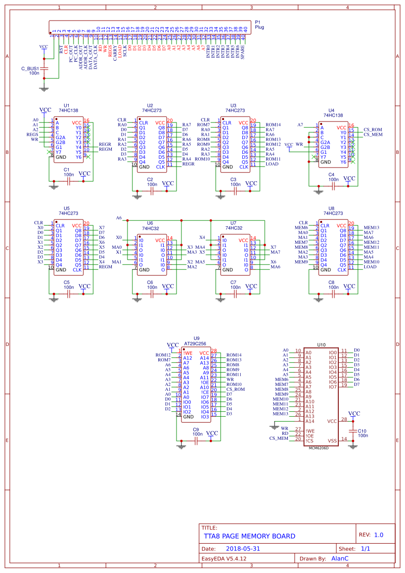
Checking the Page Memory Board schematic:

I need to add three chips (a decoder and two registers) for a total of 13 chips (crowded).
May be better to split the board into Page ROM and Page RAM.
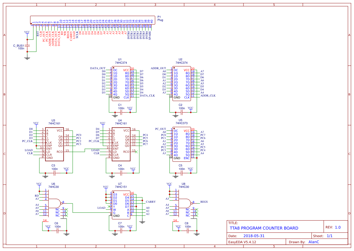
I should have added pull up resistors to the Program Counter Board:

It is no big deal, you should not be using the monitor to probe around in this area anyway as it will result in strange things happening as it may interfere with the monitor.
Progress
Anyway, the monitor code is progressing, but ever so slowly.
Version 3 will consider ROM/RAM paging (and require a significant code rework).
Okay I have a plan!
First what was the problem? Oh yeah, two paging systems and how to bring them together for the Interpreter.
Basically an "Instruction Address" has the format:
- Address
- Page
But the Page may be ROM or RAM or the static System area.
The answer is to look at the Address:
- 11XX XXXX System area (registers and static RAM)
- 10XX XXXX RAM Page
- 0XXX XXXX ROM Page
The code would look like this:
        POINTER ; Get the Address
        REGP
        _64     ; Test if 11xx xxxx (System area)
        REGQ
        _EXIT   ; Exit if System area
        JC
        _128    ; Text if 10xx xxxx (RAM Page area)
        REGQ
        _NEXT   ; Goto RAM Page
        JC
        PAGE    ; No, its ROM Page (0xxx xxxx)
        ROM
        _EXIT
        JMP
_NEXT:
        PAGE
        RAM
_EXIT:
So expensive for the Interpreter but what choice do I have? Without the issue of Page addressing the Interpret would look like this (5 machine instructions or 10 bytes):
INTERP    IP      ; SAVE IP
          POINTER
          IP      ; INC IP
          REGP
          _1
          REGQ
          ADD
          IP
          _246    ; ^POINTER
          JMP
With ROM Paging ONLY (no Address decoding) it would look like this (8 machine instructions):
INTERP    IP      ; SAVE IP
          POINTER
          IP      ; INC IP
          REGP
          _1
          REGQ
          ADD
          IP
          IP      ; GET ROM PAGE
          ROM
          IP      ; INC IP
          REGP
          ADD
          IP
          _246    ; ^POINTER
          JMP
With Address decoding (17 machine instructions):
INTERP    IP      ; SAVE IP
          POINTER
          IP      ; INC IP
          REGP
          _1
          REGQ
          ADD
          IP
          IP      ; GET ROM PAGE
          PAGE

;         PAGE ADDRESS DECODING
          POINTER ; GET ADDRESS
          REGP
          _64
          REGQ
          _EXIT   ; SYSTEM AREA
          JC
          _128
          REGQ
          _RAM    ; RAM PAGE
          JC
          PAGE    ; SET ROM PAGE
          ROM
          _EXIT
          JMP
_RAM      PAGE    ; SET RAM PAGE
          RAM
_EXIT     _1      ; RESTORE REGQ
          REGQ

; CONTINUE WITH INTERPRETER
         IP       ; INC IP
         REGP
         ADD
         IP
         _246     ; ^POINTER
         JMP
If you find the code above incomprehensible then you can understand why micro-coding is so slow and why an Interpreter is so important.
AlanX
 agp.cooper
Discussions
Become a Hackaday.io Member
Create an account to leave a comment. Already have an account? Log In.