-
Combining Projects
05/22/2018 at 01:59 • 0 comments![]()
With the experiments from the Digital Design Doohickey Project, which include a 555 timer system clock, a 4-bit binary counter for micro-program decoding, and a CPLD based I/O, along with the Mega-One-8-One ALU project, and the 4-bit architecture experiments done here, we can now begin a new project combining these projects together to create a robust modular 4-bit microprocessor system!
-
Test Me!
05/22/2018 at 01:38 • 0 comments![]()
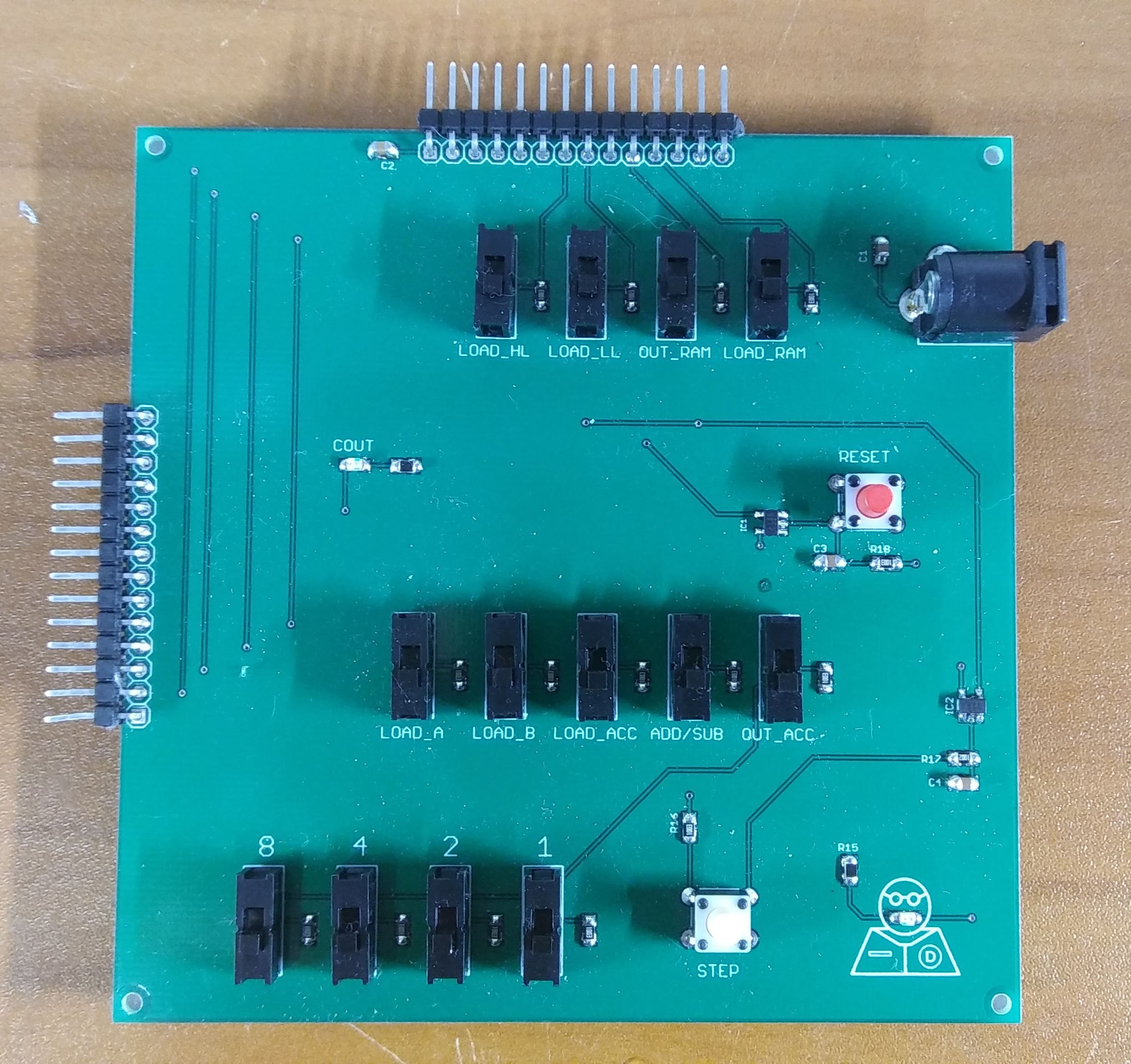
One of the most difficult aspects of microprocessors/microcontrollers is the decode and microprogramming features. To avoid dealing with these items at this stage in the experiments, I've created a test block that has Single-Pole Double-Throw (SPDT) slide switches that enable/disable each of the functions. I've also added in a reset button, and a "STEP" button that produces a "clock" which would be generated by the system clock in a real system. In addition, I've added 4 switches that allow me to enter data directly to the main 4-bit data bus. The barrel jack provides +5V regulated input to the system.
-
I'm Registered!
05/22/2018 at 01:25 • 0 comments![]()
The ALU section of the design contains a 4-bit register A (74HC173D), and a 4-bit register B(74HC173D). These are individually addressable but the main 4-bit data bus, and provide output only to the "ALU". The ALU section consists of a 4-bit full adder 74HC283D, and is supplemented with a quad XOR from register B, which enables 4-bit subtraction. The ALU output is latched into a separate 4-bit register labeled as the Accumulator, which has an selectable output to the main 4-bit databus. This design was directly inspired by the SAP-1 (Simple as Possible) attributed to Paul Malvino (not Ben Eater as some would believe). As a debug item, I've added LEDs on the main data bus to indicate what is being presented on the bus at any given cycle...
-
Thanks for the Memory
05/22/2018 at 00:59 • 0 comments![]()
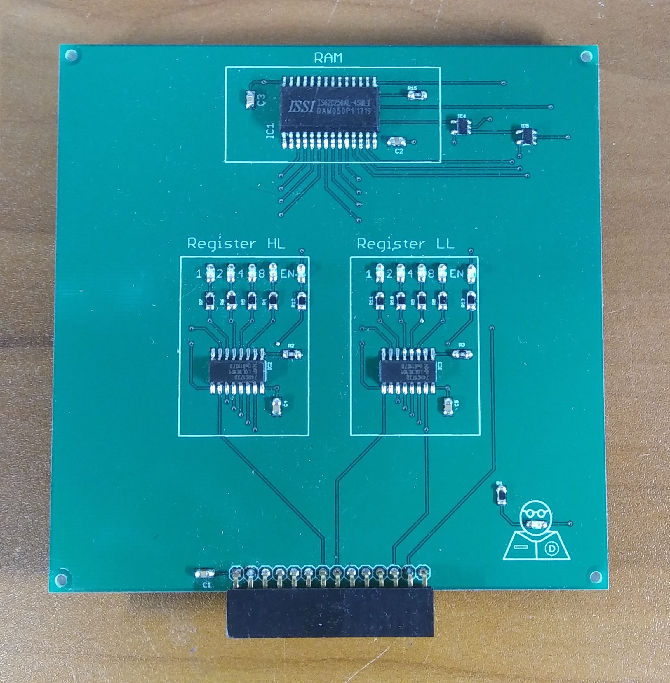
One of the fundamental items for a microprocessor/microcontroller system is the ability to have read/write memory storage. After carefully reading many of the datasheets for original 4-bit systems, it was apparently that many used either a latch or register to control the memory address access to the memory. In my design I've used two 74HC173D which are 4-bit wide. One is used for the upper 4-bits of the memory address, and another for the lower 4-bits. The memory itself is a 32K x 8 parallel SRAM chip (IS62C256AL). This simple module is the basis of the read/write memory for these experiments.
4-Bit Architecture Experiments
Modular experiment around a 4-bit processor architecture
 Dave's Dev Lab


