-
Output Instruction
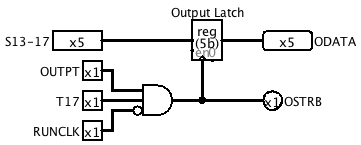
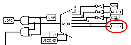
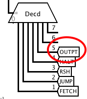
11/18/2018 at 01:07 • 0 commentsThe Output instruction takes the upper 5 bits of a memory word and sends it to an alphanumeric output device, originally a teleprinter. I'm not sure exactly what kind of output device I'm going to use yet, so at this stage I've just designed a rudimentary parallel output interface with a strobe output OSTRB and a busy input OBSY. It consists of a 5-bit transparent latch fed from outputs 13 to 15 of the S register, and gating to load it and generate the strobe pulse during T17 when MISC = OUTPT. The OBSY input is connected to the microcode branch multiplexer.
I used a transparent latch instead of an edge-triggered one because I want the outputs to be valid before the trailing edge of the strobe. I found it necessary to gate the strobe with the second half of the bit clock cycle, to ensure that its trailing edge occurs while the inputs to the latch are still valid.
![]()
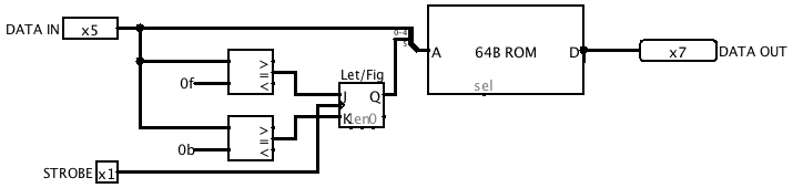
For testing purposes, I also mocked up an emulation of a 5-bit teleprinter using a Logisim TTY component, a ROM to translate from EDSAC character codes to ASCII, and a flip-flop to keep track of the letters/figures shift state.![]()
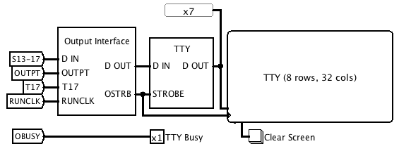
This is how it all fits together on the main circuit.![]()
![]()
![]()
![]()
And here's the microcode. It loops until OBSY is not active, and then reads from memory into the S-register and loads the output latch.OUTPT = 101 # Load output register and send output strobe BOBSY = 101 # Output device busy # O - Output 01001 0 0001 : - - -- --- - -- -- -- - - - - - - - --- - BOBSY 1000 # Loop until output device ready 01001 0 0010 : SHS EOI -- --- - -- -- -- - - - - - - - OUTPT - --- ---- # Read memory and perform output
-
A Well-Rounded Instruction
11/16/2018 at 05:21 • 0 commentsThe Round instruction is meant to round the accumulator to 34 fractional bits, by adding 1 at bit 36 if bit 35 is 1. I managed to implement this without making any changes to the hardware. The strategy is to first shift word 1 of the accumulator left by one bit (by adding it to itself), so that bit 35 ends up in the carry flag, and then add the carry to words 2 and 3. Finally, words 0 and 1 are cleared.
# Y - Round accumulator to 34 fractional bits
   00110 0 0001 :  -   -   10  XAC   -  YAC   CY0  --   -   -   -  LSW  -    -    -   ---     -   ---    ----    # Shift word 1 of AC left
   00110 0 0010 :  -   -   01  XAC   -  Y0    --   WAC  -   -   -   -   -    -    -   ---     -   ---    ----    # Add carry to AC words 2 and 3
   00110 0 0011 :  -   -   11  XAC   -  Y0    --   WAC  -   -  MSW  -   -    -    -   ---     -   ---    ----
   00110 0 0100 :  -   -   00  X0    0  Y0    CY0  WAC  -   -   -  LSW  -    -    -   ---     -   ---    ----    # Clear AC words 0 and 1
   00110 0 0101 :  -  EOI  10  X0    0  Y0    --   WAC  -   -   -   -   -    -    -   ---     -   ---    ----
-
Jump Instructions, and correcting an error
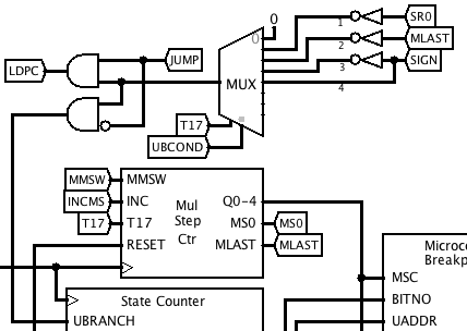
11/15/2018 at 10:10 • 0 commentsThe original EDSAC had two conditional jump instructions (and no unconditional one!), namely Jump if Accumulator >= 0 and Jump if Accumulator < 0. For implementing these, I added a new MISC value called JUMP and two new UBCOND values for testing the SIGN output of the ALU, called BSGN0 and BSGN1.
However, I didn't want to actually use these to perform microcode branching, because then a jump instruction would require up to two cycles, one to test the sign bit and one to load the PC if the test is true. To save a cycle, I arranged things so that JUMP suppresses microcode branching and instead activates a new signal LDPC during T17 if the microcode branch condition is true. This allows the jump to occur at the end of the same cycle that tests the sign.
The microcode branch condition circuitry now looks like this:
![]() LDPC causes the program counter to be loaded from the address field of the instruction register:
LDPC causes the program counter to be loaded from the address field of the instruction register:
![]() Here is the microcode for the jump instructions. Each one consists of just a single microinstruction that passes the accumulator through the ALU and activates JUMP together with the appropriate condition.
Here is the microcode for the jump instructions. Each one consists of just a single microinstruction that passes the accumulator through the ALU and activates JUMP together with the appropriate condition.JUMP = 010 # Conditionally load PC from address field of instruction BSGN0 = 110 # Sign FF = 0 BSGN1 = 001 # Sign FF = 1 # E - Jump if accumulator >= 0 00011 0 0001 : - EOI 11 XAC - Y0 CY0 -- - - MSW LSW - - - JUMP - BSGN0 ---- # G - Jump if accumulator < 0 11011 0 0001 : - EOI 11 XAC - Y0 CY0 -- - - MSW LSW - - - JUMP - BSGN1 ----
Update to Transfer and Clear instructions
While doing some more research into the EDSAC, I realised that my implementations of the Transfer and Clear instructions weren't quite right -- they were only clearing the parts of the accumulator that were being written to memory, whereas they are supposed to clear the whole accumulator. I've fixed them, but it means they now take 4 cycles to execute. This is annoying, but there doesn't seem to be anything I can easily do about it.
# T - Transfer and clear
   00101 0 0001 :  -   -   00  XAC  CMX YAC   CY1  WAC  -   -   -  LSW  -    -    -   ---     -   ---    ----
   00101 0 0010 :  -   -   10  XAC  CMX YAC   --   WAC  -   -   -   -   -    -    -   ---     -   ---    ----
   00101 0 0011 :  -   -   01  XAC  CMX YAC   --   WAC  -   -   -   -   -    -    -   ---     -   ---    ----
   00101 0 0100 :  -  EOI  11  XAC  CMX YAC   --   WAC  -   -  MSW  -   -    -   WMEM ---     -   ---    ----

   00101 1 0001 :  -   -   00  XAC  CMX YAC   CY1  WAC  -   -   -  LSW  -    -    -   ---     -   ---    ----
   00101 1 0010 :  -   -   10  XAC  CMX YAC   --   WAC  -   -   -   -   -    -    -   ---     -   ---    ----
   00101 1 0011 :  -   -   01  XAC  CMX YAC   --   WAC EVN  -   -   -   -    -   WMEM ---     -   ---    ----
   00101 1 0100 :  -  EOI  11  XAC  CMX YAC   --   WAC ODD  -  MSW  -   -    -   WMEM ---     -   ---    ----
-
Multiply Instructions
11/14/2018 at 07:19 • 0 commentsMicrocode for the single-word Multiply and Add instruction:
# OPCODE L STAT : SHS EOI  RFA XSEL CMX YSEL CARRY WRF ODD SS1 MSW LSW MMSW MLSW WMEM MISC  INCMS UBCOND UBADDR

# V - Multiply and add
   11111 0 0001 : SHS  -   00  X0    -  Y0    CY0  --   -   -   -   -   -    -    -   ---     -    ---    ----    # Read multiplier into S
   11111 0 0010 :  -   -   01  X0    -  YPR   CY0  WPR  -   -   -  LSW MMSW MLSW  -   RSH     -    ---    ----    # Multiply step word 2
   11111 0 0011 :  -   -   11  XMUL  -  YPR   CY0  WPR  -  SS1 MSW  -  MMSW MLSW  -   RSH   INCMS  010    0100    # Multiply step word 3
   11111 0 0100 :  -   -   01  XAC   -  YPR   CY0  WAC  -   -   -  LSW  -    -    -   ---     -    ---    ----    # Add product to AC word 2
   11111 0 0101 :  -  EOI  11  XAC   -  YPR   CY0  WAC  -   -  MSW  -   -    -    -   ---     -    ---    ----    # Add product to AC word 3
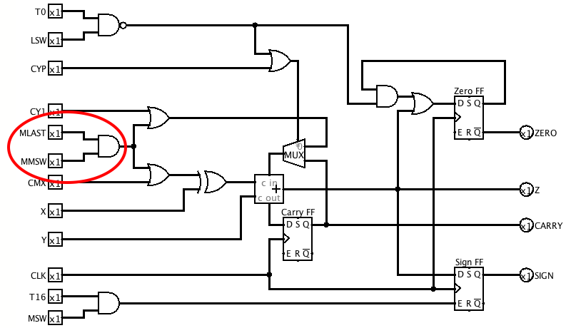
When I came to do the double-word version, I discovered an error in the ALU. It was treating bit 17 of the low word of the multiplicand as a sign bit and triggering subtraction. The following ALU update fixes this by gating MLAST with MMSW.
![]()
The microcode for double-word Multiply and Add consists of two four-cycle loops, one for each half of the multiplicand, followed by a final four cycles to add the Product Register to the Accumulator.11111 1 0001 : SHS - 00 --- - -- -- -- EVN - - - - - - --- - --- ---- # Read LSW of multiplier into S 11111 1 0010 : - - 00 X0 - YPR CY0 WPR - - - LSW - MLSW - RSH - --- ---- # Multiply step word 0 11111 1 0011 : - - 10 X0 - YPR -- WPR - - - - - MLSW - RSH - --- ---- # Multiply step word 1 11111 1 0100 : - - 01 XMUL - YPR -- WPR - - - - - MLSW - RSH - --- ---- # Multiply step word 2 11111 1 0101 : - - 11 XMUL - YPR -- WPR - SS1 MSW - - MLSW - RSH INCMS BNLMS 0100 # Multiply step word 3 11111 1 0110 : SHS - 00 --- - -- -- -- ODD - - - - - - --- - --- ---- # Read MSW of multiplier into S 11111 1 0111 : - - 00 X0 - YPR CY0 WPR - - - LSW MMSW - - RSH - --- ---- # Multiply step word 0 11111 1 1000 : - - 10 X0 - YPR -- WPR - - - - MMSW - - RSH - --- ---- # Multiply step word 1 11111 1 1001 : - - 01 XMUL - YPR -- WPR - - - - MMSW - - RSH - --- ---- # Multiply step word 2 11111 1 1010 : - - 11 XMUL - YPR -- WPR - SS1 MSW - MMSW - - RSH INCMS BNLMS 1110 # Multiply step word 3 11111 1 1011 : - - 00 XAC - YPR CY0 WAC - - - LSW - - - --- - --- ---- # Add product to AC word 0 11111 1 1100 : - - 10 XAC - YPR -- WAC - - - - - - - --- - --- ---- # Add product to AC word 1 11111 1 1101 : - - 01 XAC - YPR -- WAC - - - - - - - --- - --- ---- # Add product to AC word 2 11111 1 1110 : - EOI 11 XAC - YPR -- WAC - - MSW - - - - --- - --- ---- # Add product to AC word 3
The Multiply and Subtract instructions are identical except for subtracting the product from the accumulator.
# N - Multiply and subtract
   10110 0 0001 : SHS  -   --  ---   -  --    --   --   -   -   -   -   -    -    -   ---     -   ---    ----    # Read multiplier into S
   10110 0 0010 :  -   -   01  X0    -  YPR   CY0  WPR  -   -   -  LSW MMSW MLSW  -   RSH     -   ---    ----    # Multiply step word 2
   10110 0 0011 :  -   -   11  XMUL  -  YPR   --   WPR  -  SS1 MSW  -  MMSW MLSW  -   RSH   INCMS BNLMS  0100    # Multiply step word 3
   10110 0 0100 :  -   -   01  XPR  CMX YAC   CY1  WAC  -   -   -  LSW  -    -    -   ---     -   ---    ----    # Subtract product from AC word 2
   10110 0 0101 :  -  EOI  11  XPR  CMX YAC   --   WAC  -   -  MSW  -   -    -    -   ---     -   ---    ----    # Subtract product from AC word 3

   10110 1 0001 : SHS  -   00  ---   -  --    --   --  EVN  -   -   -   -    -    -   ---     -   ---    ----    # Read LSW of multiplier into S
   10110 1 0010 :  -   -   00  X0    -  YPR   CY0  WPR  -   -   -  LSW  -   MLSW  -   RSH     -   ---    ----    # Multiply step word 0
   10110 1 0011 :  -   -   10  X0    -  YPR   --   WPR  -   -   -   -   -   MLSW  -   RSH     -   ---    ----    # Multiply step word 1
   10110 1 0100 :  -   -   01  XMUL  -  YPR   --   WPR  -   -   -   -   -   MLSW  -   RSH     -   ---    ----    # Multiply step word 2
   10110 1 0101 :  -   -   11  XMUL  -  YPR   --   WPR  -  SS1 MSW  -   -   MLSW  -   RSH   INCMS BNLMS  0100    # Multiply step word 3
   10110 1 0110 : SHS  -   00  ---   -  --    --   --  ODD  -   -   -   -    -    -   ---     -   ---    ----    # Read MSW of multiplier into S
   10110 1 0111 :  -   -   00  X0    -  YPR   CY0  WPR  -   -   -  LSW MMSW  -    -   RSH     -   ---    ----    # Multiply step word 0
   10110 1 1000 :  -   -   10  X0    -  YPR   --   WPR  -   -   -   -  MMSW  -    -   RSH     -   ---    ----    # Multiply step word 1
   10110 1 1001 :  -   -   01  XMUL  -  YPR   --   WPR  -   -   -   -  MMSW  -    -   RSH     -   ---    ----    # Multiply step word 2
   10110 1 1010 :  -   -   11  XMUL  -  YPR   --   WPR  -  SS1 MSW  -  MMSW  -    -   RSH   INCMS BNLMS  1110    # Multiply step word 3
   10110 1 1011 :  -   -   00  XPR  CMX YAC   CY0  WAC  -   -   -  LSW  -    -    -   ---     -   ---    ----    # Subtract product from AC word 0
   10110 1 1100 :  -   -   10  XPR  CMX YAC   --   WAC  -   -   -   -   -    -    -   ---     -   ---    ----    # Subtract product from AC word 1
   10110 1 1101 :  -   -   01  XPR  CMX YAC   --   WAC  -   -   -   -   -    -    -   ---     -   ---    ----    # Subtract product from AC word 2
   10110 1 1110 :  -  EOI  11  XPR  CMX YAC   --   WAC  -   -  MSW  -   -    -    -   ---     -   ---    ----    # Subtract product from AC word 3
-
Improving the Microassembler
11/11/2018 at 04:53 • 3 commentsIn an effort to make the microcode source more readable, I added the ability to define named constants to the microassembler. They can be referenced anywhere in the source file, and they simply get textually expanded into their definitions.
This is what the microcode looks like now. While still not exactly crystal clear to the uninitiated, I hope you'll agree it's better than it was.AddressBits := 10 DataBits := 32 # Unused field values - = 0 -- = 00 --- = 000 ---- = 0000 # Single bit values SHS = 1 # Shift S Register EOI = 1 # End of Instruction CMX = 1 # Complement X ODD = 1 # MSW of double word memory reference MSW = 1 # Most significant word LSW = 1 # Least significant word SS1 = 1 # Shift S Register by one bit WMEM = 1 # Write memory INCMS = 1 # Increment multiplication step counter MMSW = 1 # MSW of multiplicand MLSW = 1 # LSW of multiplicand # WRF values WAC = 10 # Write Accumulator WMR = 01 # Write Multiplier Register WPR = 11 # Write Product Register # XSEL values X0 = --- # Zero XAC = 100 # Accumulator XMEM = 010 # Memory XMUL = 110 # S Register * Nultiplier XPR = 001 # Product Register # YSEL values Y0 = 00 # Zero YAC = 10 # Accumulator YAND = 01 # Multiplier & Memory YPR = 11 # Product Register, or zero if first multiplication step # Carry control values (CY1, CYP) CY0 = 00 CY1 = 10 CYP = 01 # MISC values FETCH = 100 # Instruction fetch RSH = 110 # Right shift HALT = 001 # Halt at end of instruction # OPCODE L STAT : SHS EOI RFA XSEL CMX YSEL CARRY WRF ODD SS1 MSW LSW MMSW MLSW WMEM MISC INCMS UBCOND UBADDR # Fetch xxxxx x 0000 : SHS - -- --- - -- -- -- - - - - - - - FETCH - --- ---- # A - Add 11100 0 0001 : - EOI 11 XMEM - YAC CY0 WAC - - MSW LSW - - - --- - --- ---- 11100 1 0001 : - - 01 XMEM - YAC CY0 WAC - - - LSW - - - --- - --- ---- 11100 1 0010 : - EOI 11 XMEM - YAC CYP WAC ODD - MSW - - - - --- - --- ---- # S - Subtract 01100 0 0001 : - EOI 11 XMEM CMX YAC CY1 WAC - - MSW LSW - - - --- - --- ---- 01100 1 0001 : - - 01 XMEM CMX YAC CY1 WAC - - - LSW - - - --- - --- ---- 01100 1 0010 : - EOI 11 XMEM CMX YAC CYP WAC ODD - MSW - - - - --- - --- ---- # Z - Halt 01101 0 0001 : - EOI -- --- - -- -- -- - - - - - - - HALT - --- ---- # T - Transfer and clear 00101 0 0001 : - EOI 11 XAC CMX YAC CY1 WAC - - MSW LSW - - WMEM --- - --- ---- 00101 1 0001 : - - 01 XAC CMX YAC CY1 WAC - - - LSW - - WMEM --- - --- ---- 00101 1 0010 : - EOI 11 XAC CMX YAC CYP WAC ODD - MSW - - - WMEM --- - --- ---- # U - Transfer without clear 00111 0 0001 : - EOI 11 XAC - Y0 CY0 -- - - - - - - WMEM --- - --- ---- 00111 1 0001 : - - 01 XAC - Y0 CY0 -- - - - - - - WMEM 00111 1 0010 : - EOI 11 XAC - Y0 CY0 -- ODD - - - - - WMEM --- - --- ---- # H - Load Multiplier 10101 0 0001 : - - 01 X0 - Y0 CY0 WMR - - - LSW - - - --- - --- ---- 10101 0 0010 : - EOI 11 XMEM - Y0 CY0 WMR - - MSW - - - - --- - --- ---- 10101 1 0001 : - - 01 XMEM - Y0 CY0 WMR - - - LSW - - - --- - --- ---- 10101 1 0010 : - EOI 11 XMEM - Y0 CY0 WMR ODD - MSW - - - - --- - --- ---- # C - Collate 11110 0 0001 : - EOI 11 XAC - YAND CY0 WAC - - MSW LSW - - - --- - --- ---- 11110 1 0001 : - - 01 XAC - YAND CY0 WAC - - - LSW - - - --- - --- ---- 11110 1 0010 : - EOI 11 XAC - YAND CY0 WAC ODD - MSW - - - - --- - --- ---- # L - Left shift 11001 x 0001 : - - 00 XAC - YAC CY0 WAC - - - LSW - - - --- - --- ---- 11001 x 0010 : - - 10 XAC - YAC CY0 WAC - - - - - - - --- - --- ---- 11001 x 0011 : - - 01 XAC - YAC CY0 WAC - - - - - - - --- - --- ---- 11001 x 0100 : - EOI 11 XAC - YAC CY0 WAC - SS1 MSW - - - - --- - 100 1000 # R - Right shift 00100 x 0001 : - - 00 XAC - Y0 CY0 WAC - - - LSW - - - RSH - --- ---- 00100 x 0010 : - - 10 XAC - Y0 CY0 WAC - - - - - - - RSH - --- ---- 00100 x 0011 : - - 01 XAC - Y0 CY0 WAC - - - - - - - RSH - --- ---- 00100 x 0100 : - EOI 11 XAC - Y0 CY0 WAC - SS1 MSW - - - - RSH - 100 1000
-
Fixing the Multiplication Algorithm
11/11/2018 at 03:03 • 1 commentWhen I tried to implement the multiplication scheme I described earlier, I found that it didn't work properly. It turns out my assumption that shifting the product right would be equivalent to shifting the multiplier left is not quite true.
To see the problem, let's do this example again using the product-shifting technique:0.75 * 0.6875 = 0.515625
The initial S-register and Multiplier values are:
                  17 16 15 14 13 12
S Register:        0. 1  1  0  0  0  ...
Multiplier:        0. 1  0  1  1  0  ...
The product register is zero until multiplication step 15, where the multiplier is added to it for the first time.
Product:           0. 0  0  0  0  0  ...
Multiplier:        0. 1  0  1  1  0  ...
                   ---------------------
New Product:       0. 1  0  1  1  0  ...
The product is then shifted right and the multiplier is added to it again.
Shifted Product:   0. 0  1  0  1  1  0  ...
Multiplier:        0. 1  0  1  1  0  0  ...
                   ------------------------
New Product:       1. 0  0  0  0  1  0  ...
Note that the sign bit of the product is now 1. However, the product is not negative -- it can't be, since it was obtained by adding two positive numbers! If we continue and perform the final step of the multiplication, the product register is shifted right again with sign extension and we obtain a negative result, which is incorrect.
Final Product: 1. 1 0 0 0 0 1 0 ... Wrong
In essence, the problem is that the product register overflows. To avoid this, we need an extra bit of precision on the left, between the binary point and the sign bit. Here's how that looks:
                  17 16 15 14 13 12 11
S Register:        0  0. 1  1  0  0  0  ...
Multiplier:        0  0. 1  0  1  1  0  ...

Product:           0  0. 0  0  0  0  0  ...
Multiplier:        0  0. 1  0  1  1  0  ...
                   ------------------------
New Product:       0  0. 1  0  1  1  0  ...

Shifted Product:   0  0. 0  1  0  1  1  0  ...
Multiplier:        0  0. 1  0  1  1  0  0  ...
                   ---------------------------
New Product:       0  1. 0  0  0  0  1  0  ...

Final Product:     0  0. 1  0  0  0  0  1  0  ...
Moving the Unused Bit (Again)
To provide the required extra bit of precision in the product register, I've decided to move the unused bit back to the most significant end. The reason I moved it before -- to get the final product aligned correctly -- turns out not to be a problem as long as multiplication is stopped once the sign bit (now the next-most-significant bit) of the multiplicand (in the S-register) has been processed.
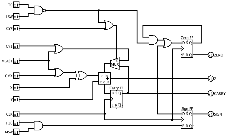
So I have undone most of the modifications I made earlier to put the unused bit at the least significant end. However, the ALU treats it as an ordinary bit -- I am not forcing it to be equal to the sign bit as I did before. That shouldn't be necessary, since they will end up equal anyway unless an overflow occurs, and I may want to implement overflow detection later by comparing them.Revised ALU
In the process of updating the ALU I discovered some other mistakes that were no doubt contributing to my messed-up multiplication results. This is the new ALU subcircuit.
![]()
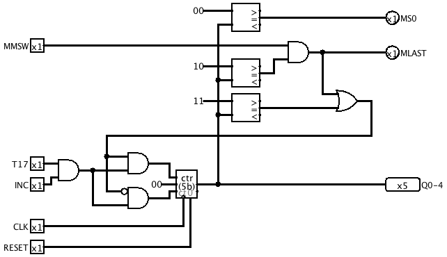
Revised Multiplication Step Counter
The MSC subcircuit now signals MLAST (last multiplication step) and wraps to zero on T16 of MMSW (most significant word of multiplicand). On the least significant word of the multiplicand, it wraps on T17.
![]()
Changes to Microcode Encoding
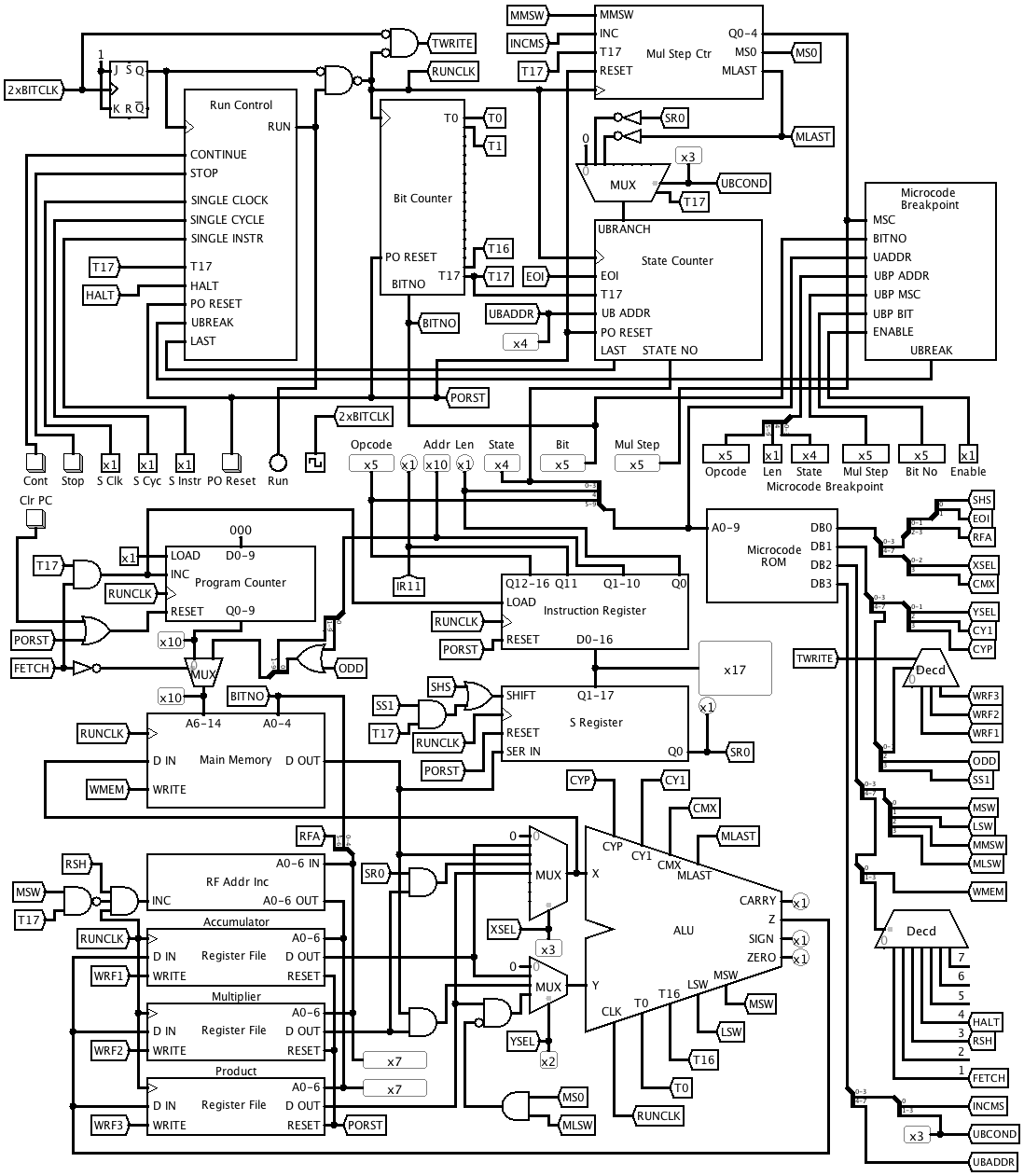
I discovered that encoding MMSW and MLSW as values of the MISC field wasn't going to work, because I need them both at once during a single word multiplication. I could have used yet another MISC value to represent the combination, but I realised a couple of things. I don't really need the MASEL field, because it's only ever used during an instruction fetch, and FETCH is never used together with any other MISC values. So I decided to allocate a MISC value for FETCH, and use it to control both memory address selection and PC incrementing, freeing up two microcode bits to use for MMSW and MLSW. This also simplified some of the other logic a bit, because MMSW and MLSW no longer need to imply RSH.
I also shuffled some of the microcode bits around, resulting in the following version of the main circuit.
![]()
-
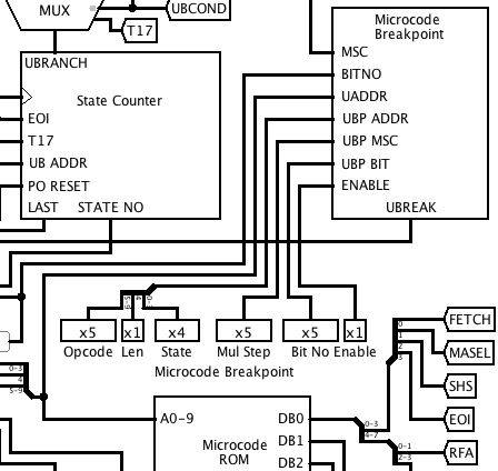
Microcode Breakpoints
10/26/2018 at 12:10 • 0 commentsWhile debugging my multiplication instructions, I decided that I needed a way to set a breakpoint in the microcode. I added some manually-controlled inputs to specify the microcode address, multiplication step count and bit number to break at, and a breakpoint enable signal. To make the wiring a bit tidier in the main circuit, I also grouped all the microcode address lines into a bus.
![]()
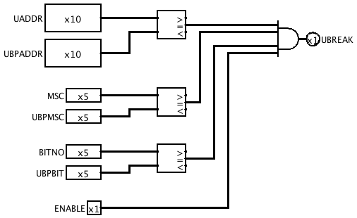
The Microcode Breakpoint subcircuit compares the current values of the microcode address, multiplication step and bit number with the breakpoint values. When they match, and breakpoints are enabled, the UBREAK output is activated.
![]()
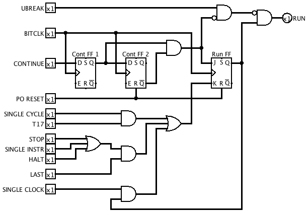
UBREAK is connected to the Run Control subcircuit, where it disables the RUN output, freezing the rest of the machine. To allow continuing after a break, I made some other changes to the run control circuit. When the CONTINUE button is pressed, a pulse lasting a single clock cycle is generated by Cont FF 1 and Cont FF 2. This pulse temporarily overrides the UBREAK input and allows a BITCLK cycle through. Since this advances the bit counter, the break condition will no longer be met in the next cycle, so execution continues until the breakpoint is reached again or the nachine is stopped by other means.
The Stop FF is no longer needed and has been removed. The Run FF is now set directly by the Continue pulse.
![]()
-
Multiplication Hardware
10/26/2018 at 12:02 • 0 commentsMoving the Unused Bit
Here are the changes I made to move the unused bit to the least significant end.
- The carry-in logic and initialisation of the Zero FF now takes place at T1 of an LSW instead of T0.
- The logic for extending bit 16 to bit 17 of an MSW has been removed, and the sign is captured in the Sign FF during T17 instead of T16.
- The Z ouput of the ALU is now forced to zero during T0 of an LSW.
- Inputs to the Instruction Register are taken from outputs Q2-18 of the S Register (where Q18 is the same as the serial input).
- Shift Left and Shift Right instructions are now terminated when bit 1 of the S Register is 1 instead of bit 0.
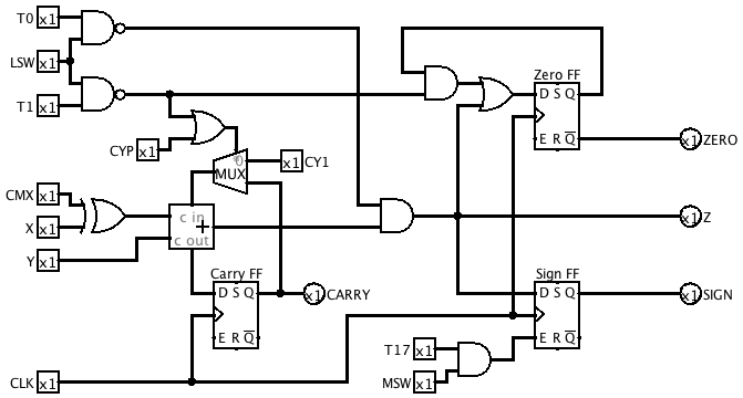
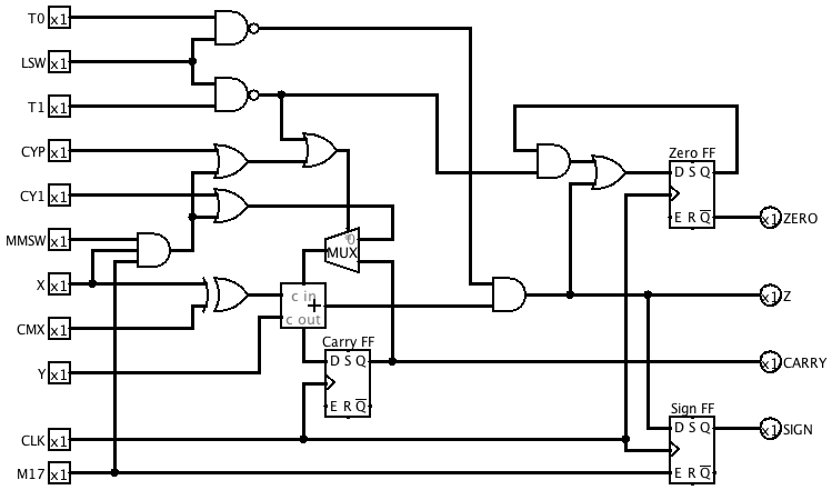
This is the revised ALU subcircuit:
![]()
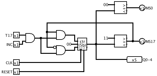
Multiplication Step Counter
We need a way to tell when we've carried out the required number of shift-and-add cycles when multiplying. The Multiplication Step Counter (MSC) does this. It counts up to 17 and then wraps back to 0 ready for another multiplication. A new control signal INCMS enables incrementing the MSC, and a new microcode branch condition (number 2) tests whether the MSC has reached 17.
![]()
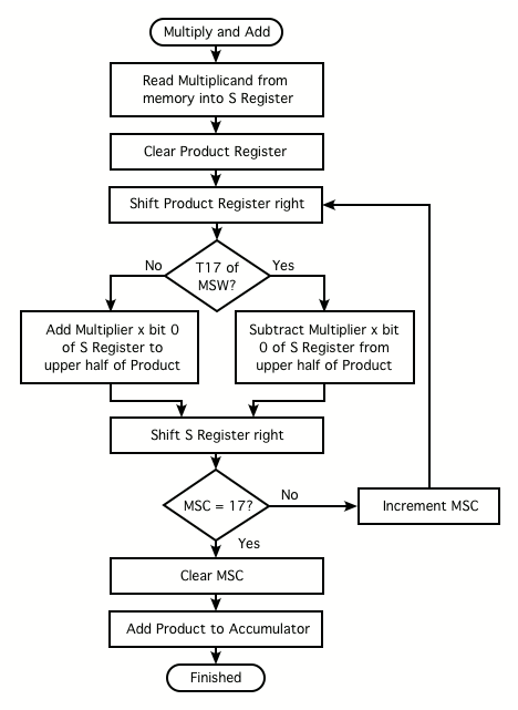
Multiplication Flowchart
Here's a flowchart showing the general strategy for implementing the Multiply and Add (V) instruction.
![]()
We can combine some of the operations that are shown as separate steps in the above flowchart. Not only will this save time, it will be necesessary if we want to stay within our 15-microinstruction budget for the long-word versions of the multiplication instructions.Other changes to support multiplication
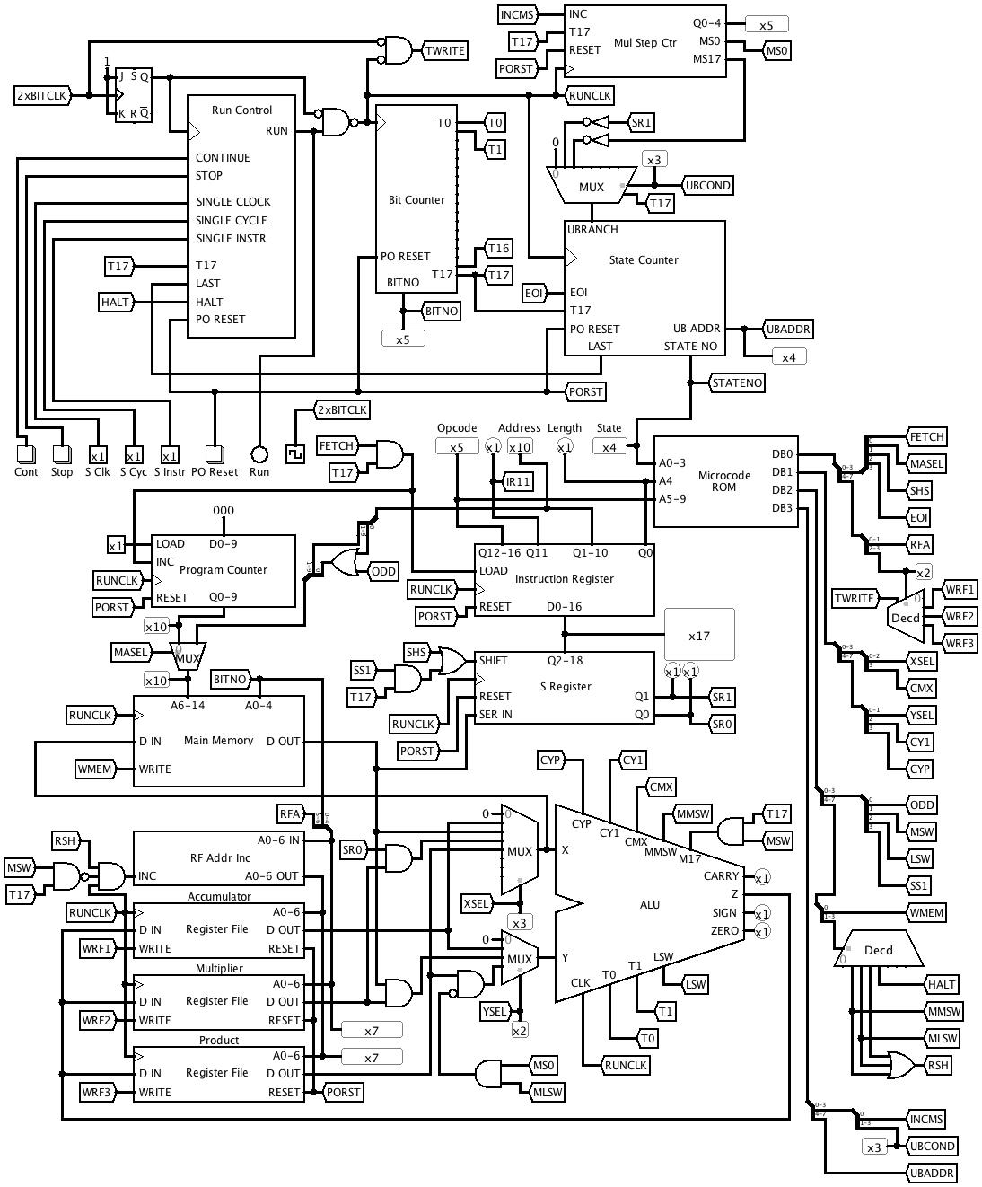
I changed the register file addressing so that the output of the Register Address Incrementer goes only to the Accumulator and Product Register, with the Multiplier Register receiving the unmodified register address. Activating RSH while adding the multiplier to the product then causes bit i+1 of the product to be added to bit i of the multiplier and written back to bit i of the product, thereby performing Product <-- (Product >> 1) + Multiplier.
An AND gate computes the product of the Multiplier with bit 0 of the S Register, and this is made available as an X input to the ALU.
The Product is made available as a Y input through a gate that forces it to zero during the first multiplication step. This allows clearing the Product to be overlapped with the first multiplication step.
The Product is also available as an X input, so that it can be either added to or subtracted from the Accumulator at the end of a Multiply and Add or Multiply and Subtract. The XSEL field had to be widened to 3 bits to allow for this.
I added two control signals MLSW and MMSW to indicate when the least or most significant words of a multiplicand are being processed. To save microinstruction bits, these have been combined with RSH and HALT in a decoded field called MISC:001 MMSW 010 MLSW 011 RSH 100 HALT
Logic has been added to the ALU to perform subtraction during the last bit period of a multiplication if the MSB of the multiplicand is set.
Revised ALU
![]()
Revised Main Circuit
![]()
-
Notes on Multiplication
06/27/2018 at 12:57 • 0 commentsThis is another subject that required quite a lot of thought. I believe I've found a way to make it all work, but there are a number of subtleties involved that I'll try to explain here.
The basic algorithm I'll be using is simple: for each bit of the first operand, multiply the second operand by it, shifted by an appropriate number of places, and add up the results. This is particularly easy to do in binary, since multiplying by a single bit can be accomplished with an AND gate.
In what follows, I'm going to call the first operand the multiplicand and the second operand the multiplier, because the second operand (the one that gets added to the product) will be the one held in the Multiplier Register.Scaling
EDSAC numbers are meant to be interpreted as fractions in the range -1 to 1, and the multiplication algorithm needs to produce results consistent with this interpretation. Given two signed n bit operands with an assumed point between bits n-1 and n-2, we want a 2n-1 bit result with an assumed point between bits 2n-2 and 2n-3.
Here's an example with n = 5:0.75 * 0.6875 = 0.515625 0.1 1 0 0 0.1 0 1 1 ----------------- 0 0 0 0 0 0 0 0 0 0 0 1 0 1 1 0 1 0 1 1 0 0 0 0 0 ----------------- 0.1 0 0 0 0 1 0 0From this we can see that to get a correctly aligned result, the most significant bit of the multiplier (i.e. its sign bit) needs to be aligned with the bit from the multiplicand that we are multiplying it by.
Negative numbers
We need to make sure we get the right results with negative operands.
As long as the multiplicand is positive, we don't need to do anything special -- the multiplier can be of either sign, and as long as we sign-extend it when shifting, two's-complement arithmetic will produce the correct result. For example,0.75 * -0.3125 = -0.234375 0.1 1 0 0 1.1 0 1 1 ----------------- 0 0 0 0 0 0 0 0 0 0 1 1 1 1 0 1 1 1 1 1 0 1 1 0 0 0 0 0 ----------------- 1.1 1 0 0 0 1 0 0
The bits resulting from sign extension are shown in red.
But, we need to be careful when the multiplicand is negative -- naively treating the sign bit of the multiplicand the same way as its other bits will not give the right result.
To see what needs to be done, consider that a number in the range -1 <= x < 0 can be written as -1 + y, where y is what results from taking the bits after the point and interpreting them as a positive number. In other words, we can take the bits after the point as having positive binary weights for both positive and negative numbers, as long as we give the sign bit a weight of -1.
What this means is that we can carry out the multiplication algorithm as usual for the bits of the multiplicand after the point, ignoring its sign; then, if the multiplicand is negative, subtract the multplier from the product. Example:-0.25 * 0.6875 = -0.171875 1.1 1 0 0 0.1 0 1 1 ----------------- 0 0 0 0 0 0 0 0 0 0 0 1 0 1 1 0 1 0 1 1 1 0 1 0 1 ----------------- 1.1 1 0 1 0 1 0 0Here, the bits shown in red result from taking the two's complement of the multiplicand.
Shifting strategy
The above examples are presented as though the multiplier is being shifted to the right by varying amounts, but I'm actually going to do it slightly differently: at each step, shift the product one place right and then add the multiplier to the most significant bits of the product.
This avoids having to shift the multiplier, leaving the contents of the Multiplier Register undisturbed. It also allows me to process the multiplicand bits in order from least significant to most significant, so that I can keep the multiplicand in the S-register and make use of its right-shift capability.
What's more, it turns out that, with a slight modification to the circuitry I already have, I can perform the shifting and adding together in one pass.Where to put the unused bit?
For simplicity, BREDSAC is based on 18-bit cycles. But a short word has only 17 bits, and a long word 35 bits, meaning there is one unused bit in each short or long word. Early on, I chose to put this bit at the most significant end, and extend the sign bit into it. However, while thinking about multiplication, I realised it would be more convenient to put the unused bit at the least significant end.
To see why, consider the 5-bit example from before, extended on the left with an unused 6th bit, shown here in red:0 0.1 1 0 0 0 0.1 0 1 1 --------------------- 0 0 0 0 0 0 0 0 0 0 0 0 0 0 1 0 1 1 0 0 1 0 1 1 0 0 0 0 0 0 0 0 0 0 0 0 --------------------- 0 0.0 1 0 0 0 0 1 0 0
Notice that the product is out by a factor of 0.5. Each of the unused bits adds one extra bit to the product, resulting in it having two extra bits on the left, whereas we only want one. Getting a correctly scaled result would require an extra shifting step at the end.
On the other hand, if we put the unused bit on the right, things look like this:0.1 1 0 0 0 0.1 0 1 1 0 --------------------- 0 0 0 0 0 0 0 0 0 0 0 0 0 0 0 0 0 0 0 1 0 1 1 0 0 1 0 1 1 0 0 0 0 0 0 0 --------------------- 0.1 0 0 0 0 1 0 0 0 0
There are still two extra bits in the product, but they're on the right, where they don't make any difference to the value interpreted as a fraction.
For this reason, I've decided to revise the design so that the unused bit is at the least significant end. In the next instalment, I'll detail the changes required to make this happen.
-
Right Shift Instruction
06/24/2018 at 13:28 • 0 commentsI spent quite a long time thinking about how to implement this instruction. The strategy I eventually came up with is to add 1 to the register file address during the read phase of each bit time. So it reads bit 1 and writes it to bit 0, reads bit 2 and writes it to bit 1, etc. A fair bit of extra circuitry will be required to achieve this, and I don't really like the idea of adding that much complexity just to support one operation, but I haven't been able to think of a simpler way without radically changing the whole design.
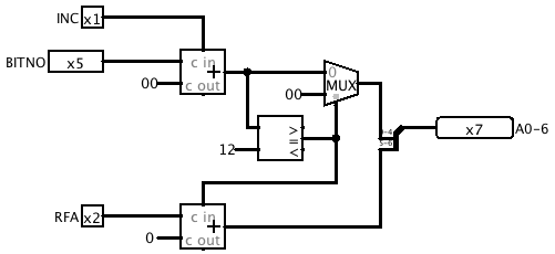
This is the subcircuit I designed to carry out the address incrementing. When the INC input is activated, a 5-bit adder adds 1 to BITNO. If the result is 18 (0x12) the result is forced to zero and a carry is added to RFA![]()
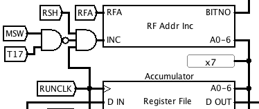
Here's where it fits into the main circuit. A new control signal RSH enables right-shifting behaviour. It is gated with RUNCLK so that the register file address is incremented during the read phase of each bit time. Incrementing is disabled during T17 of the most significant word, so that the most significant bit is unaltered. This makes the operation an arithmetic shift (i.e. with sign extension)
![]()
Microcode
This is the microcode for the right shift instruction. It uses the same technique as the left shift for keeping track of the number of places to shift.
# OPCODE L STAT : FETCH MASEL SHS EOI RFA WRF XSEL YSEL  CMX SS1 CY1 CYP ODD MSW LSW HALT WMEM UBCOND UBADDR RSH

# R - Right shift
   00100 x 0001 :   0     0    0   0   00  10   10   00   0   0   0   0   0   0   1   0    0    000    0000   1
   00100 x 0010 :   0     0    0   0   10  10   10   00   0   0   0   0   0   0   0   0    0    000    0000   1
   00100 x 0011 :   0     0    0   0   01  10   10   00   0   0   0   0   0   0   0   0    0    000    0000   1
   00100 x 0100 :   0     0    0   1   11  10   10   00   0   1   0   0   0   1   0   0    0    100    1000   1
Glitches, Will Robinson!
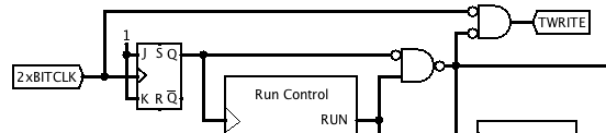
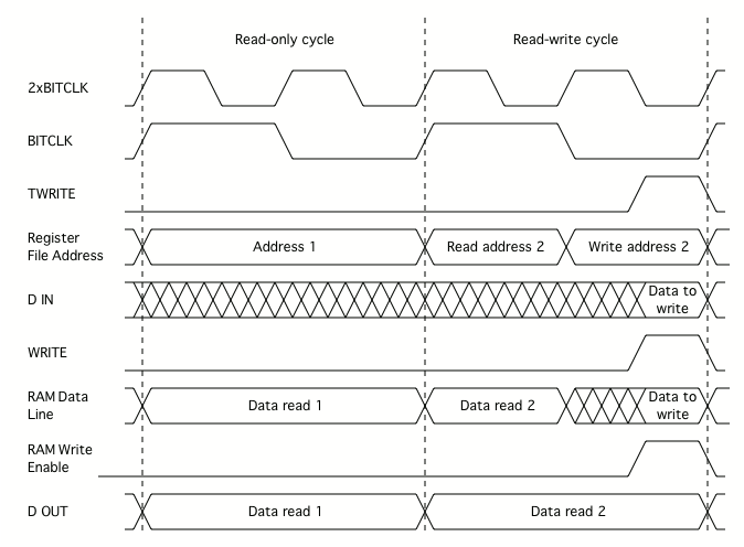
Testing in Logisim revealed a problem with this arrangement. Previously, the register address only changed on the rising edge of BITCLK, and was stable at the leading edge of the WRITE signal to the register file, but now the register address can also change on the falling edge of BITCLK. This was causing spurious bits in the accumulator to change.
To fix this, I changed the clocking arrangement. The simulation is now clocked at twice the BITCLK rate, and a timing signal TWRITE is derived that is active during the last quarter of each bit period. This is used to gate the WRF1-WRF3 signals, which delays writing to the register file until a quarter of a bit period after any potential address change![]()
![]()
Revised register file timing:
![]()
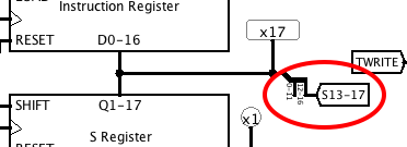
 LDPC causes the program counter to be loaded from the address field of the instruction register:
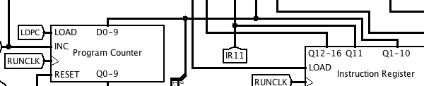 Here is the microcode for the jump instructions. Each one consists of just a single microinstruction that passes the accumulator through the ALU and activates JUMP together with the appropriate condition.