-
1▇▇▇▇ Understand Synchronous Logic ▇▇▇▇
Clocks are an important part of practical digital design. Suppose you have a two input
ANDgate. Then imagine both inputs go from zero to one, which should take the output from zero to one, also. On paper, that seems reasonable, but in real life, the two signals might not arrive at the same time. So there’s some small period of time where the output is “wrong.” For a single gate, this probably isn’t a big deal since the delay is probably minuscule. But the errors will add up and in a more complex circuit it would be easy to get glitches while the inputs to combinatorial gates change with different delays.The most common solution to this is to only “look” at the signals (and store them in a flip flop) on a clock edge (usually, just the rising edge). Now the circuit will work fine if the longest delay from one flip flop’s output to the next flip flop’s input is less than the period of the clock. This makes things much simpler to design.
If you need a refresher on flip flops, they are elements that remember a single bit. A D flip flop will remember its input (named D) at the clock edge and hold that output until the next clock edge. There are other kinds of flip flops, like the T flip flop (which toggles state) or the JK flip flop which can perform several functions. With Verilog, you generally won’t create flip flops directly, but will let the compiler infer them from your code.
Let’s jump right in with some examples. I’ll explain these each in more details as we go. Consider this code:
reg myoutput;
wire myinput;
always @(posedge clk)
   myoutput<=myinput;
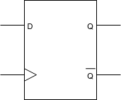
This would infer a D type flip flop.
![]()
When the clock (the wedge-shaped symbol on the schematic) rises, the D input will appear on the Q output. The lower Q has a bar above it and will always be the inverse of the Q output.
The compiler will recognize other types, too. For instance:
reg myoutput;
wire myinput;
always @(posedge clk)
   myoutput<=myinput?~myoutput:myoutput;
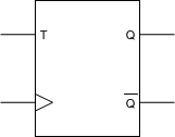
This would infer a T flip flop. Where Q toggles -- that is goes from 1 to 0 or 0 to 1 -- on each rising clock. If you know C or a similar language, you probably know the ? operator and the ~ operator. If not, the ~ inverts all the bits. The ? operator is a bit trickier. You can think of it as an "if-then-else" construct. If the first part is true, the result is the expression between the question mark and the colon. Otherwise, the result is the part behind the colon. For example, the value of 4>3?2:1 would be 2 because 4 is greater than 3. If we had used 4<3?2:1 the value would be 1.
![]()
Usually, though, the inference of a flip flop is not this direct. The input might be a logic expression. The compiler can also infer counters which are lots of flip flops:
reg [3:0] ctr;
always @(posedge clk)
begin
  if (ctr_reset) ctr<=4'b0; else ctr<=ctr+1;
end
This code creates a 4 bit counter. On each clock edge it computes ctr+1 as the new count value unless ctr_reset is true.
Just as using the plus operator allowed the Verilog compiler to do the best thing for an adder, the expression above will let it build an efficient counter without you having to worry about the details. You can build a counter out of individual modules that infer flip flops (or modules that your tool provides for you) but it is better to leave the details to the compiler.
-
2▇▇▇▇ Build a Flip Flop ▇▇▇▇
The demo circuit has three distinct parts: the binary adder circuit from last time is already done. Another part of the example design is to provide an output that latches when a carry is generated. Here’s the part of the code that does that:
reg carrylatch;
// latch carry result
always @(posedge clk)
begin
   if (reset==1'b1) carrylatch<=1'b0;
   else begin
     if (carry) carrylatch<=1'b1;
   end
end
In English, this says that when the clock has a rising edge, check to see if the reset line is high. If it is, clear the carry latch. Otherwise, check to see if the carry is set and if so, set the carry latch. It will remain set until a reset clears it.
The Verilog tool will recognize this is a flip flop with synchronous reset. If you get really concerned about performance, you may want to investigate if your FPGA does better with an asynchronous reset and learn how your tool can be told to do that instead. But for now, this is sufficient. The realization will probably be a D type flip flop with a rising edge-sensitive clock input and a clock enable tied to the carry line. The D input will be tied to a logic 1.
-
3▇▇▇▇ Key Point #2: Assignments ▇▇▇▇
(By the way, if you are wondering where Key Point #1 is, it is in Bootcamp #1.)
Did you notice that some assignments use
=and some use<=? This is an important Verilog feature. When you are using assignments, you always use the equal sign. If you are writing a sequential block, you almost never want to use the single equal sign, even though Verilog will allow this. Here’s why:always @(posedge clk) begin a<=1’b1; b<=a; end
Because the nonblocking assignment (
<=) appears, the value of b will become whatever a was at the moment the clock edge occurred. That is, all the assignments in the block happen all at one time. In simulation, that means they happen at the end statement since simulations have to pretend everything happens in parallel. In an FPGA, parallel execution is just how the hardware works.<=
The problem occurs if you do not use a non-blocking assignment. Suppose we had:
always @(posedge clk)
begin
  a=1’b1;
  b=a;
end
The Verilog compiler is smart enough to know that b should equal 1 in this case and has to generate extra circuitry (a latch) to make sure b isn’t set at the same time as a. This can cause lots of timing issues and unless you are sure you need to do it and understand the ramifications, you should avoid it at all costs.
-
4▇▇▇▇ Key Point #3: Default Net Types ▇▇▇▇
You may notice that some of the variables in the Verilog code are of type wire and some are of type reg. A wire has to be constantly driven to some value. A reg is more like a regular variable. A reg may, but doesn’t always, infer a flip flop. However, you can set a value in a reg and it sticks.
One problem you wind up with in Verilog is that if you make up a name, the compiler (by default) will assume you mean for it to be a wire unless you tell it otherwise. That sounds handy, but the problem is if you misspell a name, it just becomes a new wire and then you can’t figure out why your code doesn’t do what you want.
The answer is to always include this at the front of a Verilog file:
`default_nettype none
This causes the compiler to throw an error if you use an undeclared net. That will save you a lot of debugging time wondering why things aren’t working.
-
5▇▇▇▇ Counting and Dividing ▇▇▇▇
The remainder of the Verilog takes the 12MHz clock and uses it to drive a 16 bit counter. When the counter overflows, another counter increases. When that counter reaches 91, the secondary counter goes to zero. This takes roughly 1/2 second at 12MHz.
You can figure that out by noting that 12MHz is 83 ns or .000083 us. A 16-bit counter will overflow on the 65536th count (two to the 16 power). Do the math and that comes out to nearly 5.5ms per overflow. If you let the secondary counter go to 91, that will take almost 497ms. If you go to 92, you go over (502 ms). Note that counting to 91 (or 92) only takes a 7 bit counter. A graphical representation of the situation is shown here with the code for it below.
![]()
// The 12MHz clock is too fast
// The first counter will / 2^16 (about 5.46ms)
// Then the second counter goes to 91 which is 0.497s
// close enough to 1/2 second for our purpose
always@(posedge clk)
begin
if (reset==1'b1)
begin
   cnt1<=0;
   cnt2<=0;
   half_sec_pulse<=0;
   dec_cntr<=0;
end
else if (runstop==1'b0) // don't do anything unless enabled
begin
   cnt1 <= cnt1 + 1;
   if (cnt1 == 0)
     if (cnt2 == 91)
       begin
         cnt2 <= 0;
         half_sec_pulse <= 1;
       end
    else
      cnt2 <= cnt2 + 1;
   else
     half_sec_pulse <= 0;
   if (half_sec_pulse == 1)  dec_cntr <= dec_cntr + 1; // count half seconds
   end
end
By the way, there's nothing magic about making a 16-bit counter and a 7-bit counter. I just wanted to show an example of two different pieces. In a real design you might do this because you need a faster signal and a slower signal. In addition, in some cases, longer counters can have problems at certain frequencies.
This is a form of sequential circuit and the counters will turn into a chain of flip flops when synthesized. Here’s the definition for the counters:
// Manage 12MHz clock
reg [15:0] cnt1;
reg [6:0] cnt2;
reg [1:0] dec_cntr;
reg half_sec_pulse;
The counter declarations look like arrays, but they aren’t (Verilog does support arrays, but these are not arrays). The numbers in square brackets are telling you the number of bits in the value. So cnt1 has 16 bits numbered from 15 (the most significant) to 0 (the least significant).
We’ll use the array-like bit notation and the assign statement to make some LEDs blink too:
// Make the lights blink
assign LED4 = (dec_cntr == 2);
assign LED5 = dec_cntr[0];
-
6▇▇▇▇ Understanding Clock Division ▇▇▇▇
At these clock frequencies, this technique of dividing down the clock is OK, but usually you'd rather use the FPGA's clock circuitry like a PLL or DLL to generate different timings, if possible. How you do this will depend on your FPGA and won't work in a generic simulator like we are using.
Also, you don't want to ever divide a clock and then try to use it as a clock to another element. Some FPGAs can support this, but it is almost always a bad idea. The reason is, the FPGA will have special busses just for clocks. If you try to take the output of a flop and feed it into a clock bus, it will be at best inefficient and at worst impossible. Instead you wind up running everything off one clock, if possible, and then enabling the clock when you want. For example:
// divide clock by 16
reg [3:0] clk16ctr;
wire clk16;
assign clk16=clk16ctr==4'b1111];
always @(posedge clk)
   begin
      if (reset) clk16<=4'b0;
      else clk16<=clk16+4'b1;
   end

// Now we want this to happen on clk16
always @(posedge clk)
   if (clk16)
    begin       // This happens on every 16'th tick    end
If you are following along you want to make sure all the new code is in the design.sv or design.v tab to the right simulator (the code is already there if you click that link). If you are using a local simulator like Icarus on your own computer, you just need to grab the files from the file section of the project.
-
7▇▇▇▇ Update the Test Bench ▇▇▇▇
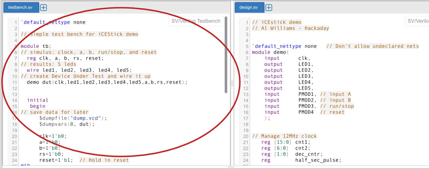
With new stuff in the design, we need to update the test bench to exercise it. In particular, since the new design requires a clock, the testbench has to provide it. It would be very annoying to have to write each clock transition. Luckily, you don’t have to. Here’s how the clock generation works:
always
begin
#1     clk<=~clk;
end
In English, this says: At all times, you should delay one clock cycle (the #1) and then invert the clock signal and keep doing that forever. Another item to consider is the FPGA reset:
rs=1'b0; // run/stop
reset=1'b1;
#10
reset=1'b0;
This bit of code sets the reset line, holds it for 10 clock cycles, and then clears it.
At the end of the test bench is a 400 cycle delay just to let the counters do something.
You'll need to make sure the code is correct in the right-hand pane of the simulator or your testbench file if you are using a stand alone simulator.
![]()
-
8▇▇▇▇ Simulation Specifics ▇▇▇▇
There’s one small problem with the simulation. The 12 MHz divider won’t do anything interesting in “only” 400 cycles. It isn’t uncommon to change magic numbers to smaller values when simulating. In this case, I change the primary counter increment to 8000 hex so it will flip every other clock cycle and then changed the test for 91 down to a more reasonable value.
There are several ways you can do this, but to stay simple, I just commented out the real versions and later I’ll remove the comments and comment out the simulation versions.
You can see the section of code you need to change back and forth below:
![]()
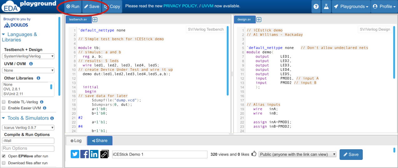
Then you can use the Save/Run buttons to start the simulation.
![]()
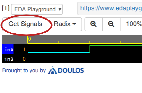
Once the EPWave screen appears, you can use the Get Signals button to pick the signals you want to see.
![]()
![]()
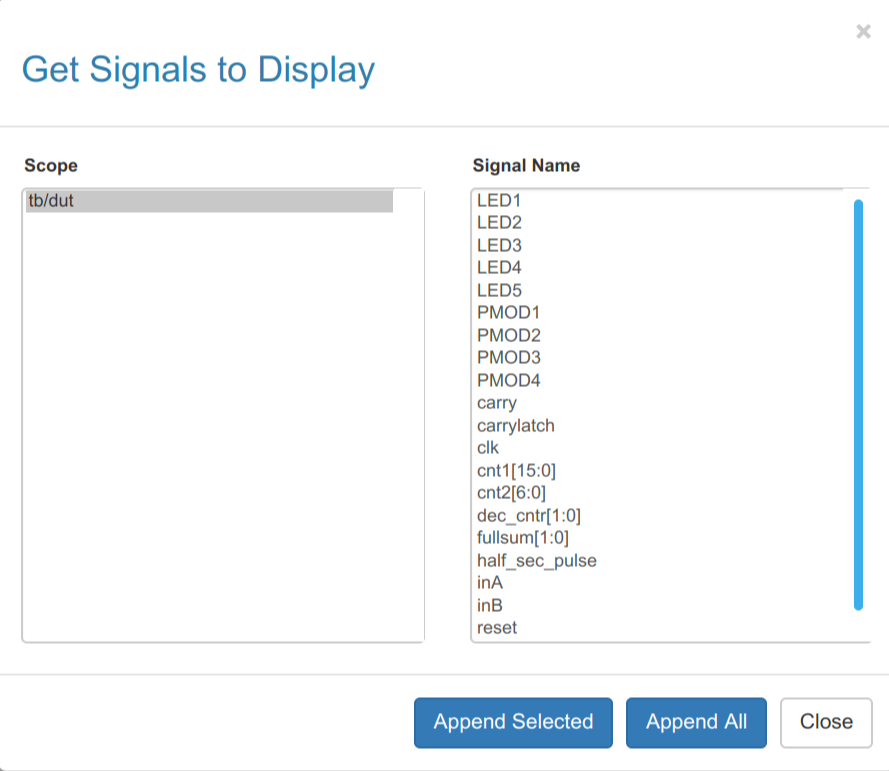
You can pick the signals below, although the order isn't really important. Press Append Selected when you have them all. Or, if you don't mind some extras you can press Append All.
![]()
Don't forget that we changed the timing, so the LED "blinking" won't be at 1/2 second unless we restore the original code and wait a long time for the simulation to complete.
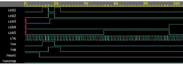
You can see the entire code on EDAPlayground and you can even run the simulation from there. The waveform shown here will appear. If you want to know more about how it all works, check out the video below and I’ll walk through it step by step. Note: the video may use a different Verilog simulator, but since we are using standard Verilog features, it should not make any difference.
 Al Williams


Discussions
Become a Hackaday.io Member
Create an account to leave a comment. Already have an account? Log In.