-
A Quick FPGA Glossary
07/12/2018 at 18:29 • 0 comments- Adder - See Full Adder and Half Adder.
- AND Gate - A gate who's output is 1 only when all inputs are 1.
- Blocking assignment - In Verilog, when an assignment occurs before any subsequent assignments (that is, it does not occur in parallel).
- Combinatorial Logic - Logic that does not rely on the previous state of the system to set the current output state.
- Exclusive OR Gate - See XOR Gate.
- Flip Flop - A circuit element that can take one of two states (1 or 0) and remember it until changed. Somewhat like a one-bit memory device.
- Full Adder - A circuit for adding two binary numbers and a carry bit (so three bits overall). It will produce a sum and a carry.
- FPGA - Field Programmable Gate Array.
- Half Adder - A circuit for adding two binary numbers. It will produce a sum and a carry
- Inverter - See NOT Gate.
- IP - Intellectual Property. Typically a third party module that does a particular function that you can integrate into your FPGA designs if you wish.
- Logic Diagram - See Schematic.
- Non-blocking Assignment - In Verilog, when an assignment occurs in parallel with other assignments in the same block.
- NOT Gate - A gate that takes a single input and inverts it. That is, a 1 becomes a 0 and a 0 becomes a 1.
- OR Gate - A gate who's output is a 1 if any inputs are 1.
- Schematic - A diagram of a logic circuit made up, usually, of logic symbols for fundamental gates.
- Sequential Logic - Logic that typically uses flip flops and the current output state influences future output states.
- Testbench - Verilog (or similar) code that exists only to send stimulus to a simulated device and record or test the results.
- Truth Table - A table showing a logic circuit's possible inputs and the outputs that will result.
- Workflow - The process of taking design inputs and producing a working FPGA configuration.
- Verilog - A description language used to describe logic you wish to place on an FPGA.
- VHDL - A description language (not used in this bootcamp) to describe logic you wish to place on an FPGA.
- XOR Gate - Exclusive OR gate. A two-input gate that sets its output to 1 if either input is a 1, but not when both inputs are a 1.
Logic Truth Tables for Two-Input Gates
A B AND OR XOR 0 0 0 0 0 0 1 0 1 1 1 0 0 1 1 1 1 1 1 0 -
A Brief Introduction to Sequential Logic Design
07/10/2018 at 22:26 • 0 commentsCombinatorial design is easy to understand with AND, OR, and NOT gates doing most of the work. These designs are great for things where the previous state of the system doesn't matter. For example, imagine a car with an interior dome light. You want the light to come on if any of the doors are open (D1-D4) or the dashboard switch for interior light is on (S1). You can express that with an OR gate (or the | sign which is typically used for OR) Z=D1|D2|D3|D4|S1. Or perhaps you want all those conditions but only if a sensor says it is dark (X1). Then you could do an AND (&): Z=X1&(D1|D2|D3|D4|S1).
However, consider the car's alarm. It might also look at D1, D2, D3, and D4. But what it does will depend on if the system is armed or not. Let's take the simplest case. The system should arm if it gets a pulse from the keyfob receiver K1. Another pulse will disarm it. While the system is armed, any input from D1, D2, D3, or D4 should set off the alarm. There's a problem with this, but let's look at it first before we work on the problem.
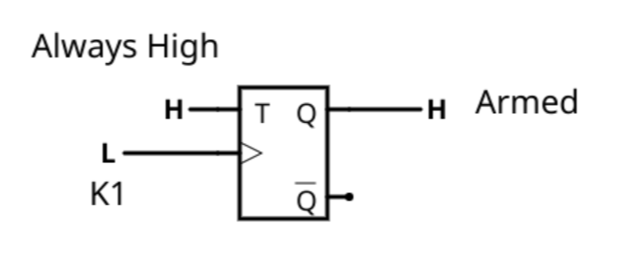
The arming/disarming can be done with a T flip flop. This is the kind of flip flop that toggles its output with each clock pulse. So for example, if you forced the T input high you could connect K1 to the clock and the Q output would tell you if the system is armed or not (try it on Falstad).
![]()
Now it would be simple to use a 4 input OR gate and an AND gate
![]()
That works (try it on Falstad).
However, there is a slight problem. When you open a door and the system is armed, the alarm goes off as it should, but once you close the door, the alarm goes off again. Not ideal.
To fix that you need another flip flop that remembers the alarm is on until the alarm is disarmed. You can try that on Falstad too:
![]()
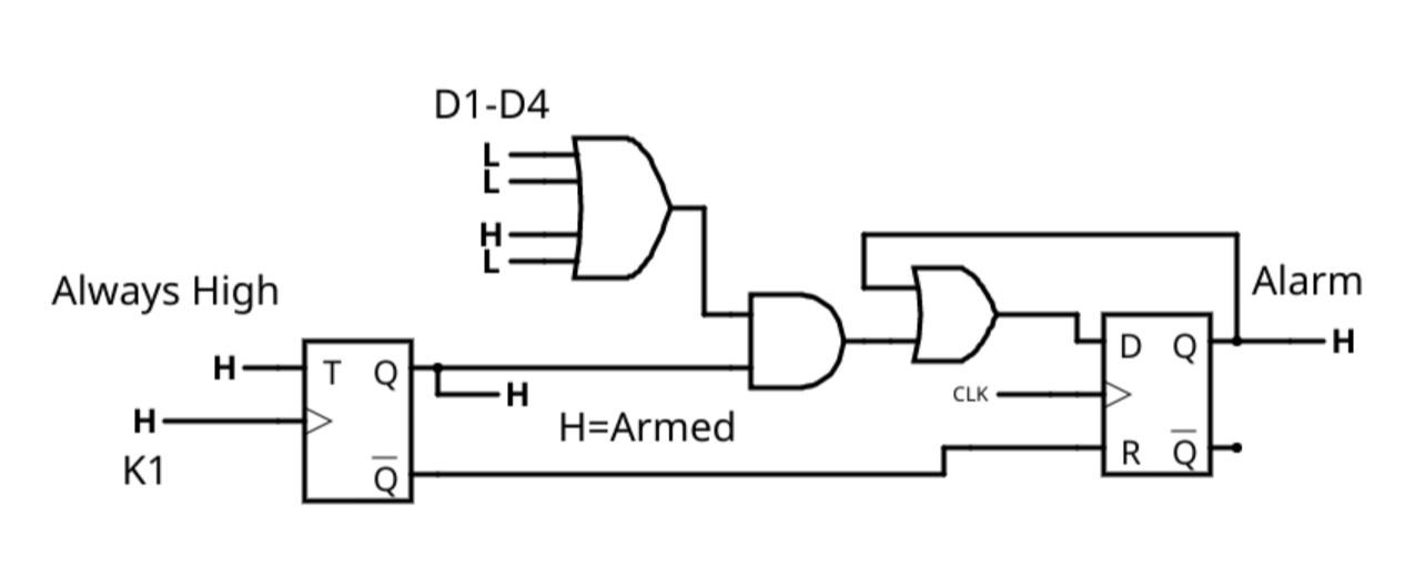
This is a bit odd because of the way it is clocked. In this case, the K1 signal is the clock for the T flip flop. The D flip flop uses a little delay (two inverters) to ensure the D line is stable by the time the clock edge rises. The R pin on the D flip flop is a reset and any time the system is not armed, it forces the output of the D flip flop to be low.
In most FPGA systems, you will have one (or sometimes a few) master clocks. For example, consider this circuit:
![]()
This is essentially the same as the last circuit, but the D flip flop now has a clock that runs all the time. If a door managed to open and close faster than the clock period, the alarm would not trigger! Of course, if the clock were, say, 10 MHz, there would not be much chance of that really happening. The OR gate in front of the D flip flop makes it "stick" on. That is, once Q goes high, it will stay high until the reset forcibly turns it off.
So what do flip flops do for you?
1) They give your circuit memory, like in the above example.
2) They provide a fixed time for inputs to stabilize before producing an output. This is discussed more in the main portion of the tutorial.
Flip flop "memory" allows you to create things like counters, registers, and state machines -- topics for future bootcamps.
-
Connecting I/O
06/23/2018 at 03:04 • 0 commentsIn the last bootcamp and this one, we've connected to things like LEDs and clocks. But how does Verilog know where those things are? The answer is right now, it doesn't. If you don't do anything, the tools will assign the pins anywhere it wants and since we already have a PCB with clocks on some pin and LEDs on some pins, that just won't do.
The Verilog right now isn't being configured to go to the chip. So whatever names we decide on match up in the design and the testbench and that's fine. But in the next bootcamp that won't be good.
Each tool has a slightly different way of handling things, and we'll talk about the tool we will use in the next bootcamp. But, in general, all tools will have some way to create constraints. Most tools can take lots of different kinds of constraints and one of them can be used to define I/O mappings.
What's a constraint? Remember once your Verilog is processed, the tools will map what you have asked for into blocks the FPGA has and then figure out how to connect them together. A constraint tells the system something it must do during that process. Of interest to us now is to say "Hey, the signal called clk needs to be in an I/O buffer that connects to pin X." The router will be sure that happens as it juggles around trying to find the best way to lay out the design.
There are other kinds of constraints. For example, you might tell the system that the timing between two points has to be no more than 20 nS, for example. Or that two blocks need to be put next to each other. That's pretty rare, but sometimes you need it. In particular, you will usually provide a clock constraint that will tell the tool the clock frequency you intend to use and it will tell you if you have delays that would cause problems. This is known as "not meeting timing" and we'll talk about it a lot in a future bootcamp.
How do you set these constraints? That depends on the tools. Common tools will let you put special comments in the Verilog file or provide a text file with constraints in it. Some tools will have a GUI that can build or edit that text file, too -- some will have a few choices of GUIs.
Again, we'll look at exactly how this works for the IceStick in the next bootcamp, but I wanted you to be aware of the necessity and importance of this no matter which tools you are using.
 Al Williams


