 mmca
mmca-
1V3.1 Build instructions
I would like to apologize for the delay, I was crazy to think I would have time to work on the project over the holidays. But the delay did allow us to include a programmer with the kit, so that's nice.
We are going to assume you are familiar with basic soldering techniques, but will include some help for the more unique soldering challenges this build presents.
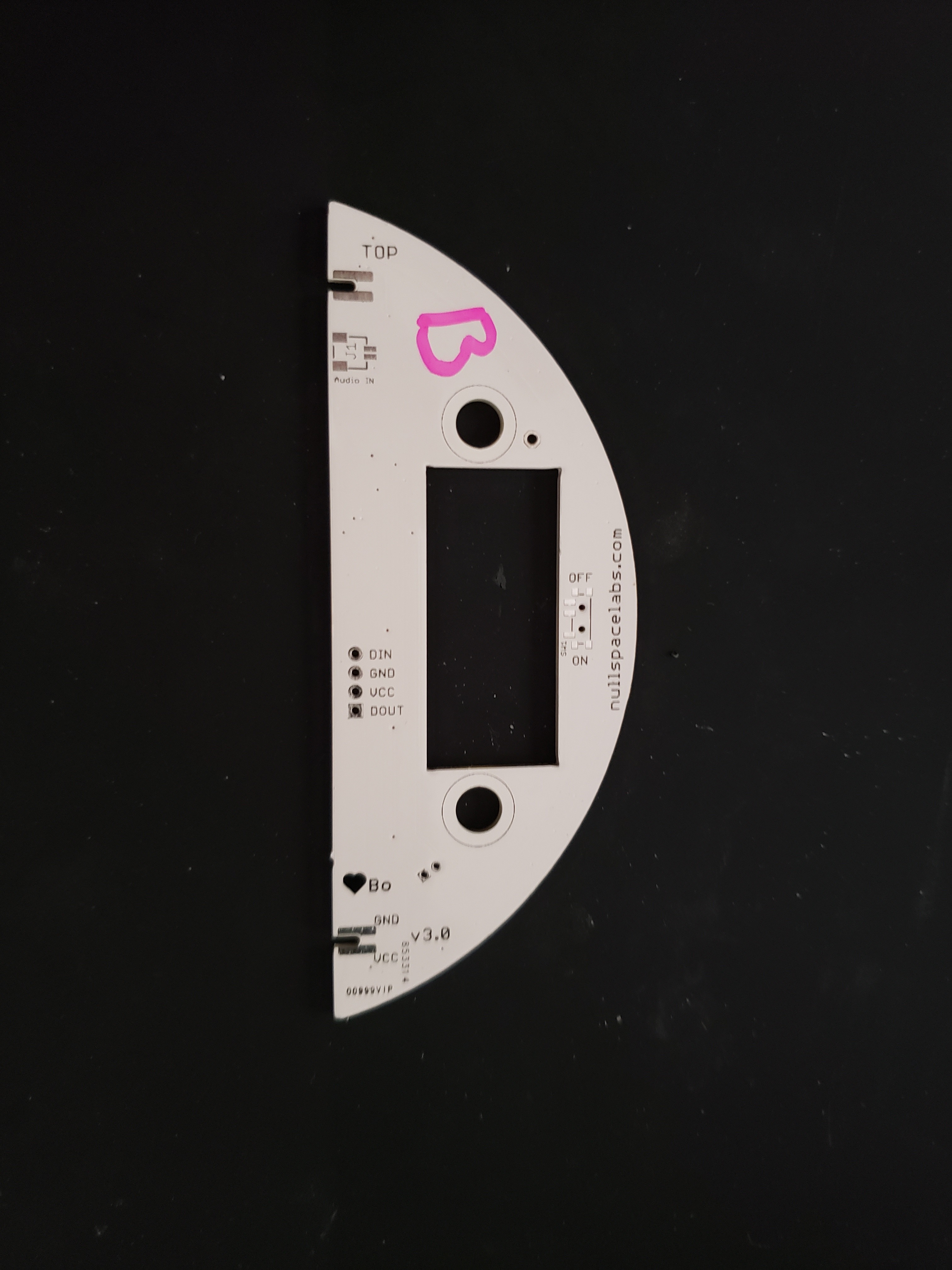
Included in the kit is one slice marked with a pink B, we will use that to assist in the soldering of the LEDs.
![]()
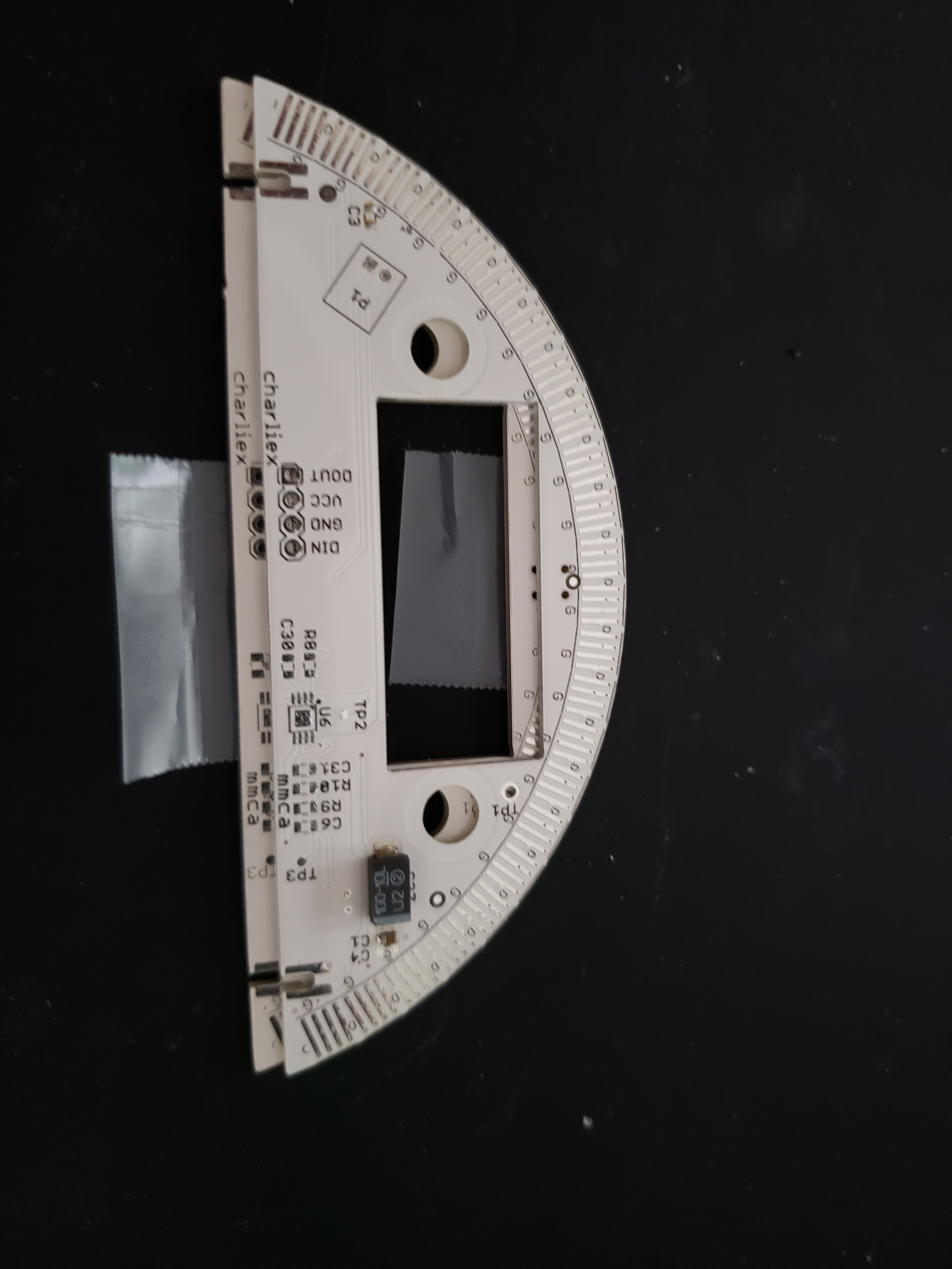
Place one of the sub slices on top of the 'B' slice, like so.
![]()
Secure them together with a little bit of tape.
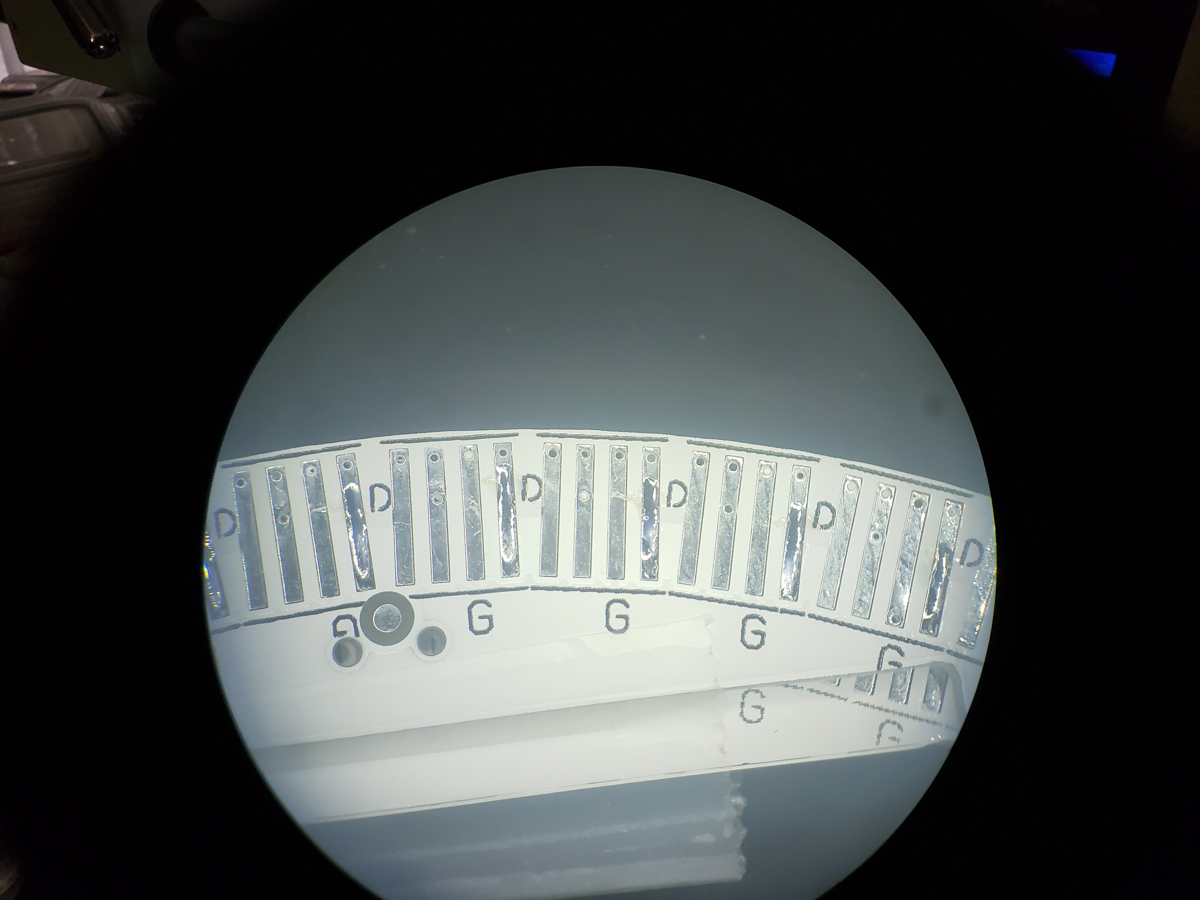
Tin one of the pads for the LED. I like to do one pad of each LED first, but you can do them one at a time.
![]()
Add some flux and attach to pre-tinned pad. Once it is secured, finish soldering the LED on. There is a little 'D' next to each pad, to denote the direction of the LED. The LEDs have a flat side and a round side. If you are unsure, take a look at the populated main slice, the orientation is the same.
![]()
-
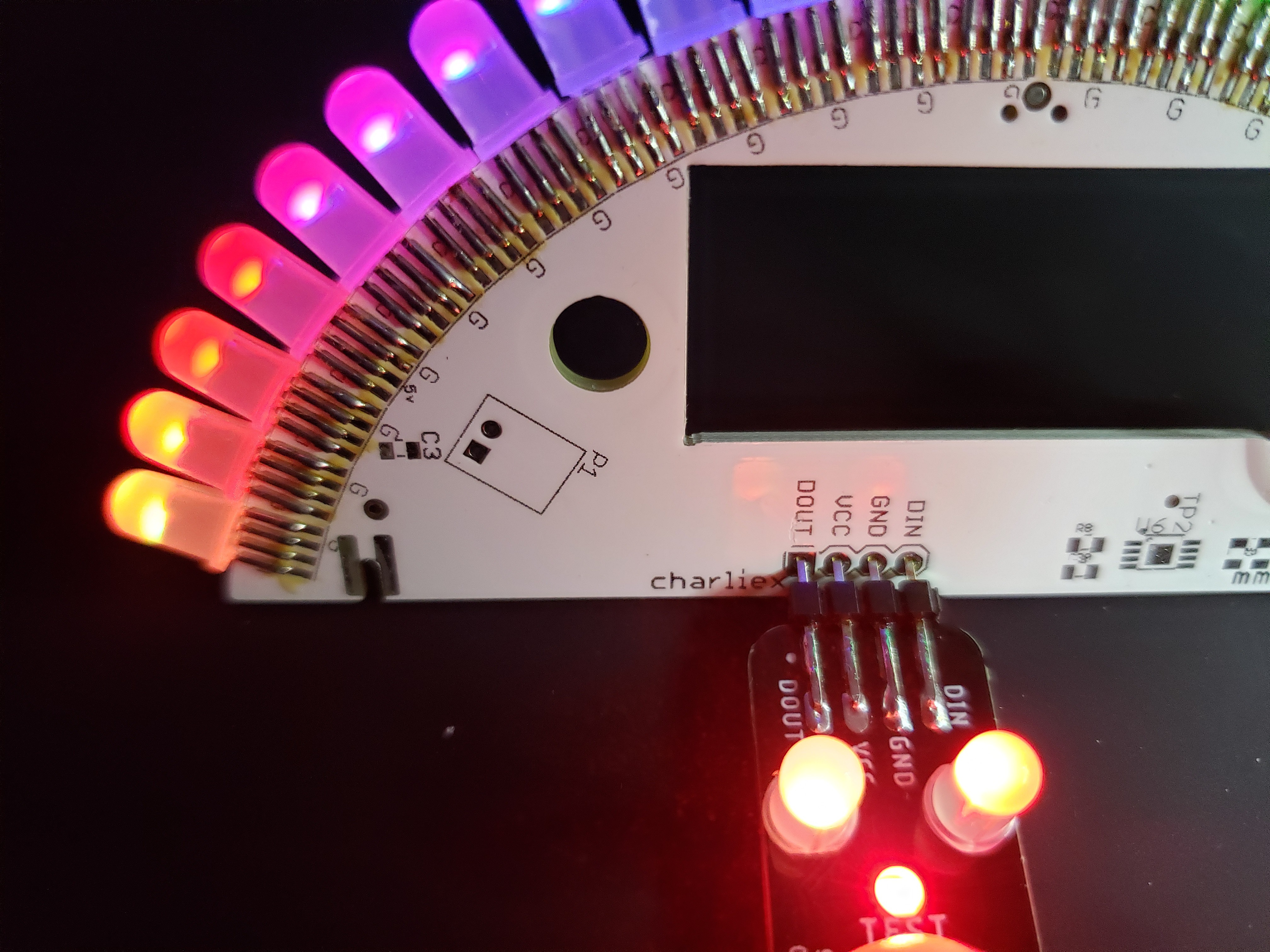
2Testing the slice.
Included in the kit is a slice tester. It maybe white or black like the one in the pictures.
Connect it to USB power using a micro-USB cable. And connect to your completed slice like so:
![]()
When connected and the TEST button is pressed, the signal will go from the tester to slice and the signal will return to the tester completing the circuit. Both RGB LEDs on the tester should light up.
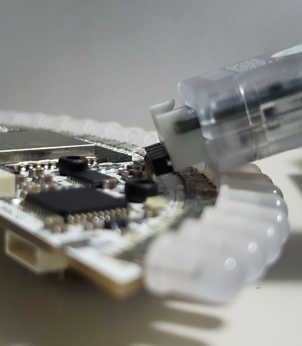
If one of your LEDs on the slice does not light up and needs to be removed (either to be flipped or completely changed out. I would recommend they be removed like so:
![]()
Add a glob of solder that touch all four pins, heat of the glob and remove the LED. Clean the pads, add a little flux and re-solder on the LED.
-
3Programming Header PIns
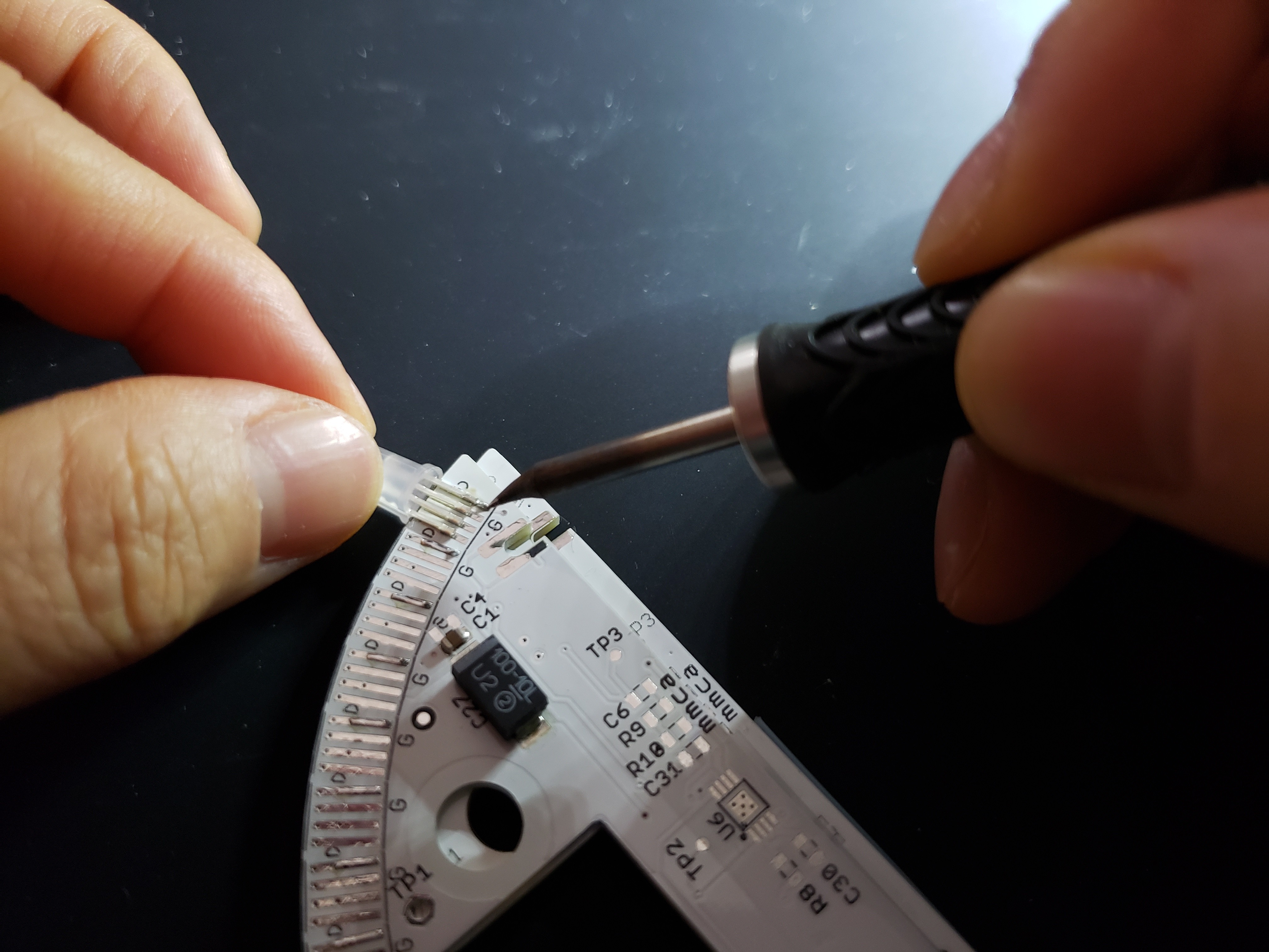
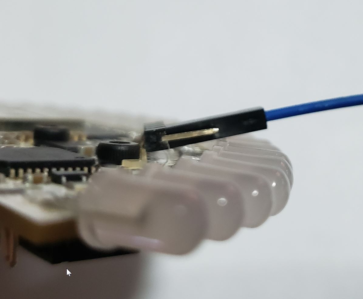
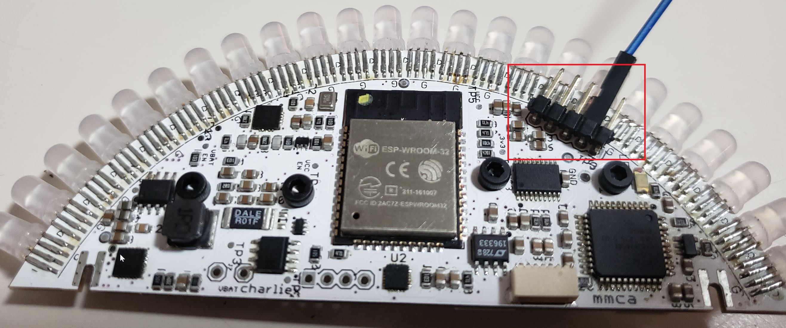
If you have a Cypress PSOC programmer, you will want to solder the programming pins in with a little extra clearance.
![]()
If you intend to just use the programmer supplied, you can just leave enough clearance for a jumper wire.
![]()
![]()
-
4Top and Bottom caps
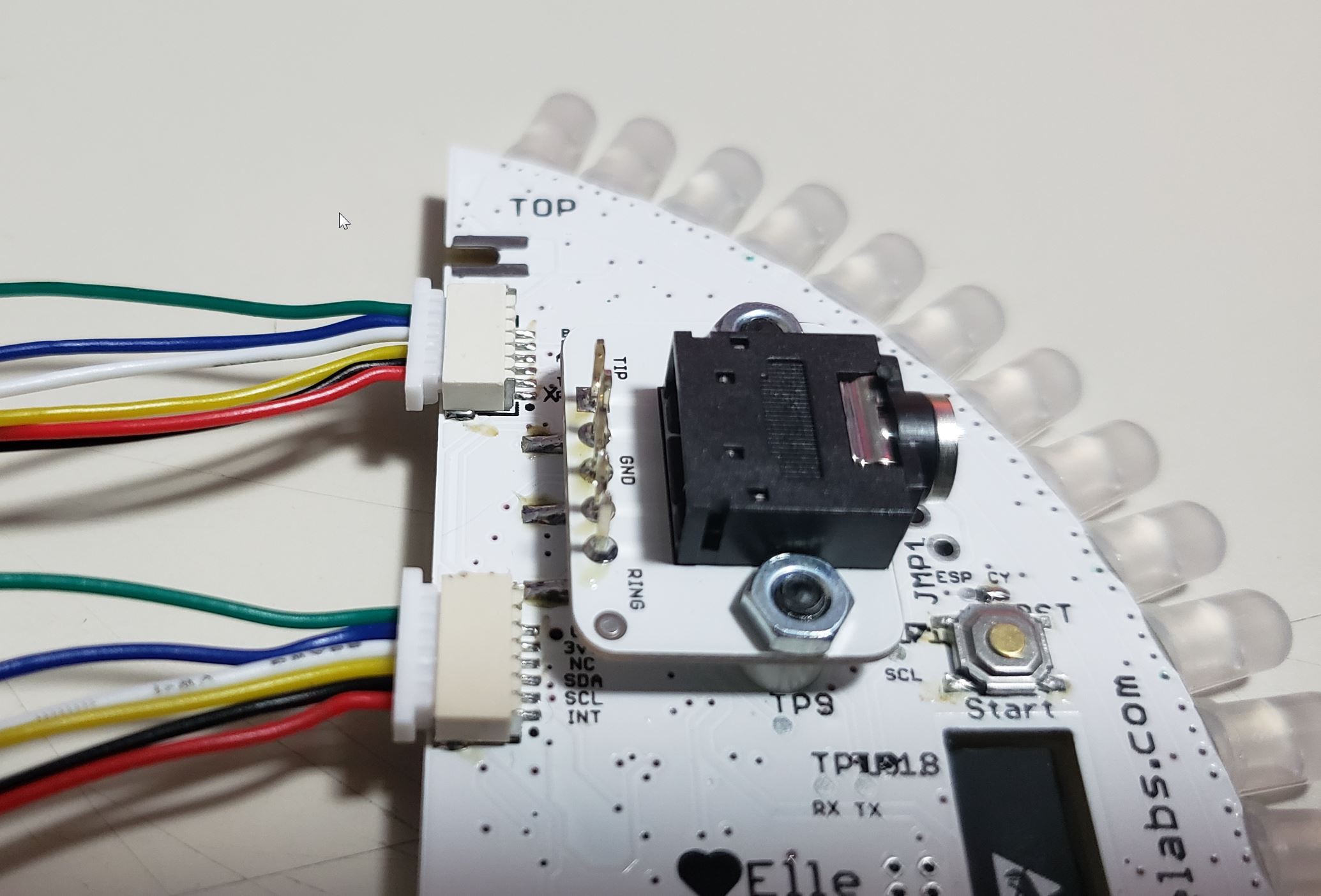
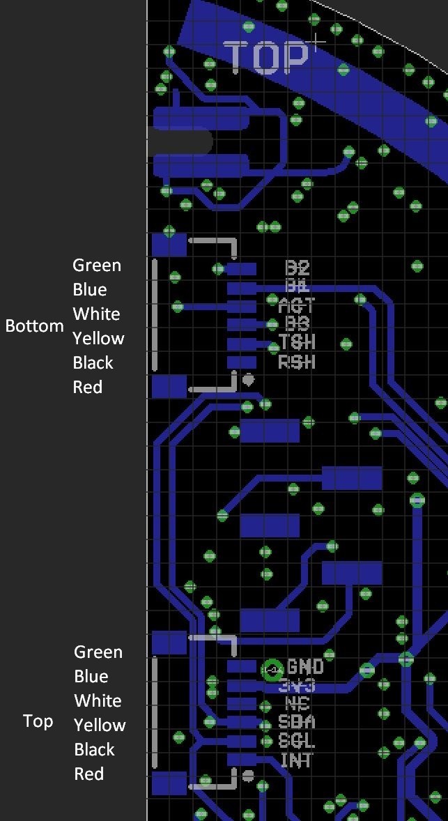
On the main PCB, the top connector goes to the bottom cap PCB and the lower connector goes to the top cap PCB.
This allows for the connector wires to be a little longer and not strain making a sharp turn.
(There is an error in the silk screen, TSH is supposed to be B3 and RSH is GND.)
![]()
![]()
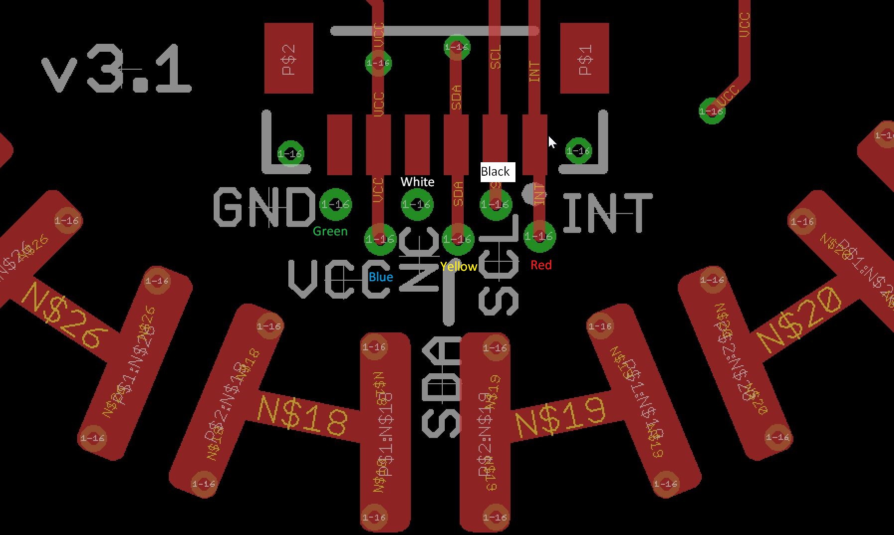
The top cap has 6 connections, trim the wires supplied and solder like so:
![]()
The bottom has 8 connections, 5v and power GND along with 6 signals. Trim the supplied connector wire and solder like so:
![]()
The power (5v and GND) will be connected in the next step.
There is a connector on the other side of the board, it is for testing the sound output before we add the head phone jack. It is not used in the build.
----
Alternate Build
We have included 2 SMD female connectors that can be soldered on, and the extra wires can be spliced together to make a double ended connector wire. In our test builds people found it easier to do the above, but you may want to use the SMD connector.
-
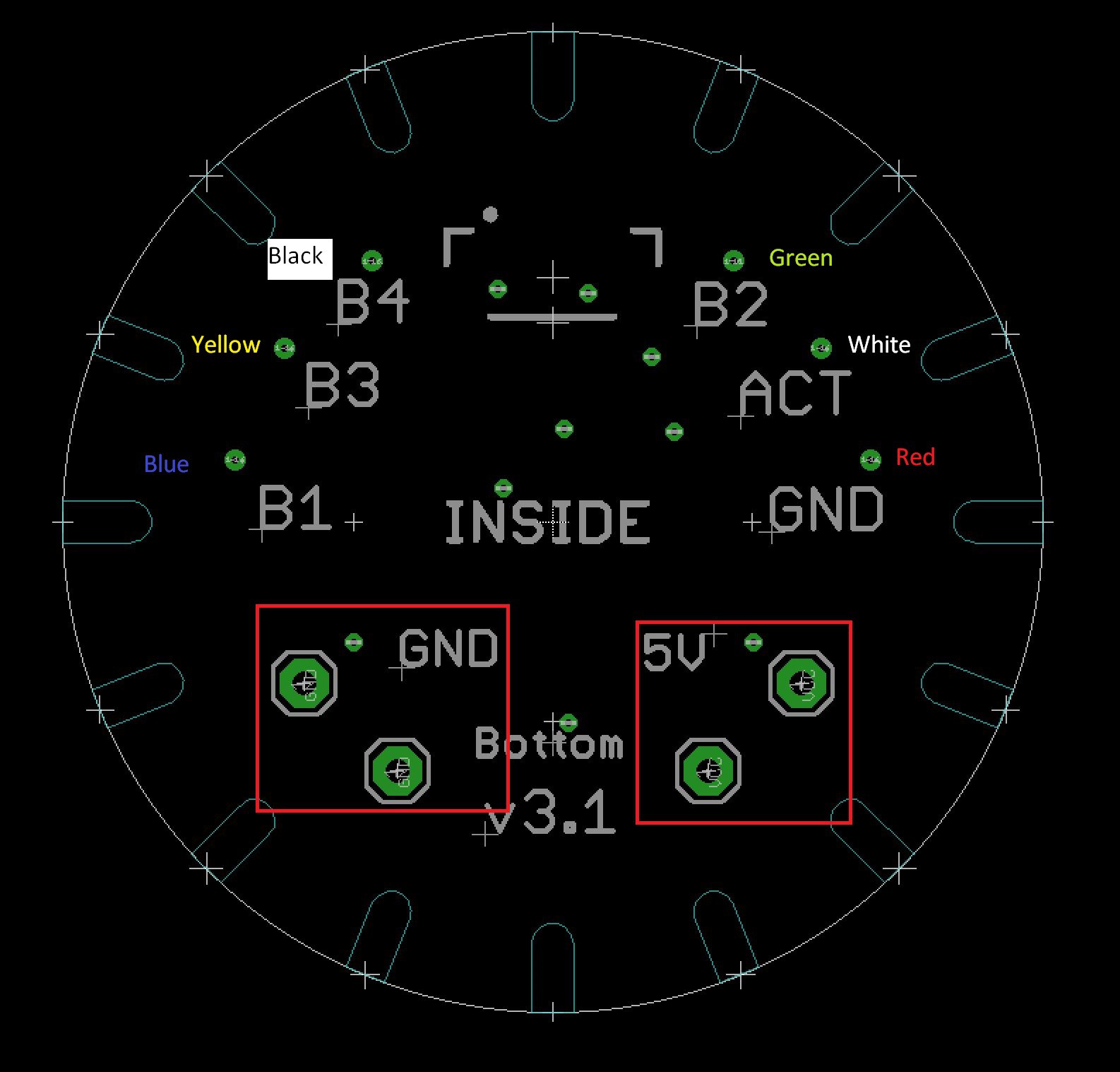
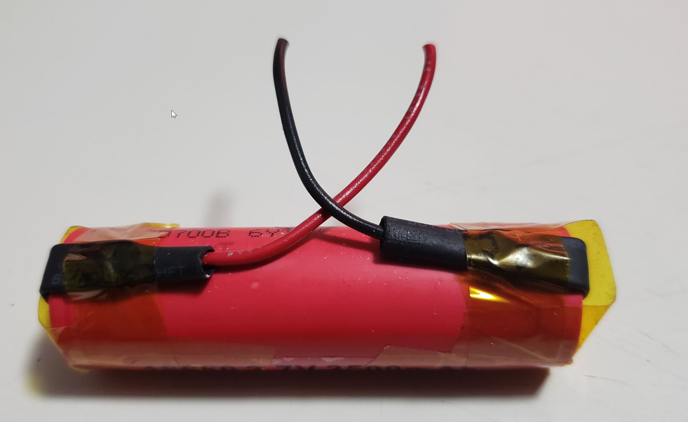
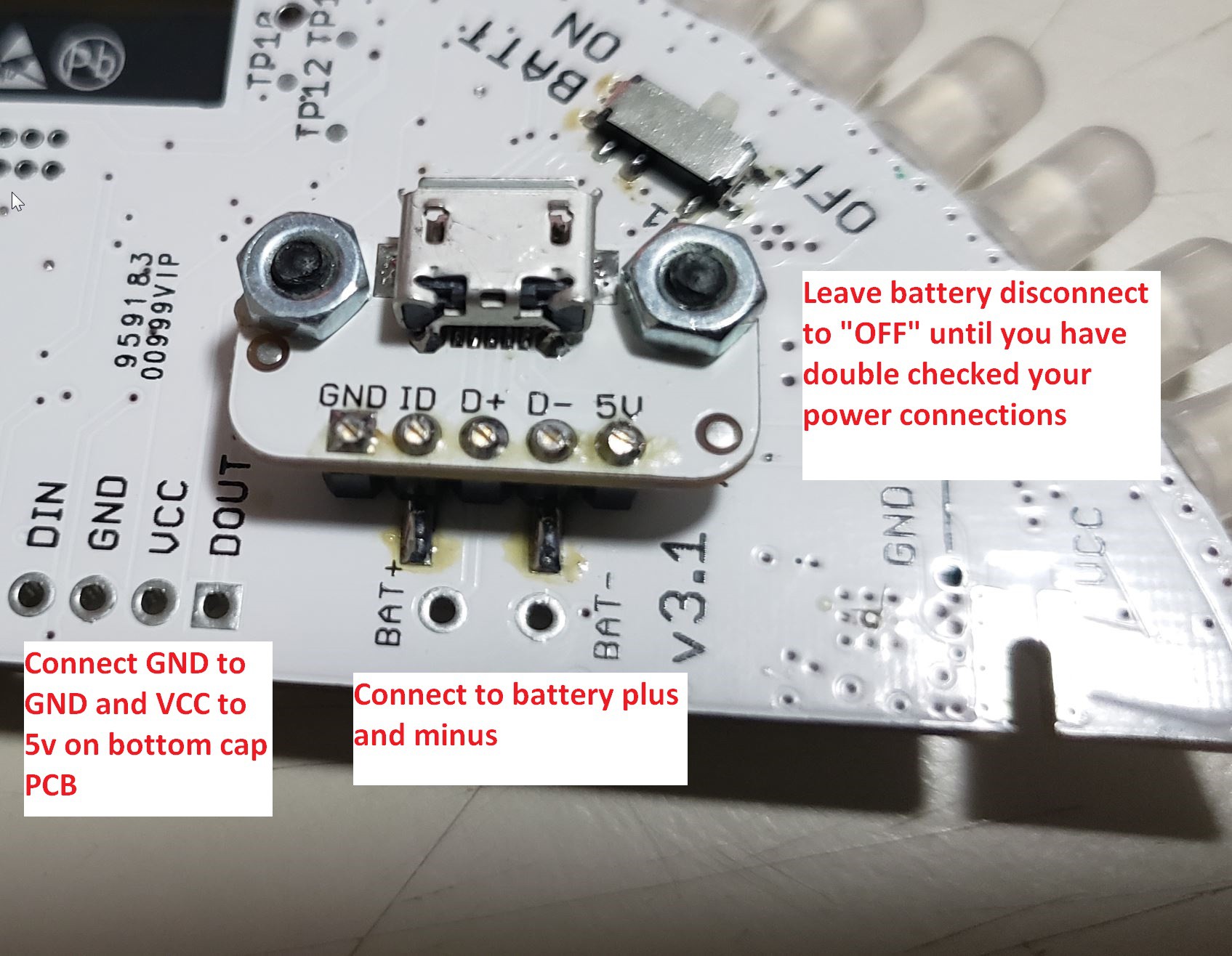
5The battery, 5v and GND
Prep the battery like so:
![]()
And connect to main slice:
![]()
Also connect main slice to bottom cap PCB.
![]()
GND to GND and VCC to 5V
-
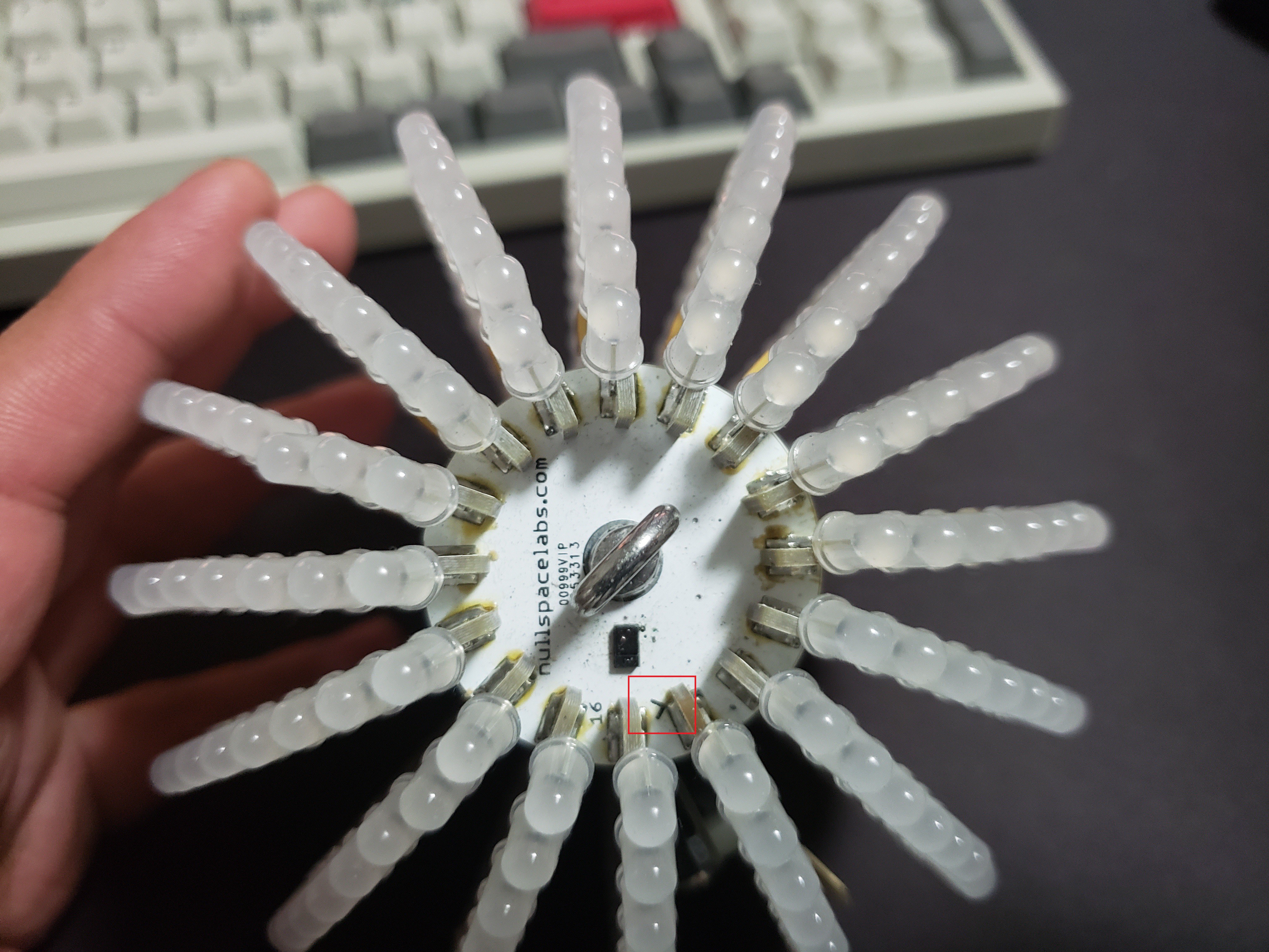
6Final assembly
The main slice needs to be solder to the top cap in a particular slot. It is marked with an ">".
![]()
The slices can be soldered to any slot on the bottom cap.


Discussions
Become a Hackaday.io Member
Create an account to leave a comment. Already have an account? Log In.