-
1▇▇▇▇ Get Familiar with the Simulator ▇▇▇▇
We are going to use an online simulator to develop logic circuits called the Falstad simulator. It is actually very handy as it can simulate lots of different kinds of circuits, but we are only going to use some of its features.
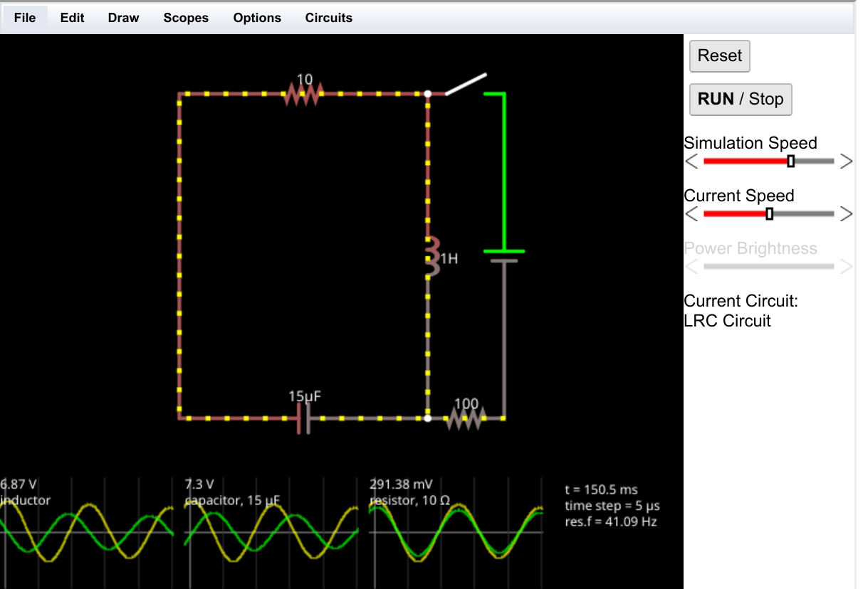
When you go directly to the simulator, you'll see this screen:
![]()
Starting Fresh
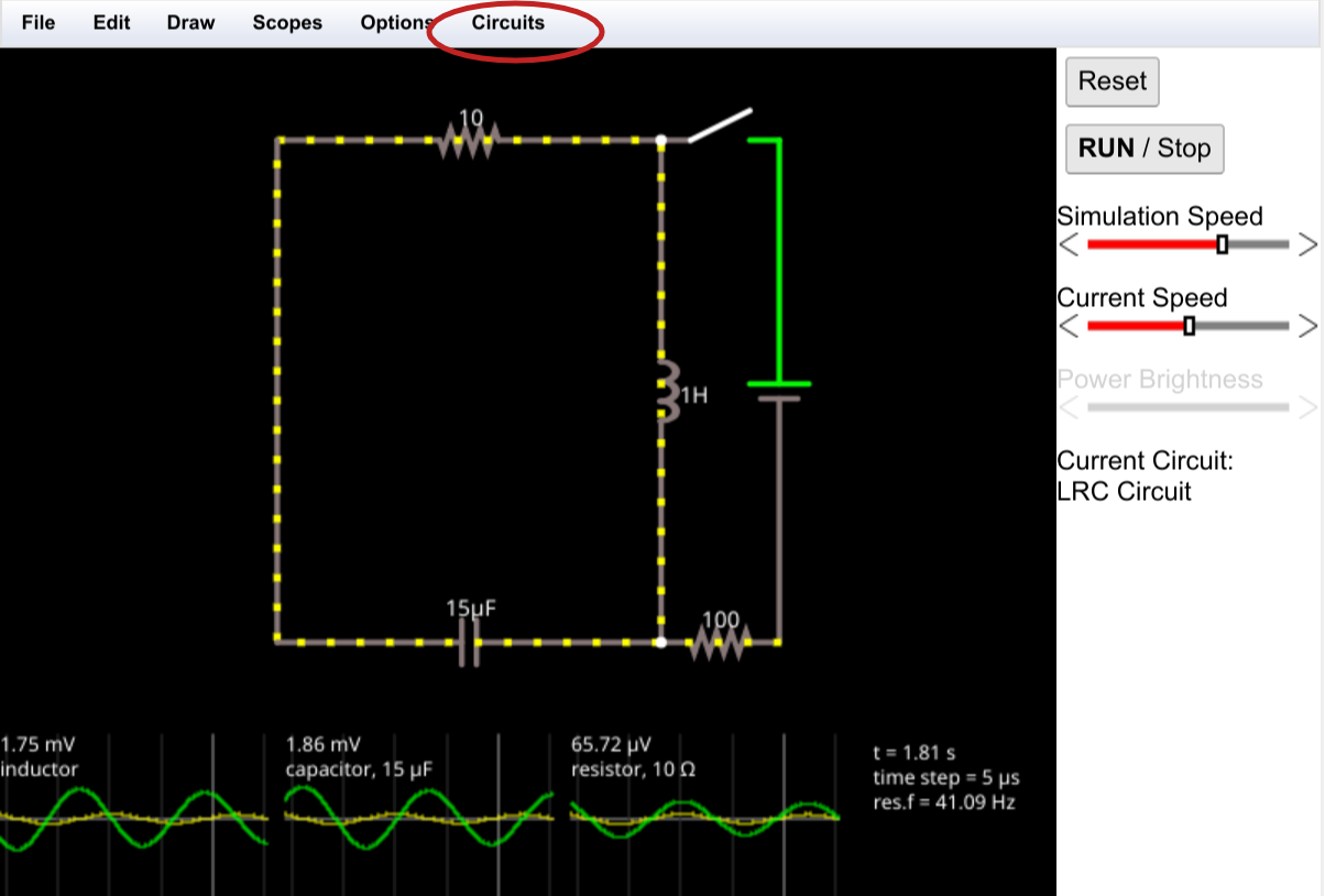
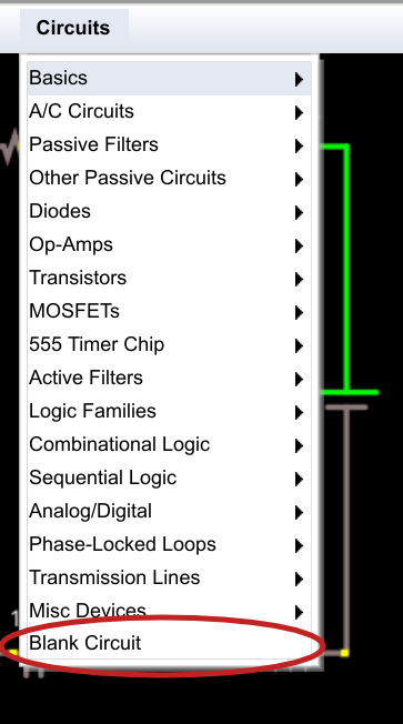
Usually, I'll give you a link to a circuit that's already built. However, it is good to know how to operate the simulator directly. As you can see, there's always a simple analog circuit when you open the page. First thing to do is get rid of it. Click on Circuits and then Blank Circuit.
![]()
![]()
Now you have a blank page to work with. Note how RUN is in upper case and bold?
![]()
That means the circuit is live. If you ever accidentally stop it (the STOP will be upper case and bold) then the circuit won't work until you press run. You might use that button to pause a simulation, but usually just leaving things running is fine.
By the way, if you click on a link to view a simulation I've already set up for you the simulator may show the circuit off to one side of your screen or perhaps even entirely off your screen. To correct this, select Edit | Center Circuit from the simulator's menu.)
Adding I/O
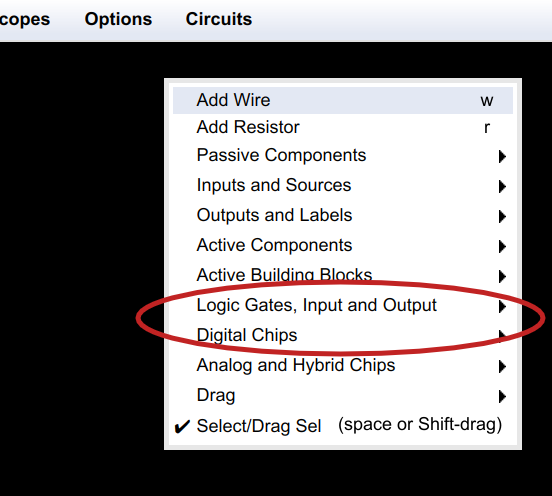
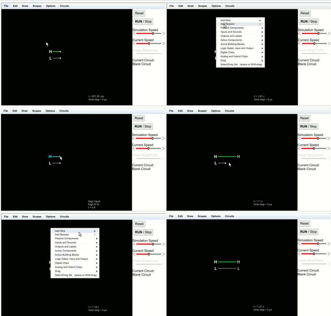
A blank page isn't very interesting. Right click anywhere in the black area (by the way, the Options menu will let you pick a white background if you prefer). You will see a menu appear that will let you pick components to place. We will mostly be interested in Logic Gates, Input and Output along with Digital Chips.
![]()
For now select Logic Gates, Input and Output and pick "Add Logic Input."
![]()
Then use your mouse to click and drag. Where you click will become a terminal and the far end of the drag will say L. Make the length as you please and let go of the mouse button. The whole thing should look something like this:
![]()
The L stands for low which is another way of saying 0 -- one of the two logic states. If you click on the L, it will turn to an H which stands for high -- a logic 1. Each time you click, the input will change from L to H or H to L. In addition -- if you don't change the options -- a wire carrying a high logic level will appear green. A logic low wire will appear gray. Put another input down next to the first one like this:
![]()
You shouldn't have to select the menu again. Just click and drag. You can make as many inputs as you want until you pick another component type from the menu.
You might have noticed on the menu that next to the text "Add Logic Input" there was an "i." That's the keyboard shortcut. The shortcut for "Add Logic Output" is an "o." Try adding two outputs that line up with the inputs. Instead of selecting the menu, just press "o" and then click and drag. But before you do, let's think about where to put them. You'll want to click somewhere near the inputs and then drag away (to the right). See the next section if you want to know where to click or try it and then you can always delete anything you want to change after you read the next section.
Wiring
If you click directly on the terminal, the output will automatically connect to the input. Normally that isn't what you want, but in this case we do. Try drawing one connected output by clicking right on an input terminal and dragging. Then create the second output near the second input but not connected (like in the figure above). Here's what it should look like:
![]()
To connect the input and output terminals you need a wire. You can select "Add Wire" off the right click menu or you can press its shortcut "w." Once you've picked the wire you can click on one terminal and drag to the other.
If you make a mistake, just click on the element you want to remove and use the Delete key. Control+Z will undo your last action, too. The Edit menu has the usual entries like cut and undo, as well.
Once you have connections made, you can click on the inputs and you'll see the corresponding outputs will change. When you make an input H you will see the entire wire will turn green. If not, you probably didn't make the connection the way you thought.
You should wind up with something that looks like this link (the final image in the animation above). Obviously, you might have your positions and lengths a little different and that's OK.
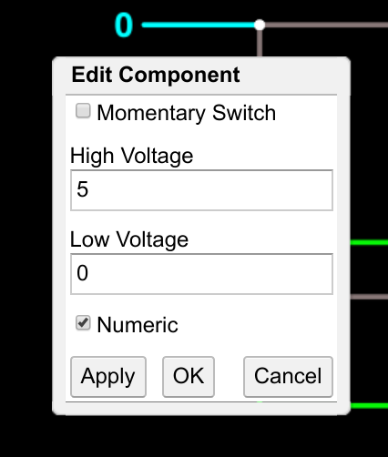
By the way, sometimes you want your diagrams to show 1 and 0 instead of H and L. You can right click on the input and select Edit and check the numeric box if you want that effect. It doesn't change the operation of the circuit, though.
![]()
Next Steps
Having an input tied to an output is not much of a logic circuit! In the next step we will do something more interesting. You can go ahead and select Blank Circuit from the Circuits menu to get ready for that.
By the way, because the simulator totally in your browser, it is hard to save your work. If you look on the File menu, you can see there are several options to export your circuit as a link, in a file, or as text. You can also import text or a file. In the case of the link, just clicking on it loads the circuit which is what I use for the example links in this bootcamp.
-
2▇▇▇▇ Understanding Basic Logic Gates ▇▇▇▇
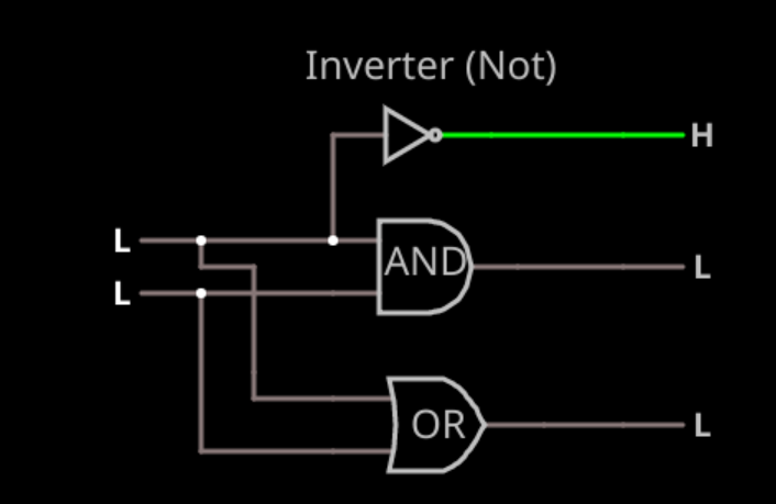
Open the simulator using this link and you'll see the three fundamental logic gates that will build up just about all kinds of logic. To the left are two logic inputs and each gate has its own output. Remember, you can click on the inputs to change from 0 (L) to 1 (H) and see the results.
![]()
You can experiment and find the truth table -- a table that shows the outputs for all possible inputs -- for each gate. I'll call the top input "A" and the bottom input "B":
Inverter:
A Output 0/L 1/H 1/H 0/L The inverter or NOT gate just flips the input to the opposite state.
AND:
A B Output 0 0 0 0 1 0 1 0 0 1 1 1 In English, this gate says that the output will be true (or high) only if A AND B are
both true.
OR:
A B Output 0 0 0 0 1 1 1 0 1 1 1 1 In English, this gate says the output will be true if either A or B is true.
Multiple Inputs
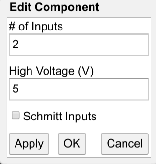
The inverter always has one input, but an AND or OR gate can have as many as you like as long as there are at least two. In the simulator, if you double click a gate that can have more inputs, you will see a dialog that lets you set the number of inputs you want.
![]()
In the case of an AND gate, all inputs -- no matter how many -- have to be high/true/1 for the output to go high. For an OR gate, any input high will set the output, no matter how many inputs there are.
Assertions
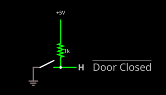
In general, you'll hear people use the words 1 and high used interchangeably to mean a logic 1. However, there is another phrase you'll often hear: asserted. This phrase is a bit tricky. Suppose I have a door open sensor that is a pull up resistor and a normally open switch to ground. When the door is closed, the switch will engage and the output will be low.
![]()
Note the bar over the signal name "Door Closed"? That means the signal is inverted. So a low means the door is closed and a high means it is not. We would often say a signal is "asserted" and in this case that would mean the door IS closed, which is a low. You might also hear the signal is "true" when it it low, although you can't always be sure as sometimes people will say "true" meaning 1.
Notice this is all in how I choose to name things. If I called the signal "Door Open" it wouldn't need a bar and asserted would then be high even though the circuit didn't change at all.
Because it it hard to draw bars over things when typing, you'll sometimes see other ways to indicate a negative true signal:
- a leading slash (/Q)
- a lower-case n prefix or suffix (nQ or Q_n)
- a trailing # (Q#)
- an "_B" or "_L" suffix (Q_B or Q_L)
A Practical Design Experiment
Suppose you had a black box that connected to the door sensor that chimes when the door is open (that is, the sensor output is high). We have a requirement to add a second door. What logic gate would you use to make the chime sound if either door opens?
Your answer should be an OR gate. If either sensor goes high, the output goes high and, thus, the chime sounds.
Now, suppose the black box chimes when the signal is low (that is, the door is closed). We want to chime (low input to black box) if either door is closed). An OR gate won't do it now because the logic is reversed.
The truth table for our function is:
Door 1# Door 2# Chime# 0 0 0 0 1 0 1 0 0 1 1 1 If you look back in the next section, you'll see that this is an AND gate. In fact, for inverted inputs, and AND gate will act like an OR gate and -- you can probably guess -- an OR gate acts like an AND gate.
You don't need to remember the name, but this is Demorgan's theorem. You could have got the same effect by inverting the inputs and then using the gate you'd expect (that is, an OR gate). Then you'd have to invert the output to send to the black box. So now you'd have 4 gates where 1 would do the job.
Minimizing logic like this used to be a big part of digital design. Now (in future bootcamps) we will describe what we want and the computer will figure out the most efficient way to implement it.
-
3▇▇▇▇ More Advanced Logic Gates ▇▇▇▇
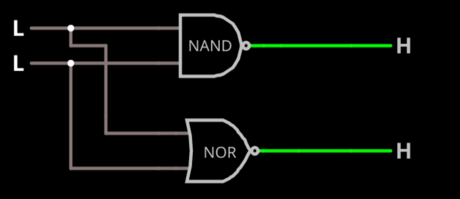
This circuit is similar to the previous one, but it show two new gates: NAND and NOR. These are simply an AND gate and an OR gate with an inverter at the output. So where an AND gate will output a 1, a NAND gate will output a 0. Obviously, you can make these with two gates and the symbol suggests this (an AND or OR gate with a little circle at the output). However, these can often be implemented as a single gate, so it is handy to have symbols for them.
![]()
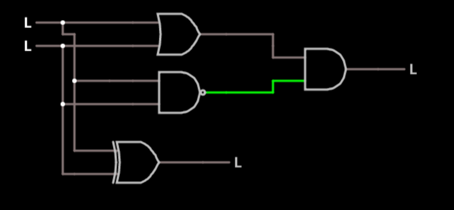
Here's another circuit with a different composite gate.
![]()
See the bottom gate that looks like an OR gate with an extra line? This is a two input gate that has a high output if either input is high, but not both. The three gates at the top (an OR, a NAND, and an AND) implement the same function. That proves that you don't have to have an XOR gate, but it is so useful that it is handy to have a single symbol for it.
This kind of gate is called an exclusive OR or XOR gate. There are two things that make it very useful.
First, look at the XOR truth table:
A B Output 0 0 0 0 1 1 1 0 1 1 1 0 You might make two observations. If A is 0, then the output is a copy of B (or, if you prefer, if B is 0, then the output is a copy of A). But if A is 1, the output is the inverts of B (and the same holds true if B is 1, the output is the inverse of A). This makes the XOR gate a sort of programmable inverter.
The other thing to note is that using binary addition, the output is the sum of A+B. You might wonder how 1+1=0. Well, if you answer is a single bit that's correct, but there is an extra carry bit. This circuit doesn't compute the carry bit, but it does compute the sum. In a future bootcamp, you'll see how the XOR and some other logic can add numbers together in a configuration called a half adder or a full adder.
By the way, the top set of gates is one way to create an XOR gate. You can actually make one using several other methods (for example, using all NAND or NOR gates). So if you see a different schematic for the inside of an XOR gate, that's OK. There's more than one way to do it.
-
4▇▇▇▇ A Decoder ▇▇▇▇
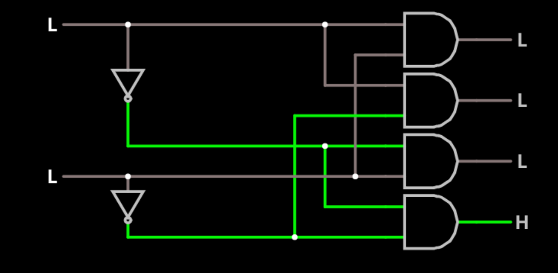
Consider that you have a two digit binary number (which, of course, represents a number between 0 to 3). Perhaps this number indicates the state an automated car wash is in. State 0 is ready, state 1 is washing, state 2 is drying and state 3 is waiting for the clean car to drive away.
You'd like to light an LED for each state so the driver could see a light that says "Drying" or whatever. This is a job for a decoder.
![]()
This might looks a little daunting at first, but it really isn't if you look at it a piece at a time. The first thing to notice is that we have two inverters and two inputs. So we are able to look at an asserted signal if the first digit is high and another asserted signal if the first digit is low.
Let's call the top input digit A and bottom input digit B. The outputs of the inverters, then are A# and B#. The bottom AND gate is the one that will turn on for state 0. That means A=0 and B=0, but it also means A#=1 and B#=1. Therefore, we can use an AND gate with A# and B# to get a high output when the state is 0.
Now look at the next AND gate. It gets A# and B. So it detects 01. It really is that simple.
This kind of logic is known as combinatorial logic. The outputs are purely dependent on the inputs. In other words, suppose the inputs change once per second. You don't need to know anything about this circuit to predict its output other than what the inputs are right now.
This is not always the case. In a sequential circuit, previous states matter. For example, suppose you wanted to build a circuit that counted from 0 to 3, how would you do it? The answer is not like this! But we'll get there using something called a flip flop.
-
5▇▇▇▇ Real World Background ▇▇▇▇
Digital design with combinatorial gates like AND, OR, and NOT gates is relatively straightforward. In particular, when you use these gates to form combinatorial logic, the outputs only depend on the inputs. The previous state of the outputs isn’t important in combinatorial logic. While this is simple, it also prevents you from building things like state machines, counters, and even CPUs.
Circuits that use their own outputs as inputs are known as sequential circuits. It is true that at the fundamental level, sequential circuits use conventional logic gates. However, you usually won’t deal with them as gates, but will deal with abstractions like latches, flip flops, and even higher level constructs. Learning about these higher level constructs will allow you to make more advanced digital designs that are robust. In fact, if you are using an FPGA (the point to these bootcamps), building blocks like flip flops are essential since a large portion of the chip will be made up of some kind of flip flop.
For a better understanding, I want to look at sequential building blocks in two different ways: at the abstraction level and at the gate level. In order to do that, we need to know a little more about how logic gates really work.
Welcome to the Real World
On paper, our circuits are perfect. Wires have no resistance and current flows from one place to another instantly. That’s good for general analysis as real wires have small resistance and the speed of light is usually more or less instant over the distances most of us work with.
However, it is important to realize that these approximations are not how the real world works. In some cases, we’ll exploit the real world effects and in others, we will have to understand them to ensure our circuits work.
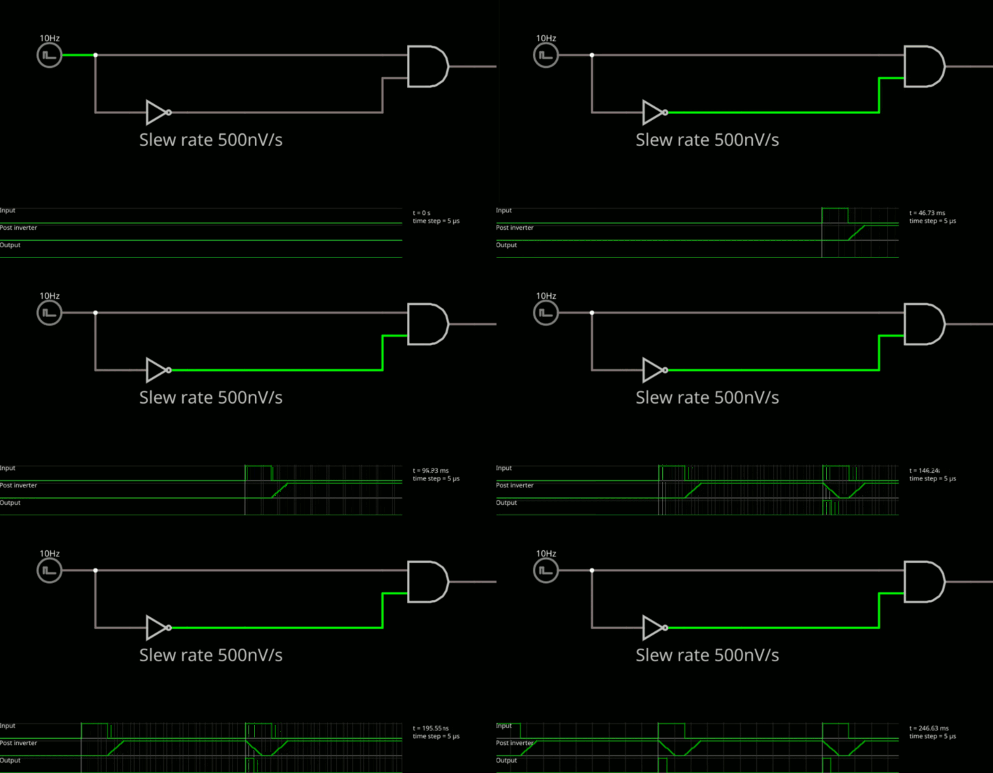
For example, look at the circuit below. What does it do? In theory, it does nothing. An AND gate has to have two true inputs to have a true output and since one input is always the reverse of the other, that can’t happen, right?
![]()
In fact, it can, but only because the circuit elements are not as perfect as we’d wish. When the input to the inverter changes, the output can’t instantly change. Part of that is due to the capacitance of the output circuit. Other delays are due to specific physical effects of whatever element implements the inverter (a transistor, a relay, or a MOSFET, for example).
Consider a time right before the input goes from low to high. The input is low and has been for a long time. The inverter’s output is high, so the AND gate outputs a 0. Now the input goes to the high or true state. The inverter will eventually output a 0, but not right away. Until it does (and assuming the time for the wire to carry the signal change is much smaller than the inverter’s propagation delay) then the AND gate will output a 1 (after, of course, its own propagation delay). This forms a basic rising edge detector. The output pulse’s width will depend on the delay through the inverter. No matter how long the input stays high, there will be just one short pulse at the output.
In real life, you’d want to make the inverter actually quite slow to get a certain pulse width out of the detector and to offset the delay of the AND gate. You might use an RC network to stretch the timing, for example. You could also use an odd number of inverters. If you were designing an IC, you could do things with the device geometry to make it slow.
In the case of the simulator, I set the slew rate of the inverter to 500uV/second. If you visualize the output of the inverter on a scope, you’ll see the output edge is more of a ramp and that is what makes the edge detector work.
Here's what it looks like (the top scope trace is the input, the center trace is the output of the inverter, and the bottom trace is the output of the AND gate):
![]()
-
6▇▇▇▇ The Case for Sequential Logic ▇▇▇▇
It should be pretty obvious that sequential logic is necessary for anything that has memory. However, you’ll find that nearly all real world designs use a specific pattern. Each bit of combinatorial logic will get its inputs from flip flops that use a clock. The outputs will go to other flip flops on the same clock. Those flip flops, in turn, will drive other gate inputs. This is known as synchronous logic.
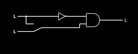
In theory, you don’t have to do it this way. However, if you don’t you are asking for a lot more work. Consider the following scenario. For an industrial control project, you need to quickly shut power down if sensor input “B” goes high unless sensor “A” is also high at the same time. The easiest way to define this is with an AND gate fed with input “B” and the inverse of input “A” (although, of course, there are many ways to do this; that’s not the point).
![]()
Here’s a simulation of the circuit above that also has a slow inverter. If you put the switch in the down position you can control A and B separately. If you throw the switch up, then the top logic input controls both A and B. When A and B go from low to high at the same time, a glitch occurs on the output. If this turned the power off to the machine, it would be an error.
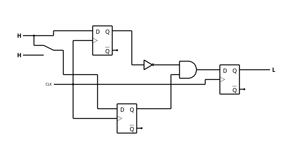
With a clock and flip flops, the slow inverter won’t matter as much. If the longest delay from input to output is shorter than the clock frequency, then the glitch won’t appear on the output. I’ll talk more about a D flip flop later, but for now just think of it is as a one-bit memory. When the clock goes from low to high, the output becomes whatever the D input is at that exact moment. At all other times, the output doesn’t change. Now if A and B are fed into D flip flops and the output goes through a D flip flop, the glitch may still happen, but it will happen while no one is looking (that is, not at a clock edge). it may be true that if a tree falls in an empty forest it still makes a sound, but a glitch that isn’t clocked into a flip flop just disappears.
![]()
Adding flip flops makes the circuit look like the one above. You can see how it works in simulation (again, put the toggle switch up and go from L to H; you’ll see a glitch in the intermediate result, but not on the output).You may notice something. If the input is too short (relative to the clock) the circuit will ignore it. In general, the clock rate needs to be at least twice as fast as the fastest input you need to process.
-
7▇▇▇▇ What's in a Name? ▇▇▇▇
Hopefully by now, you agree that these flip flops and clocked logic are a good thing. There are lots of variations on flip flops and other sequential circuits. However, there are some generally agreed to names that cover the basic types of circuit elements you’ll need. The details, though, may vary (for example, a flip flop might activate on a rising edge of the clock or a falling edge). Other inputs might take a high voltage as a true, while others use a low voltage. The concepts, though, are the same.
In particular, we are going to look at four kinds of flip flops: SR, D, T, and JK. Each of these have different purposes and operate a little differently.
Most flip flops take a clock input and most that you will work with are only sensitive to the edge of the clock. If you think of a flip flop as a memory element, it is going to look at its inputs only at the clock edge, sets its outputs accordingly, and then ignore the inputs at all other times. Some flip flops look at a rising edge (0 to 1) and some a falling edge (1 to 0). A few flip flops don't have a clock at all and others are sensitive to the level of the clock, but those are unusual, especially in FPGAs.
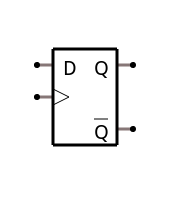
![]()
Regardless of the type of flip flop, there are a few common things to watch for. In a schematic symbol (see above), there will be a small triangle inside the flip flop’s box. This is the clock input. If there is a little circle on the outside of the box right next to the triangle, it is a negative edge or level clock (there isn’t one in the picture on the right). In theory, if the clock has the triangle that means it is only sensitive to an edge, but there are level-sensitive clocks and while it isn't technically correct to put a triangle there, you often see it. Without the circle -- like this one -- it is sensitive to a rising edge.
The output of a flip flop is almost always called Q. As you’ll see, the design usually produces the inverted output for free and that is represented as a Q with a bar over it. In all cases, if the Q output is asserted, the Q-bar (or Q#) output is not and vice versa.
You may find flip flops that have particular features. For example, a preset allows you to force the Q output to true and a reset forces it to false. A synchronous preset or reset only occurs when the clock is active (that is, on the active clock edge or level). An asynchronous preset or reset occurs immediately regardless of the clock. Some flip flops have a clock enable input. When this input is not asserted, the clock is ignored.
In general, you'll find that little circles (like the ones on the output an inverter) on an input indicate an inverted signal. For example, if a flip flop has a RESET pin but it has the little circle, that means that a logic 0 will reset it.
-
8▇▇▇▇ Our First Flip Flop (Sort Of) ▇▇▇▇
Latches have a bad reputation because they are generally not used in FPGA design. At least, not on purpose. Bad coding can produce unexpected latches and these can cause havoc with FPGA tools, especially when they try to make your circuit run at the fastest possible clock speed.
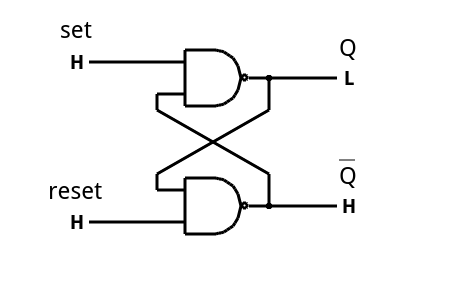
However, latches are an important building block and they are easy enough to understand. The simplest kind of latch is the SR latch (sometimes called an SR flip flop). The S stands for Set and the R stands for Reset. If you assert the S input the Q output will assert. If you assert the R input, the Q output will not assert. If you assert both the S and the R input… don’t do that. The result is undefined, which is one of the problems with using an SR latch.
The logic implementation of an SR latch is simple. It is two inverting dual-input gates (either NAND or NOR) cross connected (see below). Whichever gate you pick, you have to use it for both gates. If you use a NAND gate, the S and R inputs will be active low. If you use a NOR gate, they’ll be active high. The Falstad simulator has an example circuit of a NAND SR latch you can pick from the example circuits menu.
![]()
Improving the Latch
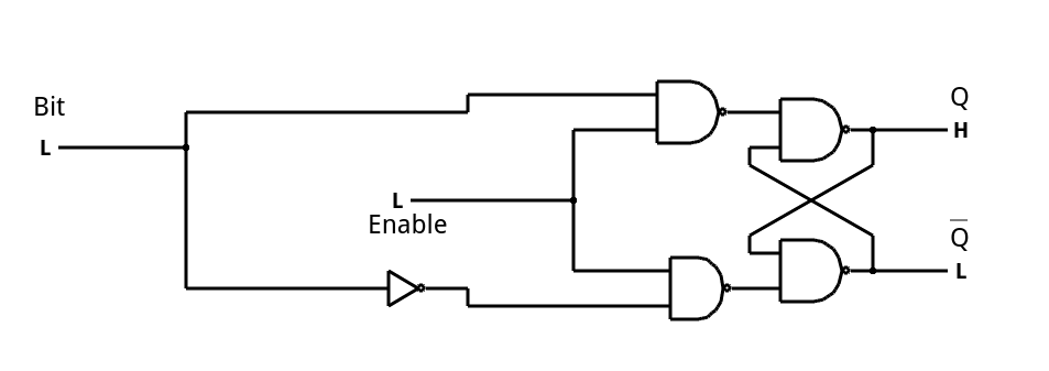
A common enhancement to the SR latch is to include an enable signal. This precludes the output from changing when the enable signal is not asserted. The implementation is simple. You only need to put an additional gate on each input so that the output of the gate can’t assert unless the other input (the enable) is asserted. The schematic appears below.
![]()
In the case of this simulation, the SR inputs become active high because of the inversion in the input NAND gates. If the enable input is low, nothing will change. If it is high, then asserted inputs on the S or R inputs will cause the latch to set or reset. Don’t set both high at the same time when the enable is high (or, go ahead–it is a simulation, so you can’t burn anything up).
That's Memory?
The SR latch could be useful, but in many applications it is inconvenient to have to expressly set and reset it. I said last time, these circuits were like a memory bit, so how could you make the latch just remember the state of a single bit? It’s easy. Just drive the S input with a bit and the R input with the inverse of the same bit. The diagram below is in the simulator.
![]()
This is practically a digital version of a sample and hold circuit. When enable is asserted, the output follows the input. When enable is not asserted, the output holds its value.
-
9▇▇▇▇ D Flip Flops ▇▇▇▇
The SR latch modified with the inverter is often called a D latch because the single input is data for the latch to store. To make it a D flip flop, though, you need to arrange to capture the data at a clock edge, not just any time the latch is enabled.
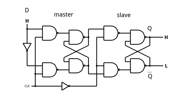
One way this is done is called a master slave flip flop (which doesn’t have to be a D flip flop). The idea is to cascade two latches with a single enable line. However, the first flip flop (the master) gets the enable line straight. The slave gets an inverted copy. What this means is when you enable the flip flop, the master’s output will track the input. However, since the slave is disabled (because of the inverted enable line), no output change will occur. When the enable line drops, the master will hold the last state it saw, but now the slave’s enable line will turn on and the output will change. Since the master’s input can’t change, the effect is the entire flip flop stores the state of the input at the time the enable line is deasserted. Here’s a simulation (see image below).
![]()
It is more common, however, to make flip flops sensitive to the actual clock edge. One simple way to do that would be to use the pulse edge detector we examined earlier to feed the enable output of a conventional latch. The simulator also shows a different method using a few latches, one of which is built with a three-input gate.
In summary, whatever the D input is when the clock edge occurs is what the Q output will be. After the clock edge, it doesn't matter what the D input does, Q will remain the same.
-
10▇▇▇▇ The T and JK Flip Flops ▇▇▇▇
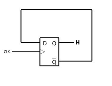
![]()
A T (or toggle) flip flop changes state on each clock pulse (at least, on each enabled clock pulse). This is simple to accomplish if you have a D flip flop. Just connect the inverted Q output to the D input (see left) and you are done. Notice this has the effect of dividing the clock frequency by two, and that’s one thing you frequently use flip flops for: frequency division.
There are many other ways to build a T flip flop, including by wiring the J and K inputs of a JK flip flop together (see below).
JK Flip Flops
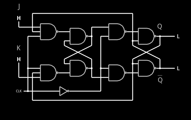
The JK flip flop sounds mysterious, but it really isn’t. Think of it as an SR flip flop where the J input is equivalent to the S and the K input is equivalent to the R. The reason it is not an SR flip flop is that it has well-defined behavior if you assert both inputs at once: the output toggles (like a T flip flop).
![]()
You can find a simulation of the JK flip flop and experiment with it (see image above).
Just to summarize:
J K Q 0 0 No change 1 0 1 0 1 0 1 1 Inverted Q
FPGA Bootcamp #0
If you need a refresher for digital logic before tackling FPGAs, this is the bootcamp for you!
 Al Williams





Discussions
Become a Hackaday.io Member
Create an account to leave a comment. Already have an account? Log In.
Thank you for a great refresher!
Are you sure? yes | no
Thanks for an excellent series !! Note that the link titled "Open the simulator using this link " is broken. The other links work....
Are you sure? yes | no