Close
0%
0%

TERNARO

Open Architecture Ternary FPGA

Public Chat
Similar projects worth following
Balanced Ternary FPGA-like integrated circuit with binary control and open architecture design

TERNARO is planned to be a hybrid integrated circuit working as FPGA-like ternary device with binary control (because nobody invented ternary serial memory yet) that has 9 general purpose ternary IO pins. First prototype of TERNARO in DIP24 package will not be able to read bitstream from external serial memory yet as other FPGAs do. Instead we will need a regular binary microcontroller to feed TERNARO with stream of bits through slave SPI interface to program it after power-on:

         ___________
        /     U     \
 IO1 --|1          24|-- TA0
 IO2 --|2          23|-- TA1
 IO3 --|3          22|-- TA2
 IO4 --|4          21|-- TA3
 IO5 --|5          20|-- TA4
 IO6 --|6  TERNARO 19|-- TA5
 IO7 --|7          18|-- TA6
 IO8 --|8   DIP24  17|-- SDO / TEST
 IO9 --|9          16|-- SDI
Vneg --|10         15|-- SCK
Vref --|11         14|-- /PRG
Vpos --|12         13|-- /RES
        \___________/

Below you can see description of TERNARO pins for that DIP24 package:

pin 1 - IO1 (general purpose ternary IO)
pin 2 - IO2 (general purpose ternary IO)
pin 3 - IO3 (general purpose ternary IO)
pin 4 - IO4 (general purpose ternary IO)
pin 5 - IO5 (general purpose ternary IO)
pin 6 - IO6 (general purpose ternary IO)
pin 7 - IO7 (general purpose ternary IO)
pin 8 - IO8 (general purpose ternary IO)
pin 9 - IO9 (general purpose ternary IO)
pin 10 - Vneg (common ground connected to chip substrate)
pin 11 - Vref (intermediate voltage level between Vneg and Vpos)
pin 12 - Vpos (common power +5V)
pin 13- /RES (reset of Slave SPI and clear configuration memory)
pin 14 - /PRG (programming enabled through Slave SPI)
pin 15 - SCK (input clock for Slave SPI)
pin 16 - SDI (serial data input for Slave SPI)
pin 17 - SDO (serial data output from Slave SPI if TA=0) or TEST
pin 18 - TA6 (test address bit 6)
pin 19 - TA5 (test address bit 5)
pin 20 - TA4 (test address bit 4)
pin 21 - TA3 (test address bit 3)
pin 22 - TA2 (test address bit 2)
pin 23 - TA1 (test address bit 1)
pin 24 - TA0 (test address bit 0)

Chip will allow to read up to 128 internal ternary points for debug purposes (testing point is chosen by TA0...TA6 address bits) that is connected to TEST output (which is used as SDO if all TA bits are grounded).

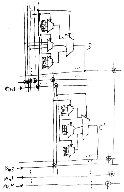
Internally TERNARO will have 7x9 grid of ternary configurable logic blocks as one showed below:

Analog interconnect will electrically connect every vertical line to nothing or only one horizontal line (line 15 is an external pin and lines from 1 to 14 are connected to 7 logic blocks in that row):

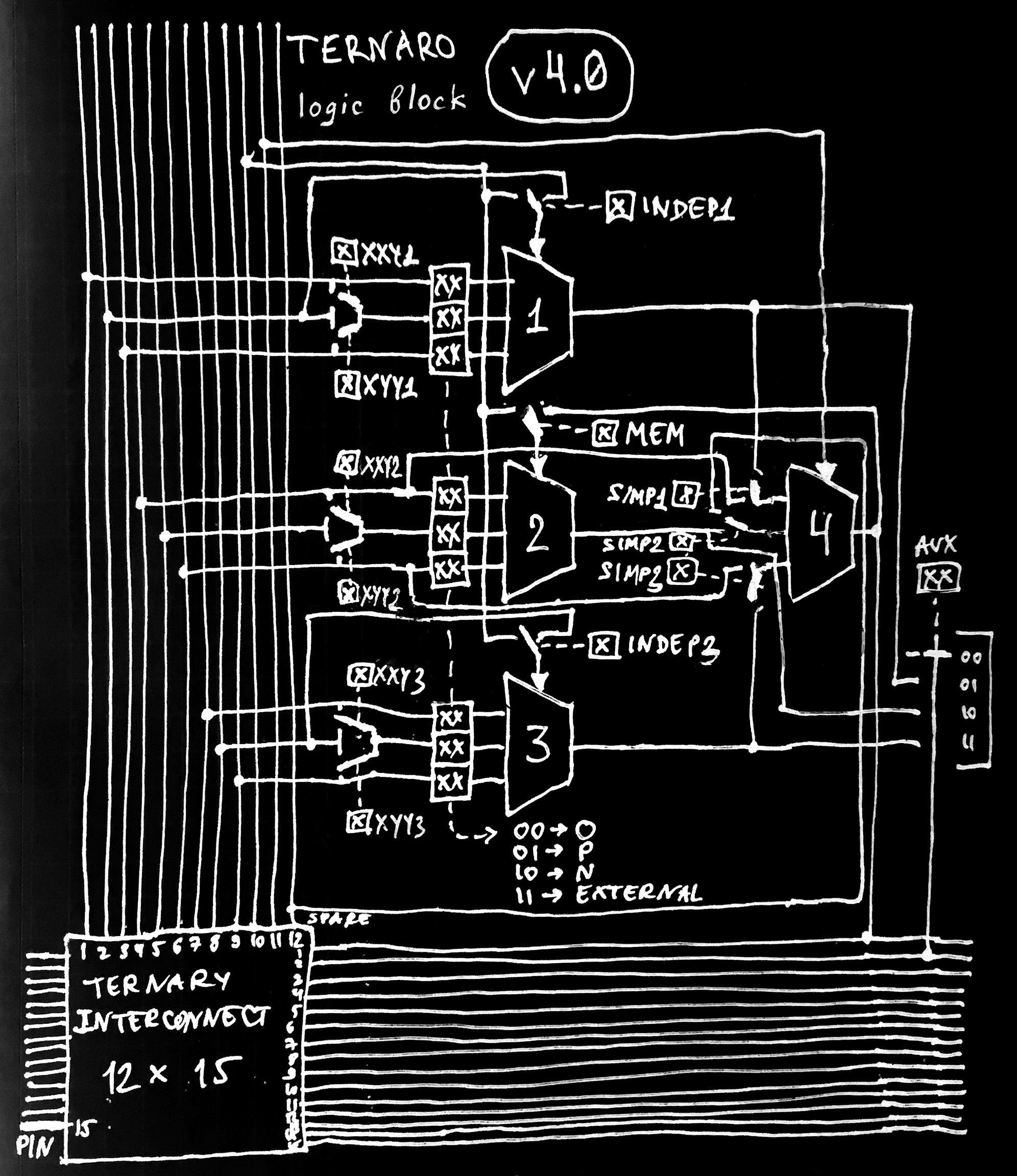
Every such interconnection block will be configured by 6 bytes (every 4 bits say where every vertical must be electrically connected in the channel while 0000 will mean no connection) and every logic block is configured by 4 bytes:

Byte 0 - 1st selector:
 bit 0 - input N of 1st selector
 bit 1 /
 bit 2 - input O of 1st selector
 bit 3 /
 bit 4 - input P of 1st selector
 bit 5 /
 bit 6 - make 1st selector E21 (XXY1)
 bit 7 - make 1st selector E12 (XYY1)

Byte 1 - 2nd selector:
 bit 0 - input N of 2nd selector
 bit 1 /
 bit 2 - input O of 2nd selector
 bit 3 /
 bit 4 - input P of 2nd selector
 bit 5 /
 bit 6 - make 2nd selector E21 (XXY2)
 bit 7 - make 2nd selector E12 (XYY2)

Byte 2 - 3rd selector:
 bit 0 - input N of 3rd selector
 bit 1 /
 bit 2 - input O of 3rd selector
 bit 3 /
 bit 4 - input P of 3rd selector
 bit 5 /
 bit 6 - make 3rd selector E21 (XXY3)
 bit 7 - make 3rd selector E12 (XYY3)

Byte 3 - additional configuration:
 bit 0 - connect feedback line to form MEM block
 bit 1 - simplification bit SIMP1
 bit 2 - simplification bit SIMP2 (spare input control)
 bit 3 - simplification bit SIMP3
 bit 4 - make 1st selector independent (INDEP1) 
 bit 5 - make 3rd selector independent (INDEP3)
 bit 6 - AUX line control (see below)
 bit 7 /

AUX line control configuration:
00 - not connected
01 - 1st selector output
10 - 2nd selector output
11 - 3rd selector output

Input configuration for selectors (bits 0...5 of first 3 bytes):
00 - constant O (neutral)
01 - constant P (positive)
10 - constant N (negative)
11 - through signal

Note: XXY and XYY...

Read more »

  • TERNARO playground

    SHAOS08/10/2018 at 08:23 0 comments

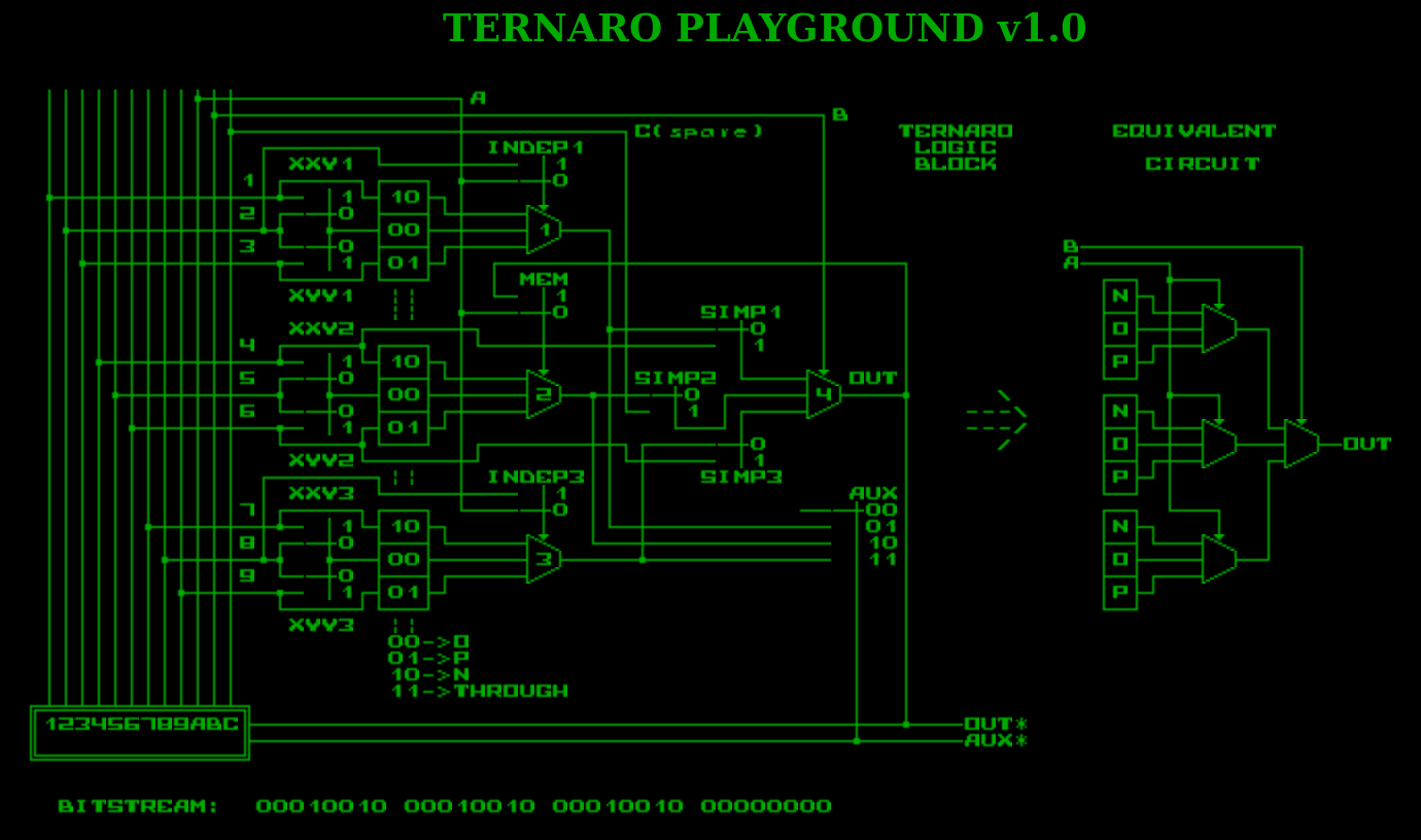
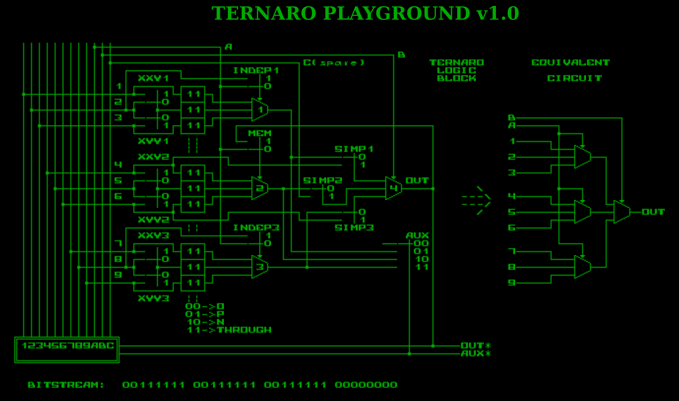
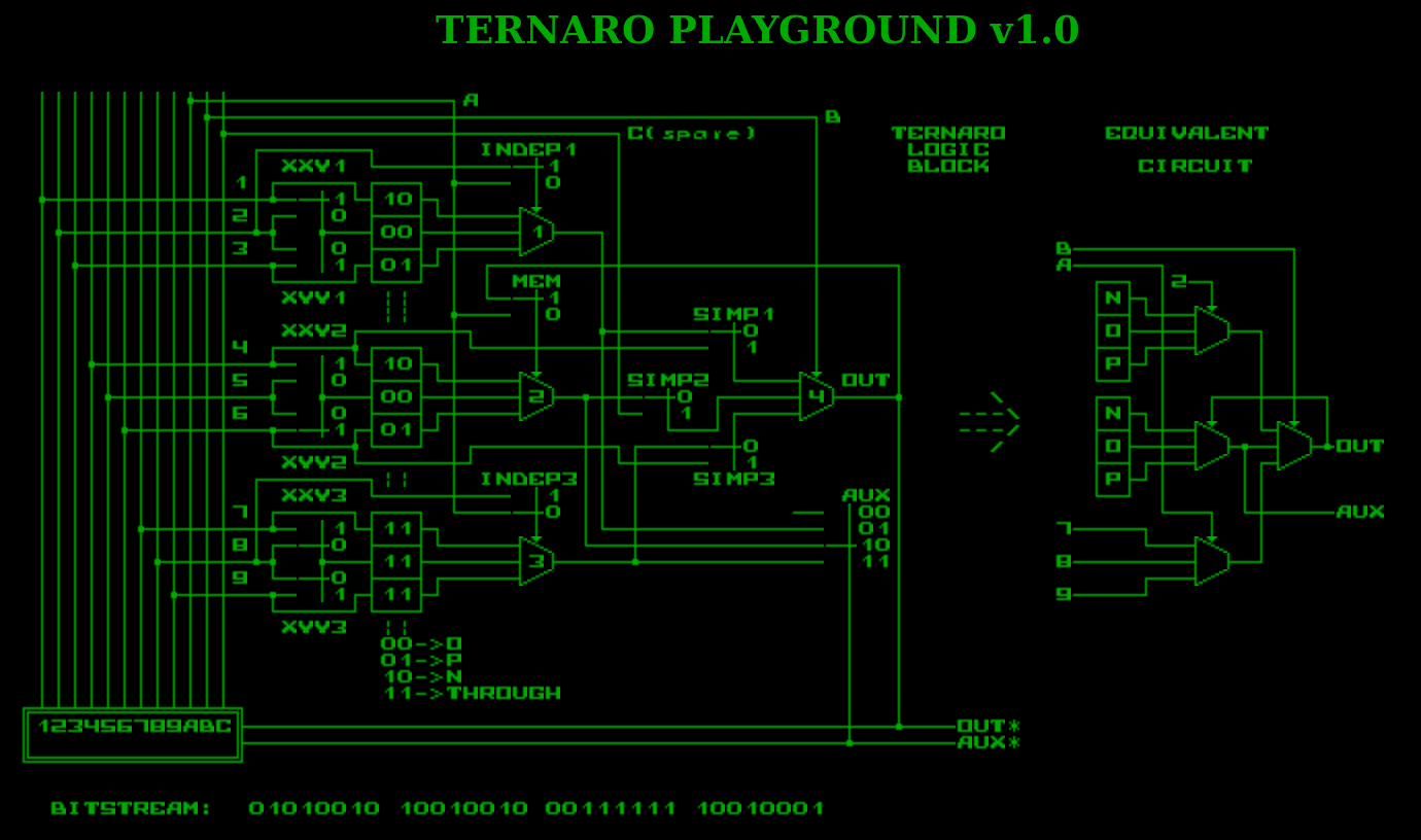
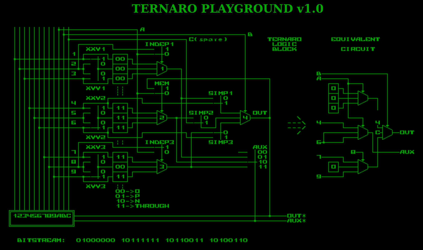
    Using Circuits.CC engine I created an interactive web site TERNARO.COM where you can play with different switches of TERNARO configurable logic block (by mouse) and see how they are translated into bitstream (at the bottom) and how equivalent circuit may look (on the right) - this should help other people to understand how it's supposed to work...

    For example, this is 2-input LUT (can be used as 9-trit ROM):

    This is 9-to-1 multiplexer:

    Memory (transparent latch) with 2 independent inputs (2nd MUX must be in buffer mode NOP):

    And it could be any mix of the settings:

    Enjoy ;)

    P.S. Source code to look at: https://gitlab.com/shaos/circuits_cc/blob/master/src/TERNARO.R

    and https://gitlab.com/shaos/circuits_cc/blob/master/www/ternaro.html

  • Binarized TERNARO

    SHAOS07/29/2018 at 10:15 0 comments

    Yes, ternary FPGA could be used as binary FPGA :)

    In case of TERNARO for this purpose every 3-input ternary multiplexer should be converted to 2-input binary multiplexer by setting XYY or XXY configuration bit  - it turns every MUX to E12 or E21 respectively:

    From binary point of view E12 is a multiplexer with lower threshold (about 2.1V for 5V power supply) and E21 is a multiplexer with higher threshold (about 3.5V for 5V power supply). So now we can build circuits with hysteresis (see this log for more info about actual thresholds):

    Also in case of "binary mode" multiplexer 2 will be used only to form MEM cell (and will be ignored if logic block is used as LUT), so vertical signals 4,5,6 will be always free to be used for interconnect.

    Another interesting trick - in "ternary mode" every constant O (set by 00 pair) is actually direct connect to input Vref, so in "binary mode" we may re-name input Vref to I0, because effectively it becomes additional general purpose input for the circuit (input number zero). And constants N and P in "binary mode" becomes "0" and "1" respectively (as they stay to be direct connects to ground and positive power supply):

    00 -> Vref input of the chip (I0)
    01 -> Constant "1"
    10 -> Constant "0"
    11 -> Through connection to vertical line

    Later we can add support of "binarized TERNARO" into Yosys for example and then people will be able to program TERNARO using standard Verilog :)

  • TERNARO topology

    SHAOS07/27/2018 at 05:13 0 comments

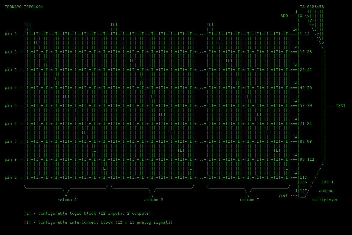
    This is how I imagined TERNARO from inside:

    Bitstream should define every column one by one (from left to right) with every channel in the column (from top to bottom) like L-I-I-I-I-I-I-I-I-I (4+6*9=58 bytes per every channel/column intersection).

    Every interconnection block [I] behaves as 12 switches with 16 positions each (position #0 means no connection):

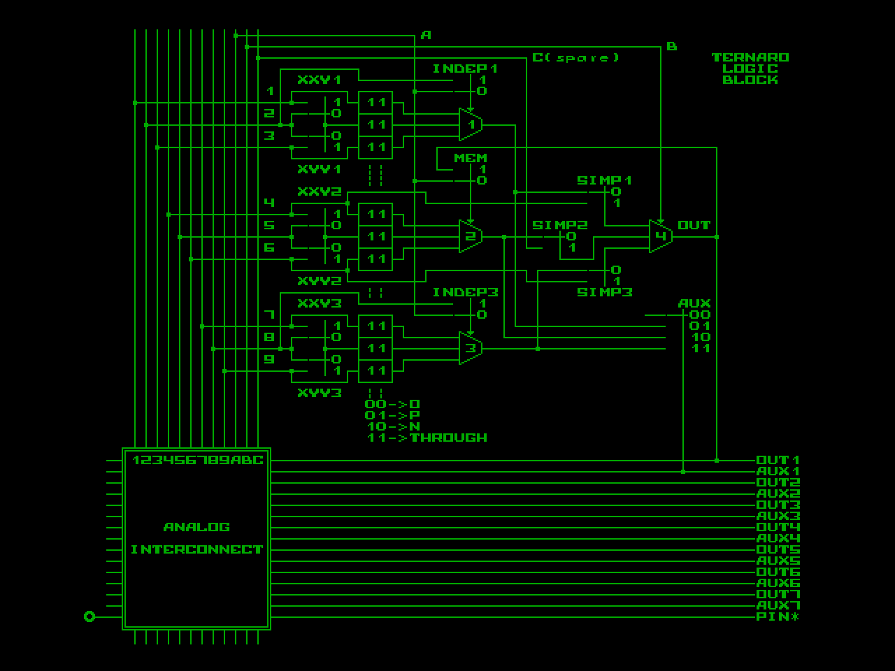
    And every logic block [L] looks like this (with nearest interconnect showed as well):

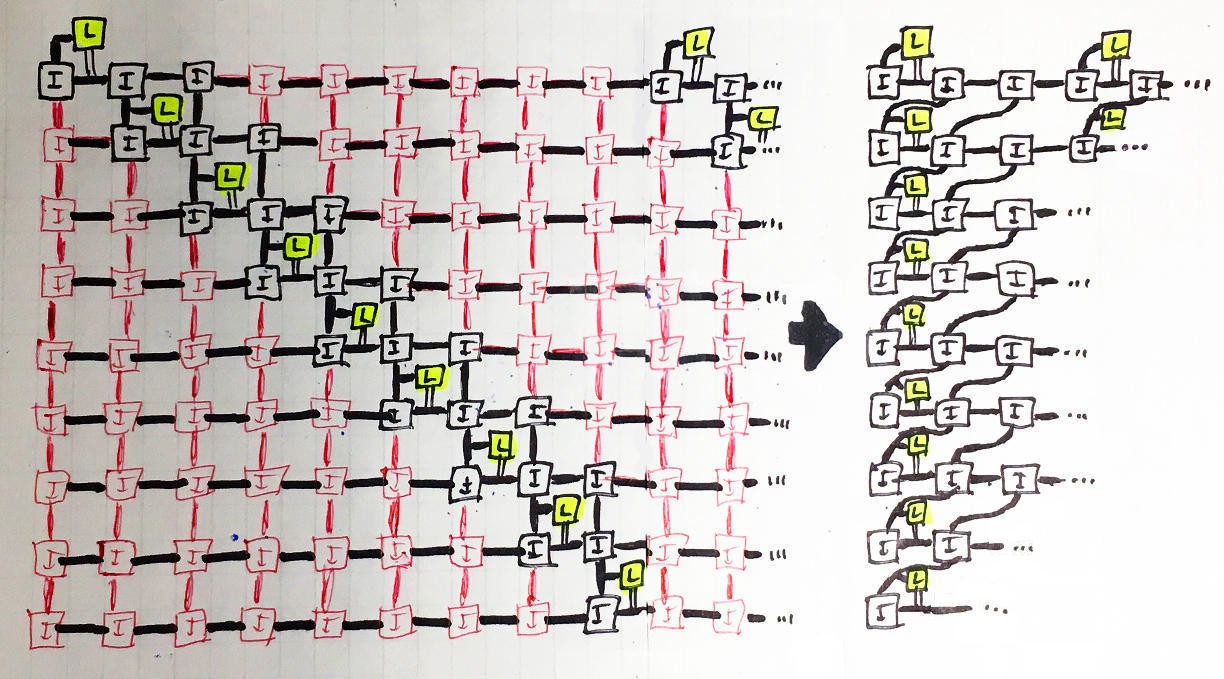
    Approach when adding another pin (and another horizontal channel) requires additional interconnect block in every channel for every column is not very scalable. So later I can do some reduction like showed below:

    In this case it will scale linearly with adding more pins. How many diagonals with interconnects can be removed to still be flexible for most real life applications? Honestly I don't know. Probably I need to write synthesis/place&route software first and see how it goes with different numbers. This is how one of the most extreme cases of reduction can look:

  • Bigger picture

    SHAOS07/22/2018 at 09:59 0 comments

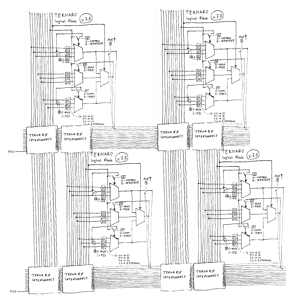
    As I wrote before it should be a grid of 7 x 9 logic blocks (63 total) where every horizontal "channel" is having 15 lines and one of which is a pin (so it is 9 pins total), but less number of channels is also possible - for example below is 2 x 2 (unpractical because of only 2 IO pins are there, but good enough for demonstration purposes): 

    So in case of full scale 9 channels (one horizontal channel per every IO pin) every TERNARO logic block will need NINE interconnect blocks to cross every channel, so total length of bitstream will be (4+9*6)*63 = 3654 bytes (from up to down from left to right) and this bitstream needs to be pushed into the chip by external microcontroller (binary one of course).

    About testability - test address inputs TA0...TA6 (address is binary) will choose which HORIZONTAL ternary line needs to be connected to test output TEST - it is 15*9=135 of them, but as we can see every 15th one is an IO pin, so we obviously have direct access to pins already and we can skip all of them so it's 135-9=126 total plus 1 output for SDO - serial data out for Slave SPI - if TA=0:

    0000000 (0)  - SDO output of Slave SPI
    0000001 (1)  - signal 1 of 1st channel
    0000010 (2)  - signal 2 of 1st channel
    0000011 (3)  - signal 3 of 1st channel
    0000100 (4)  - signal 4 of 1st channel
    0000101 (5)  - signal 5 of 1st channel
    0000110 (6)  - signal 6 of 1st channel
    0000111 (7)  - signal 7 of 1st channel
    0001000 (8)  - signal 8 of 1st channel
    0001001 (9)  - signal 9 of 1st channel
    0001010 (10) - signal 10 of 1st channel
    0001011 (11) - signal 11 of 1st channel
    0001100 (12) - signal 12 of 1st channel
    0001101 (13) - signal 13 of 1st channel
    0001110 (14) - signal 14 of 1st channel
    0001111 (15) - signal 1 of 2nd channel
    0010000 (16) - signal 2 of 2nd channel
    .....
    1111110 (126) - signal 14 of 9th channel
    1111111 (127) - Vref (for testing purposes)

    And we have 1 extra signal (when TA=127) that could be used for example to test internal Vref level...

  • Logic behind TERNARO

    SHAOS07/22/2018 at 00:14 0 comments

    I'm working on TERNARO design since January 2015. Main idea was to design ternary FPGA that may implement any ternary circuit that is built out of bunch of TRIMUXes (like TRIADOR from #Homebrew ternary computer for example). Base element of such FPGA that was chosen in 2015 is 9-to-1 ternary multiplexer:

    It also may be used as 9-cell ternary ROM with 2-trit address and 1-trit output.

    With little re-wiring we can get memory element out of it:

    Left-center ternary multiplexer is connected as a buffer (unary function NOP) and it's the main reason why it becomes a memory cell with feedback loop like that.

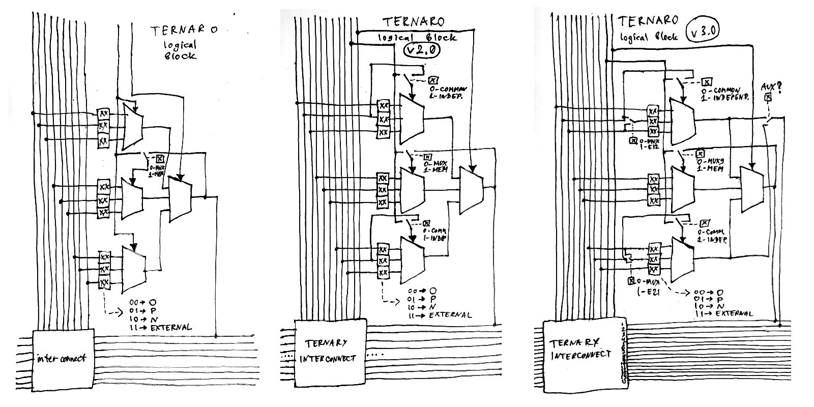
    This is all versions of TERNARO configurable logic block design that I came up with in the last few days and you can see how it evolved in my mind :)

    Today version 4 is the last and final design:

    Now 9-to-1 multiplexer may be split to separate 3-to-1 multiplexers. But even with initial programmable capabilities we can easily implement things as ternary half-adder for example:

    Also if we have 9 IO pins it means we have 9 horizontal channels with 15 signals in each...

View all 5 project logs

Enjoy this project?

Share

Discussions

Dasein Adams wrote 12/03/2022 at 14:06 point

Any new updates on the project as we head into 2023? 

Have been trying to find out if there was anything experimental like this project for a while :3 

  Are you sure? yes | no

SHAOS wrote 05/28/2023 at 09:21 point

No updates yet

Currently playing with TinyTapeout and efabless experimental GF180 free shuttle to use in future for actual chip :)

  Are you sure? yes | no

claudio.larosa74 wrote 01/09/2019 at 16:27 point

Congratulations on this project!

I have a question: did you already have the chip fabricated?

How is it possible to build a chip?

  Are you sure? yes | no

SHAOS wrote 01/11/2019 at 05:39 point

No, I didn't have actual chip yet

If I find funds I'll use the same approach as I did in 2015:
https://hackaday.io/project/11779-shared-silicon

But for now it's more important to create simulator and tools to prove that this FPGA design is having any sense

  Are you sure? yes | no

SHAOS wrote 07/29/2018 at 03:36 point

Today I moved from DIP24 to DIP28, but to keep design consistent I have only 24 pins useful, so 4 new pins are N.C. (not connected)

  Are you sure? yes | no

Similar Projects

Does this project spark your interest?

Become a member to follow this project and never miss any updates