Close
0%
0%

Gamma PIN - Semiconductor Radiation Detector

An attempt to design and deliver universal and accessible radiaton analyser to be used in nuclear spectroscopy

Similar projects worth following
All the time we are exposed to various kinds of radiation. The one that we are least aware
of is the ionizing radiation and elementary particles associated with it. They pass through objects and our body leaving a trail of ions in their path and inducing changes.
Energies of those corpuscles change as they travel through distinct environments.
Having the ability to measure energy of each particle enables us to identify it's source whether
it is terrestrial - coming from some mineral or extraterrestrial like a cosmic ray hurtling through space.

A good radiation analyzer should be able to measure the energy of each quant,
it's trajectory, overall dose of radiation and energy spectrum of the source.
This research project is aimed at achieving and evaluating best results with accessible components. Based on the experience of previous designs and promising simulations
I hope to optimize the prototype version to use it for amateur nuclear spectroscopy.

The physical basis of capturing the ionizing radiation’s energy:

Ionizing radiation is a broad term for all the particles and quants that are capable of knocking away electrons from shells of atoms an molecules. There are a few of classified ionizing corpuscules and quants like:

  • α - alpha particle which is doubly ionized atom of helium
  • β - beta particle that may be an electron β or positron β+
  • γ - gamma radiation consisting of quants that are high energy photons.

There are more particles that are capable of ionizing matter by various interactions: muons, neutrons, protons but for the early stage of the research I would like to focus on the most common ones.

All those particles and quants carry energy, which is receding as they move through matter. This overall energy is lost due to various collisions and affections. As a result ions and electrons are liberated, which form tiny electric charge. The amount of the charge is directly proportional to energy of the particle to some extent.

Under special conditions this residue of charge left after passing of a particle may be collected and applied to estimate the energy and trajectory of it. The only thing required to do this is to measure the generated charge or current and analyse the results.

In this research project the medium to measure the radiation particles will be PIN diode. It is a flat slice of 3 semiconducting materials. Following the order P – positivly doped,  I- intrinsic (undoped) and N – negatively doped semiconductor. When the energetic particle or quant strikes the I – undoped region, it easily conveys the energy to the silicon atoms creating electrons and holes. Those two opposite kinds of charged particles then are attracted by the electric field coming from the biasing voltage applied to the diode.

As those opposing clouds of charge are separated a pulse of current occurs, which can be measured using ultra low noise and precise amplifier circuits.

Drawing illustrating pair generation in the semiconductor

The circuitry:

The whole instrument will be consisting of a few functional blocks, which will be tested and designed individually, but with consistency to provide high end results.                    
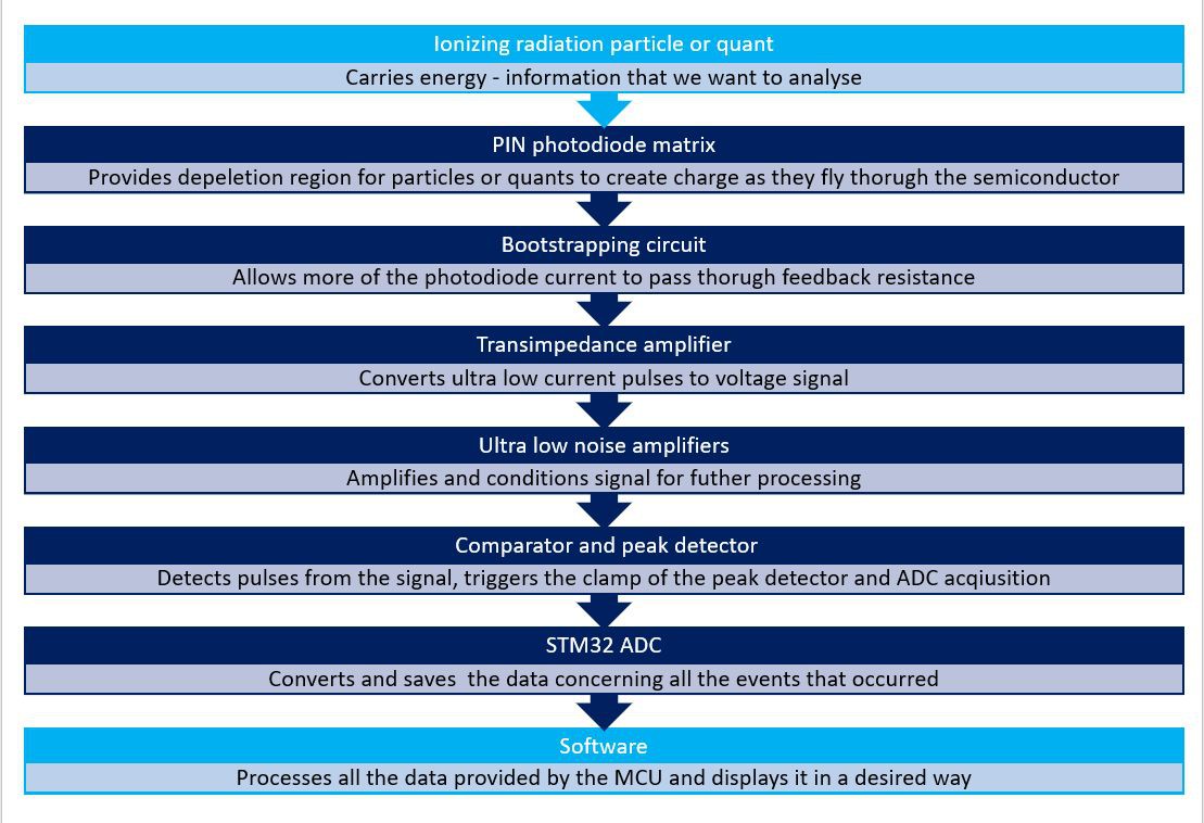
Graph describing the flow of information thorugh the device.

  • Sensing matrix – in the first stage it will consist of an array of common BPW34 PIN diodes. As the project develops I will test some larger ones I found on the Internet under the misterious name 2DU10 (10x10mm). If those common diodes fail to meet the expectations I may even move to professional detectors produced by First Sensor or photo multiplier diodes or replace the semiconducting area with a high voltage PMT and a chunk of scintillator.
  • Booststrapping circuit – while using larger diodes, their capacitance significantly reduces the charge generated by each event. There is a proposed solution that can be found on the website of Analog Devices. The simulations conducted for the detector in LTspice confirm the utility of this simple circuit, which will enable to use greater sensing areas.
  • Transimpedance amplifier – the heart of the detector, the task of it is to make the awfully little current pulses noticeable for the following parts. It needs to be as sensitive, wideband and low noise as possible. There are only a few of such amplifiers, with ultra low biasing current suitable for the job, like LTC6268 or LMP7721. I will test them both, because I couldn’t decide which one is better. The second most important part of this circuit – the feedback resistor will be chosen basing on the simulations concerning the signal to noise ratio.

  • Ultra low noise amplifiers – the small singal needs to be processed and conditioned for the acquisition. It will be achieved using LT6232 – a quad ultra low noise and wideband amplifier. The three of the amplifiers will be working in a inverting mode each stage with aproximate amplification of 10x. The last stage will be a substractor without amplfication to separate the signal from the noise. The value of substraction will be set by a digital potentiometer. In the future expansion of the detector the working points of each module will set similary.

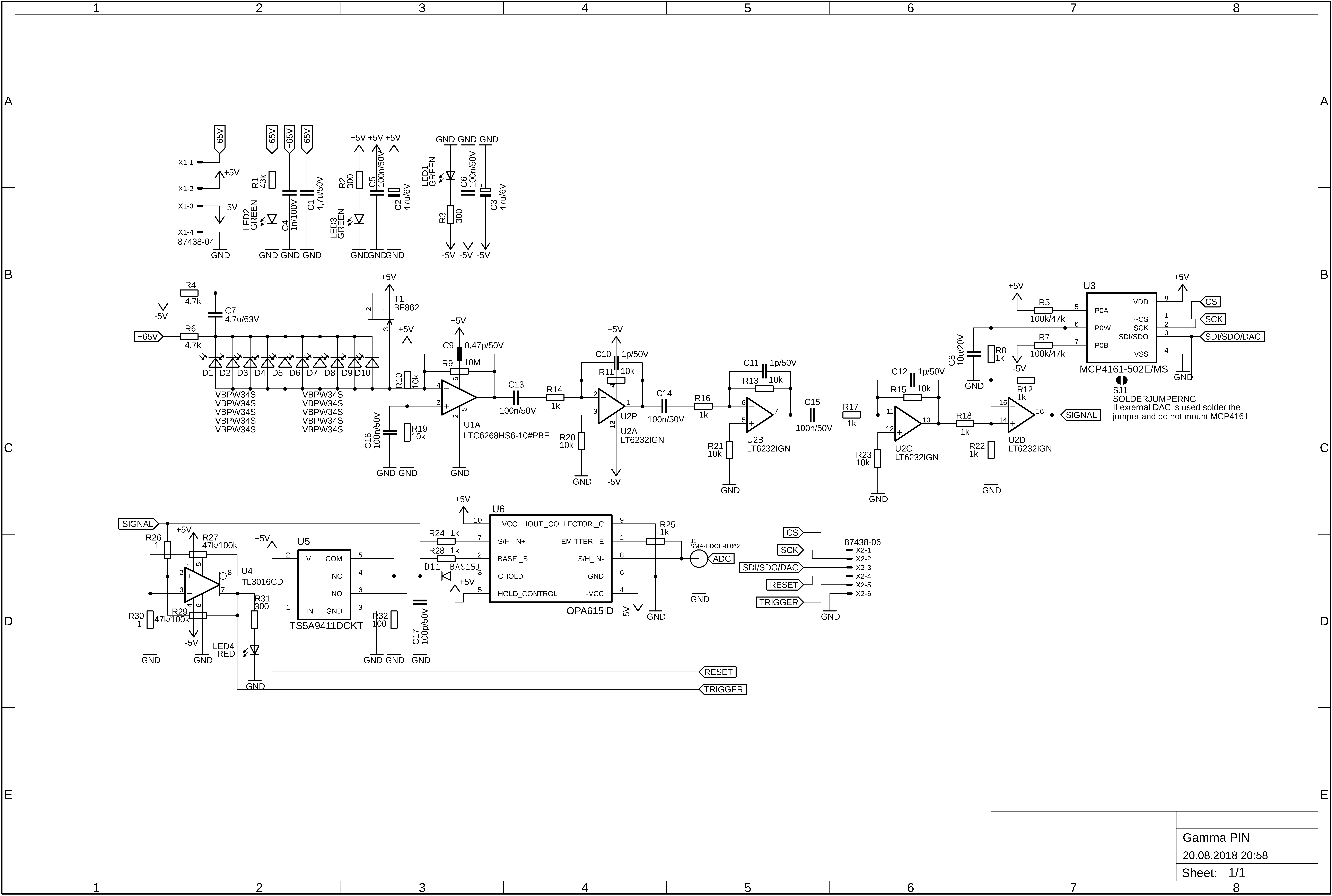
  • Comparator and peak detector – a positive signal sensing ultra fast comparator TL3016 will send  a signal, that a pulse has been detected to the STM32. The MCU will manage the clamp of the extremely fast single peak value detector based on OPA615 with a resetter switch of TS5A9411. After the pulse is detected the clamp will last for the detector to charge the capacitor to the highes value of the pulse. After a while when the value is settled the STM32 ADC will sample and save it. This mechanism will be perfected on the working circuit.

  • STM32 MCU – for the sampling and processing the data I have chosen NUCLEO-H743ZI, that should easily manage all the tasks with sufficient resolution. With 3 ADCs that can provide up to 16 bits of resolution with a high sample rate (up to 36 channels, 4.5 MSPS at 12 bits) it should be more than enough for this application.

  • Software – all the data will be send over the serial port or saved on the SD card. Having finished the instument, the extensive analysis of the collected data may begin. Starting from the nuclear spectroscopy, particle tracking, environment monitoring to gathering the data for educational use.
Read more »

  • 10 × BPW34S/TEMD5010X01 Opto and Fiber Optic Semiconductors and ICs / Photodiodes
  • 1 × BF862 Discrete Semiconductors / Transistors, MOSFETs, FETs, IGBTs
  • 1 × LTC6268/LTC6268-10 Current FET Input Op Amp
  • 1 × LT6232 Ultra Low Noise Rail-to-Rail Wideband Op Amp
  • 1 × MCP4561-502 Data Converters / Digital Potentiometers

View all 10 components

  • Assembly and tests of the third prototype

    Marcin Wachowiak03/01/2020 at 17:56 0 comments

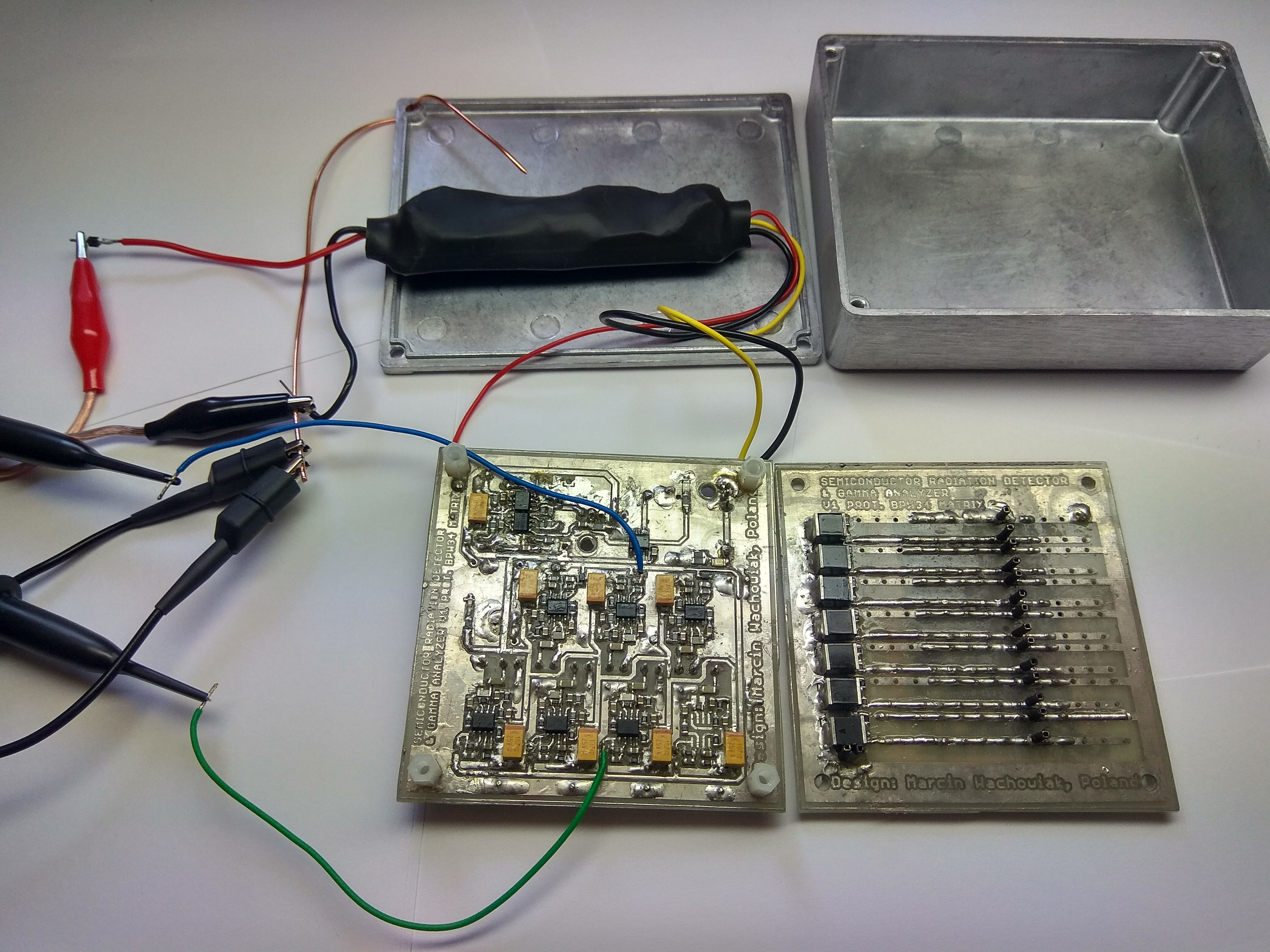
    Recently I found a while to solder and test the latest prototype. All boards have been soldered using a hotplate made from an old iron. The soldering process took about 1 minute, because the iron didn't have a temperature controller to follow the reflow profile. The only thing that prevented burning the boards was a thermostat set around 230 °C. I hope to add a controller soon to improve the performance. There are a few neat controllers on the Internet, this one seems suitable for my needs - https://github.com/makermoekoe/Hotplate-Soldering-Iron

    Assembled prototype

    Preamplifier

    As you can see, I produced two versions of the preamplifier: one with a single diode and another with a full array of 10. The following results have been obtained using the single diode version as it is less noisy.

    The boards turned out to have some flaws but still I managed to get them to work properly.

    Issues with the preamplifier board:

    • Guard ring introduced to reduce current leaks emerged to be a source of shorting. Exposed traces with components placed upon them were not a good idea. Covering the guard ring with solder mask would render it useless as it is supposed to prevent any currents flowing through surface form contaminations by shunting them to low-impedance node. (topic about it) I may consider to expose only thin edges of the trace and cover the wider areas susceptible to shorting. For the time being I have milled it out to get a functional circuit.
    • The second op amp used on the board as subtractor with amplification requires a feedback capacitor to ensure the stability and prevent excitation. It should be around 22-33pF and can be simply placed on the top of the feedback resistor - R17.
    • Voltage reference for the subtractor had to be altered to set the output signal baseline as close to the 0V as possible. In my case it required changing the lower resistor of the voltage divider from 92 to 110 Ohms.  With such preset baseline of the output signal was at approximately 30mV.

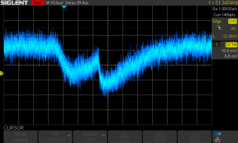
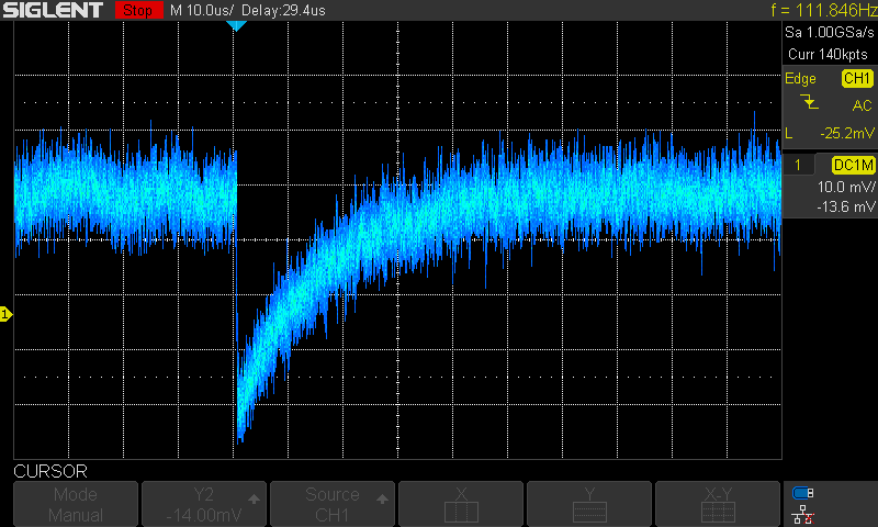
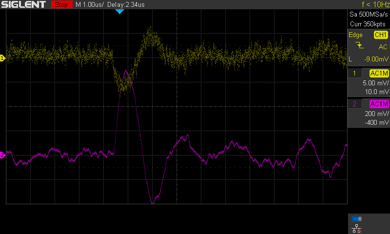
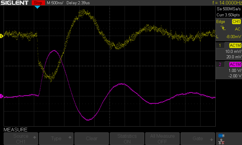
    Modified board was mounted in the aluminum box with an Am241 source. This time the diodes were not shielded with copper foil as the box provided enough shielding. Unfortunately, the box was not light-tight so I had to cover the diodes with a single layer of black isolation tape. With that the working point of the TIA was at 2,5V as expected - meaning that there were no additional currents shifting the operating point. Some of the captured screens show the output of the preamplifier:

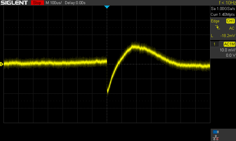
    Low energy pulse
    Two pulse pile-up
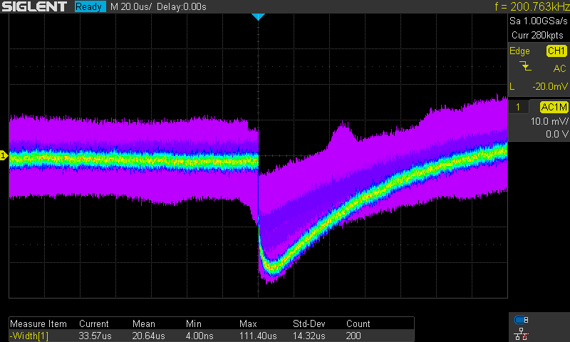
    High energy pulse

    Signal processing
    Having finished a fully functional preamplifier the next step was to process the raw noisy signal with the signal conditioner board. This was definitely more challenging as each segment had to be optimized in regard to the other blocks. Some of the values picked while evaluating the simulation did not provide required stability or operating points and had to be altered.

    General issues:

    • Resistors or inductors used in power supply filtering need to have low resistance around 1-10 Ohms as any greater value causes unacceptable voltage drop across them.
    • Double LED indicators on each side of the board are redundant as they signal the same thing. Only one group should be soldered.

    Filter

    6th order Bessel filter based on Sallen-Key topology may be instable when high gains are set due to required component precision values. In my case I had to reduce the gain of the whole block to 60 and recalculate all values again with ADI Precision Studio. A simple change in the divider at the output of the amplifier will change the gain but the stability of the filter will be decreased dramatically. I also noticed that the filter block was not designed with noise optimization option available in the tool. For any further versions I am considering the 4-stage Multiple Feedback topology with improved stability and proper noise optimization.

    Filter segment output with...

    Read more »

  • Third version prototype V3

    Marcin Wachowiak02/16/2020 at 15:09 2 comments

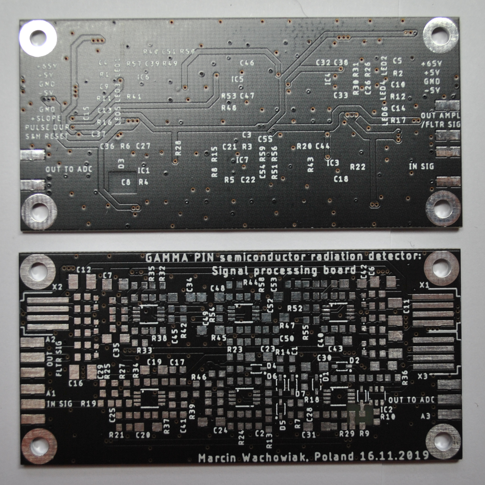
    Recently I have finished and produced the third version of the detector. Several improvements have been made considering the issues with the previous versions. All files including gerbers, schematics, boards and latest simulation can be found on my GitHub repository. Change log:

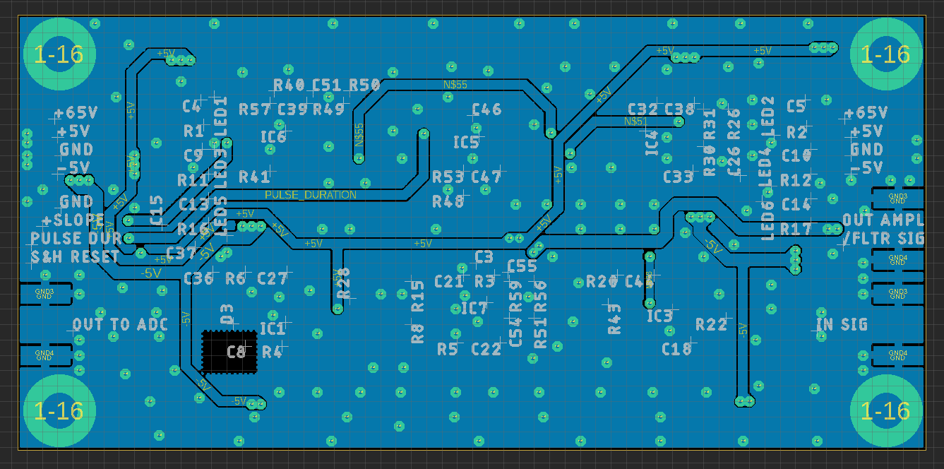
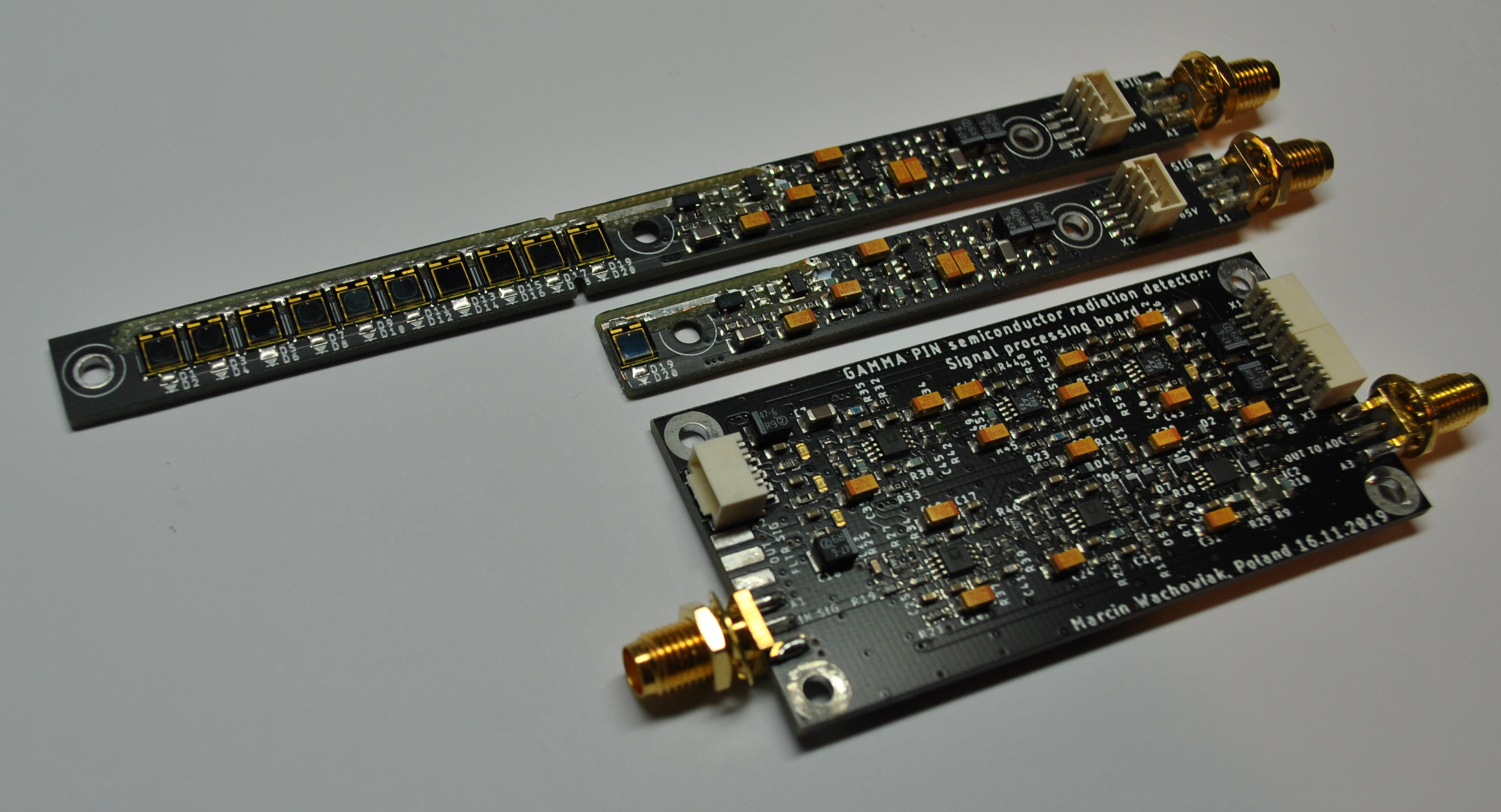
    • The whole circuitry has been split into two separate boards named accordingly to their function: preamplifier and signal processing. This helped to organize the components properly and extract less sensitive components outside of the detector chamber which is a crude metal box. Separating fast switching comparators from the charge sensitive parts is also an additional advantage. All signals are handled through SMA interface to ensure minimal external interferences.
    • Preamplifier segment required additional amplifier to boost the signal levels, before sending them to the processing boards. LTC6228 was added to handle this. Due to the fact that the design uses double amplifiers in a single package I had one additional amplifier left on the signal processing board which was used to increase the order of the low pass filter.
    • The bootstrapping transistor BF862 was replaced with CPH3910 as the BF recommended by a design note (https://www.analog.com/media/en/reference-design-documentation/design-notes/dn399f.pdf) has been declared end of life. You can still come across the BF in shops as retailers have some reserves. Performed simulations show that there is no substantial difference in the performance. Probably the noise figures are a little bit greater. You can view the results in the discussion below this log.
    • Signal processing board is equipped with “Filtered Signal” SMA output that can be used to connect the detector to a high-speed ADC or Multi Channel Analyzer for farther evaluation. This output is preceded by three stage low pass amplifier that can be altered to serve as normal amplifier without bandwidth limitation or any shaping effects.
    • Signal processing board and preamplifier are now populated with many bypass capacitors as recommended in the application notes. There is also an additional power connector on the signal processing board which is intended to forward the power to the preamplifier to avoid mess of split cables.
    • Preamplifier is now compatible with both VBPW34S and TEMD5010X01. There is additional milled line that should enable easy snapping or cutting of the board if you intend to use it with a single diode.
    • Around the charge sensitive path, a guard ring was introduced to minimize current leaks. Exposed and tinned trace is connected to the voltage similar to the input of the TIA. Although it is not powered by buffer following the voltages on the trace it may improve the performance a little bit.
    • At the bottom of the preamplifier an exposed pad was placed to provide grounding for metal screening of the diodes. You may simply solder the screen to mass without scraping the solder mask.
    • Molex pico-spox horizontal connectors (87438-04) have been replaced with vertical ones (87437-0443), as the horizontal ones are no longer recommended for projects. The vertical orientation helps to insert the plug and the cable can be easily bend to minimize the space taken up by the detector.
    •    
    Preamplifier board
    Preamplifier top
    Preamplifier bottom
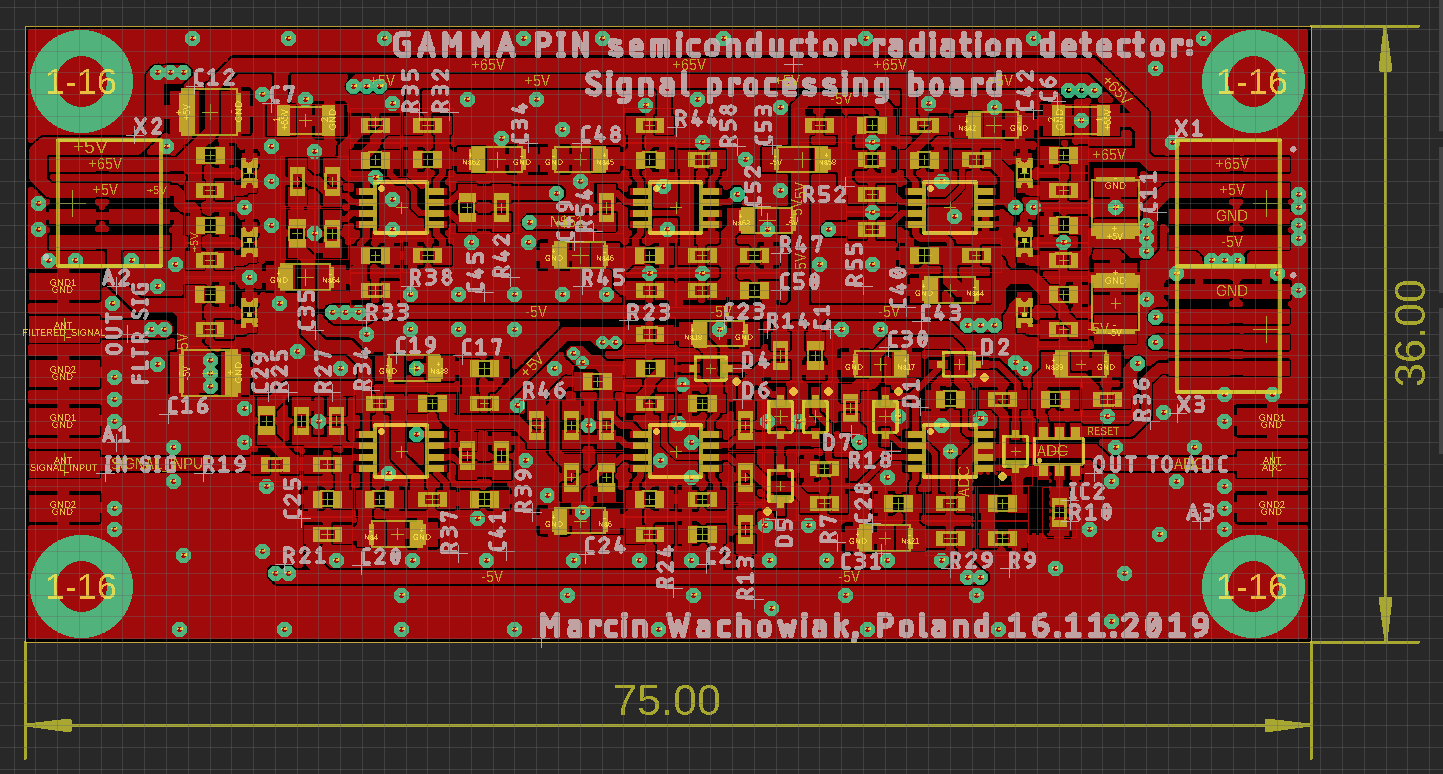
    Signal processing board
    Signal processing top
    Signal processing bottom

  • Optional improvements to the detector

    Marcin Wachowiak08/13/2019 at 19:25 0 comments

    Reducing noise contribution 

    The simulations I conducted in LTSpice show that even identical current pulses yield various voltage readings. The source of this distortion is a low frequency noise originating mostly from the detecting apparatus. Most of the high frequency noise is removed by the low pass filter, but the remaining passband range is enough to introduce a significant error. Using more selective passband filter is no help as its step response shape is invalid for peak voltage acquisition.   

    High resolution of the detector strongly depends on the repeatability of the detecting circuitry. It provides that certain energy of captured radiation is represented by a specified voltage level. When the response varies within the span of the error introduced by noise, peaks that should represent particular isotope become blurred. Thin lines become wide enough to cover other smaller peaks and hide significant details.

    There are a few ways of reducing the noise contribution:

    • Lengthen the primary signal timespan by increasing feedback resistance in the TIA. With that a more selective lowpass filter can be applied and reduce the noise according to the needs. Note that this solution increases the dead time of the detector and maximum count limit, so that more active sources may saturate the detector.
    • Use sensing elements with lower noise contribution and greater signal to noise ratio. In example: a photomultiplier tube with scintillator or high purity germanium or silicon detectors. In professional applications these devices are usually cooled with liquid nitrogen to really low temperatures to reduce the thermal noise to the minimum.

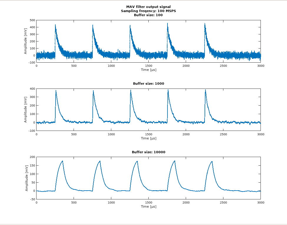
    Proposed solutions either require a compromise between the parameters of the detector or are costly and out of reach. However, there is a digital filter that can tackle this kind of noise better than any of the analog kind. The best solution to the noise present at the output of the sensing element is the moving average filter (MAV). Widely described in this article: https://www.analog.com/media/en/technical-documentation/dsp-book/dsp_book_Ch15.pdf.

    In short, the output signal sample is an average of all previous samples collected in a buffer of specified length. The samples are replaced subsequently by the newer ones, as the averaging window moves along.

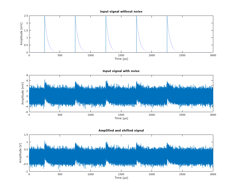
    Input signal visualization

    As a result, the noise at the input of the filter is averaged to almost constant value. Depending on the length of the averaging, buffer pulses present at the input of the filter are smoothened and signal distortion is significantly reduced. Moving average filter provides greater repeatability of results at the cost of using a high-speed ADC and FPGA as a signal processing unit. On the other hand, such change enables easy alteration of signal processing path as everything can be implemented and updated in the software. I performed a few simulations with MAV to see how effective it would be. Simulations were performed using Octave, but will run with Matlab too. (available in my github repository) The signal present at the input is similar to the TIA output in the real case. With 100MSPS and a buffer of 10000 samples I was able to reduce the error to 5mV. Thinking of the third prototype there will be an additional analog output pad in case someone would like to try this approach. 

    Filtered signal visualization

    In comparison the analog filter and baseline restorer do not remove the noise too well. In the worst case the amplitude may vary even by 60mV. I hope that the spectral distribution of the noise will be a little bit different and easier to handle than a uniform one present in the simulations.

    What is also interesting is that during LTspice simulations it turned out that the noise sources always have the same seed loaded. This means that the waveform of the noise signal will always be the same in each run. To see how the noise affects each peak I was forced to delay...

    Read more »

  • Designing and simulating the final version

    Marcin Wachowiak05/03/2019 at 19:42 0 comments

    After a long time spend testing and thinking about the right solution to all the problems, I have made multiple alterations to the current prototype. Some of them require a different design, so the new board including these signal processing units should be produced soon.

    Noise figures

    Almost all of the simulations I performed in LTspice were noiseless. The output signals were neat and easy to process. To consider a more real case I added a white noise signal to the output of the preamplifier so that it resembles 60keV pulses. After picking the right values I ended up with pretty dense noise of 8 mVpp and exponentially falling pulses of amplitude 2.5mV below noise floor. Such subtle changes rendered the old simulation completely useless. The old smooth signal was replaced with spiky and indistinguishable fluctuations. In the old version of the circuitry you could easily see that the peak value was repeatable, now it will be a lot harder.

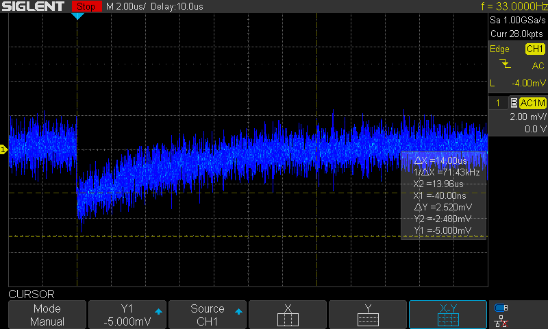
    Exemplary real case pulse (notice bandwidth limitation to 20MHz, reconstructed pulse has proper noise value)
    Reconstructed pulse in LTspice

    Updated approach to signal processing

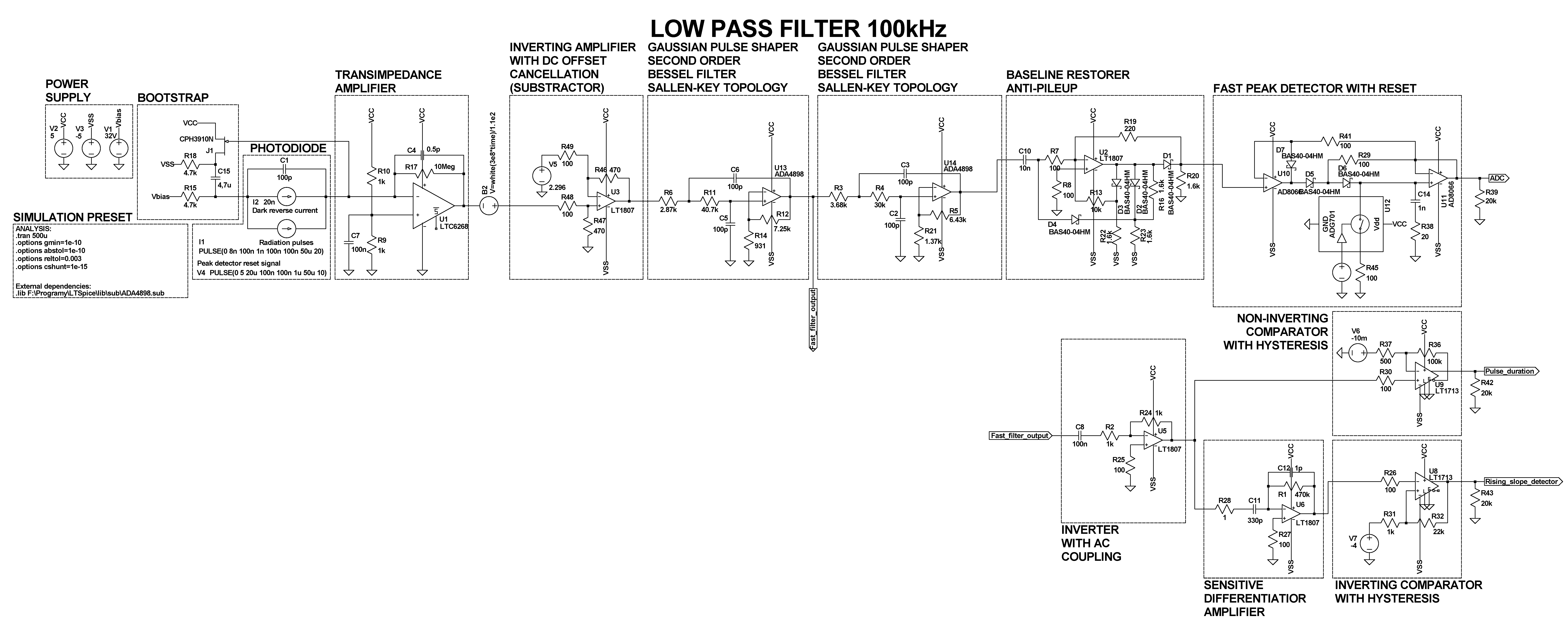
    Because of all that noise present in the signal I had to redesign the whole signal path. It will no longer have any subtractors or rectifiers which would have to be set individually. Instead there will be some new blocks, which will help to extract and measure the peak from the ever-present noise. Here is a detailed schematic:

    Schematic
    • Starting from the left the preamplifier feeds the signal to an inverting amplifier which is a preset subtractor. It reduces the DC of the signal close to 0V by subtracting the operating point of the amplifier which is about 2.45-2.50V. By this treatment the signal is ready for further processing without any undershoot that would be caused by capacitive coupling if we chose to use a capacitor to cancel the DC.
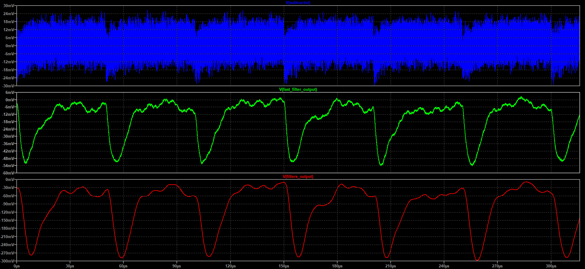
    • Next functional block is 4th stage Bessel low-pass filter implemented using Sallen-Key topology. The gain of the whole filter block is set to 50V/V and the corner frequency to about 100kHz. Its aim is to reduce the high frequency noise and shape the pulses so that they resemble gaussian ones. The delay and overshoot are crucial for this application as well as variable gain that can be suited to application. Because of these reasons Bessel type and Sallen-Key topology is used. To design these filters, I used online calculators available from Analog Devices and Texas Instruments. Notice that after the first stage the signal is fed to the comparator segment for further processing. It is necessary for the comparators to work with quickly shaped signal without huge distortions in order to give reliable results concerning pulse duration and its rising slope before it is properly shaped and prolonged.
      Pulse shaping by filters
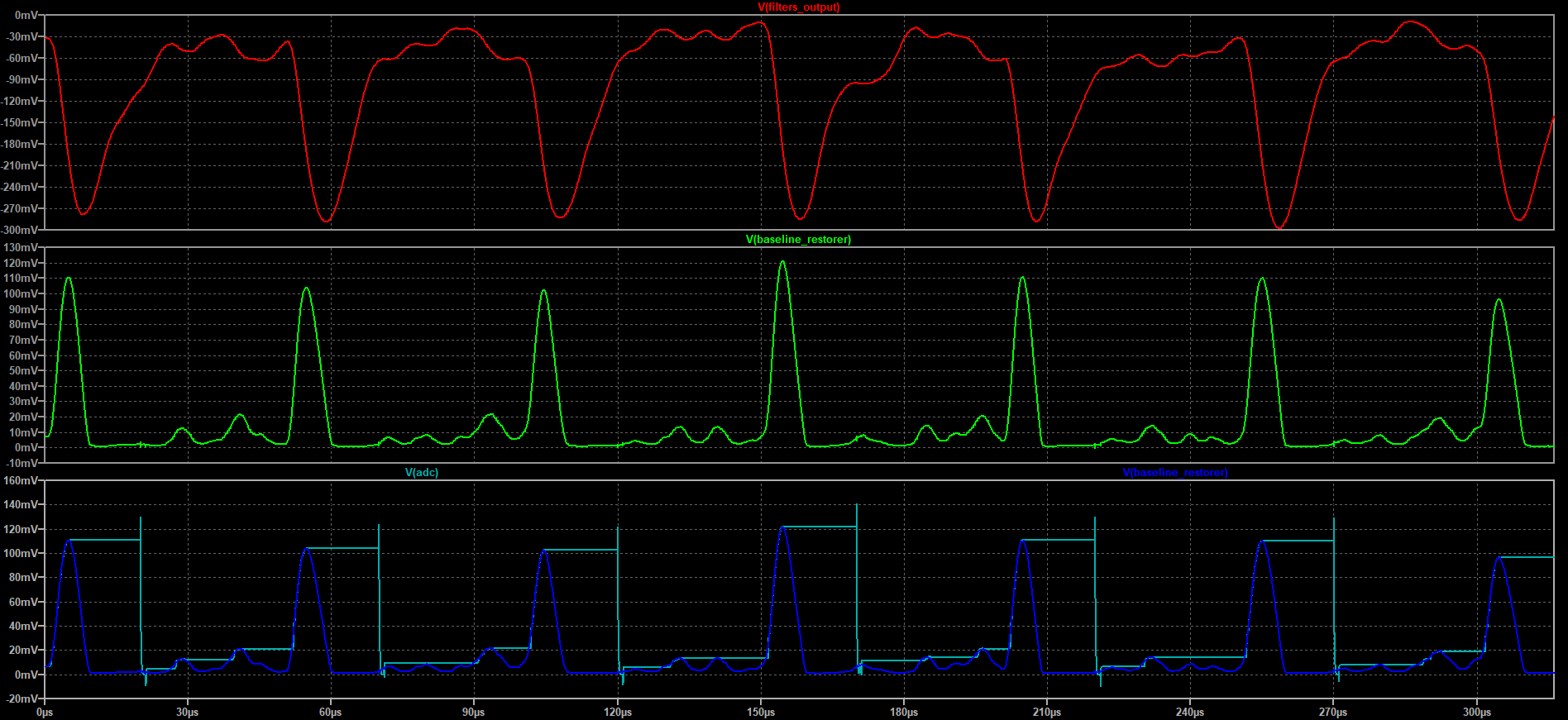
    • From the filters the signal is fed onto the baseline restorer which function is quite peculiar. Baseline restorer recreates input pulses removing any undershoot from the signal and providing pulse output height in response to the input signal level difference. With a proper baseline restorer any subtractors become obsolete and high dose rates can be handled without any errors caused by a temporary baseline shift.
    • The finishing stage of the signal path is a fast peak detector with reset. This time it is based on common amplifiers. Despite the fact it is fast and accurate. Its topology is extended to prevent capacitor discharge through rectifying diodes. Another addition is a digital switch serving as a reset, which will be triggered by MCU.
      Baseline restorer and peak detector signals

     Below the analog signal processing path is the semi-digital segment responsible for pulse detection:

    • The signal from the fast filter is AC coupled and inverted so that comparators can work with positive pulse without any DC. The undershoot does not play any significant role in this segment, because the amplitude is not that important as long as it is above a certain level....
    Read more »

  • Measurements, conclusions and upgrades preceding the third version

    Marcin Wachowiak05/02/2019 at 19:40 0 comments

    Evaluation of the preamplifier stage

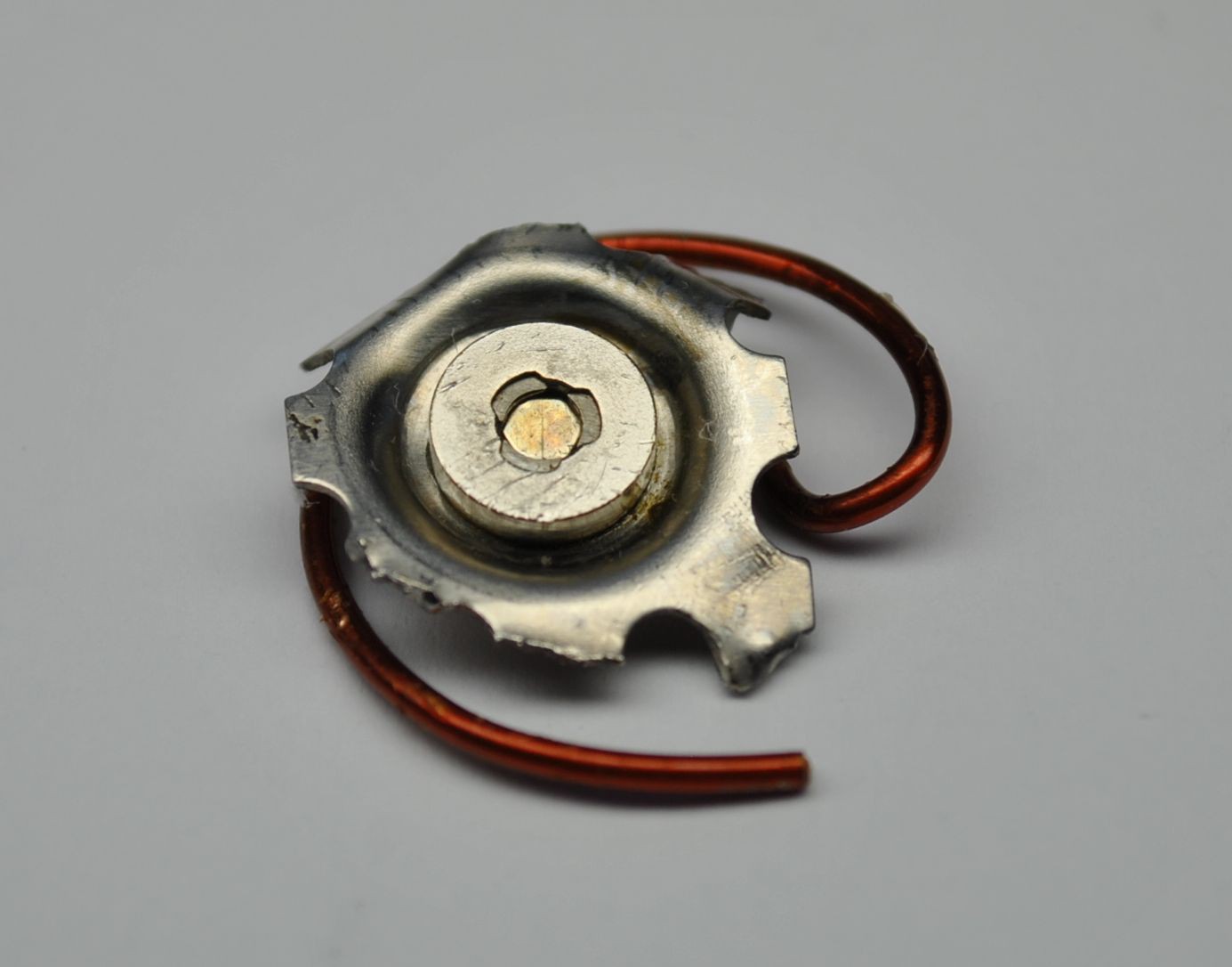
    To achieve the best resolution possible the charge sensing stage and its response had to be tested against various feedback resistance values. To conduct these tests, I used a source with known energy emissions. The only one I could easily acquire was Americium-241 from dismantled smoke detector. According to the Table of Radioactive Isotopes the detector should get readings of photons of energy of about 60keV (59.5412keV) which makes up for 35.94% of Am241 emissions.

    Am241 from disassembled smoke detector mounted on a metal plate

    Having a stable source, I was enabled to perform a reliable comparison while altering the circuitry.

    Bootstrap circuit alteration and efficiency

    As mentioned in previous logs I am trying to implement a bootstrapping circuit to be able to work with bigger – high capacitance detectors. Unfortunately, BF862 - the JFET used in the application note concerning bootstrapping is no longer manufactured. Moreover, the whole family of BF86X has been declared end of life. Although you might still come across it in some local shops, I had to find an equivalent to keep the project up-to-date. After a bit of searching the best, I could come up with was CPH3910 from ON Semiconductor. It has quite similar parameters and should be a fit substitute.

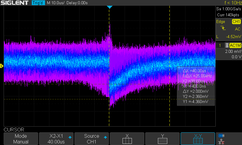
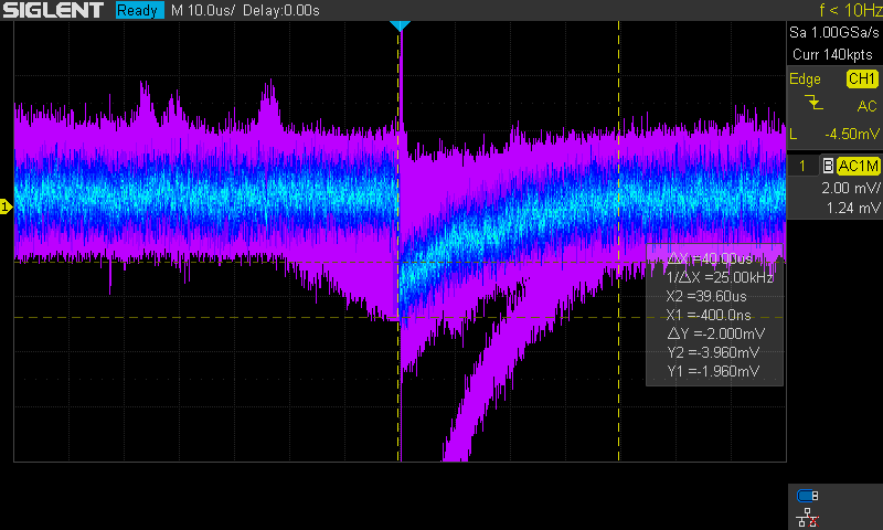
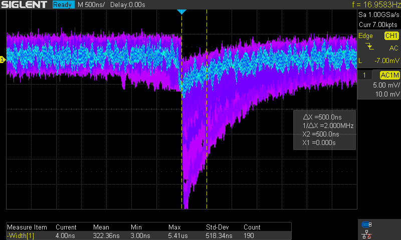
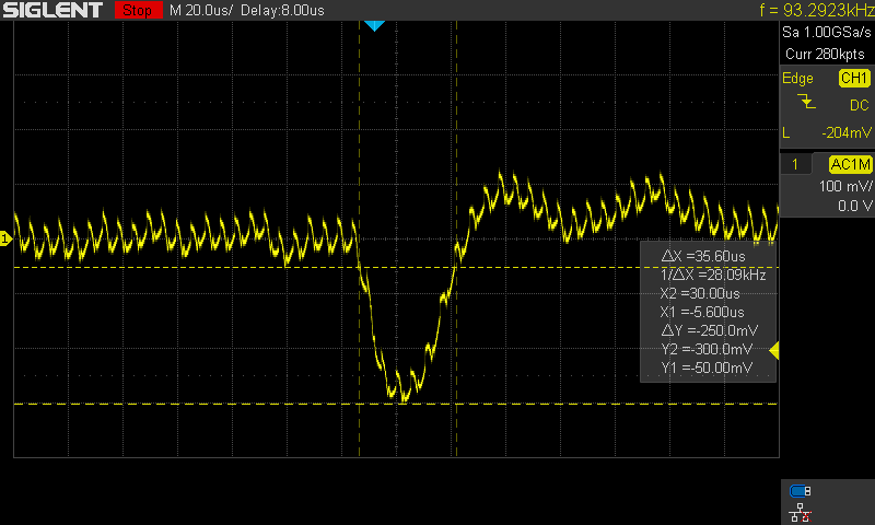
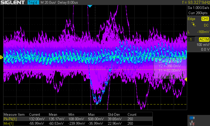
    To verify whether the bootstrap improves of degrades sensitivity I performed a few tests. The tests were performed in two configurations using 1 and 10 sensing diodes, respectively with and without bootstrap. With following presets: Source: Am241 (60keV), Rf = 22M, Cf = 0.47p, Oscilloscope BW = 20MHz and operational amplifier LTC6268. Notice that the values marked with the cursors are the ones that repeated the most – the most probable.

    The first test: 1 PIN diode:
    Without bootstrap - Bootstrap inactive 

    Collected pulses, one diode, without bootstrap

    With bootstrap - Bootstrap active 

    Collected pulses, one diode, with bootstrap

    In the one diode case the bootstrap had little impact on the signal quality because of the small diode capacitance. But from the noise figures I could read that it improved the low frequency components of the signal, which are more significant as the radiation pulses are in this domain. The pulse height did not change significantly enough in any way for me to notice. On the screen from oscilloscope you might see a trace of a high energy pulse, but that was probably just some random emission from the source which
    I don’t want to misinterpret. Maybe the bootstrap might have enabled the preamplifier to capture it.

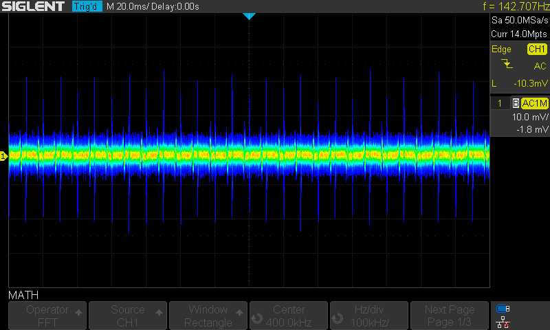
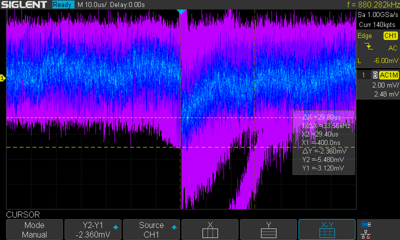
    The second test: 10 PIN diodes:
    Without bootstrap - Bootstrap inactive -preamplifier unstable:

    Collected excitation pulses, circuit unstable, 10 diodes, without bootstrap

    With bootstrap - Bootstrap active

    Collected excitation pulses, circuit unstable, 10 diodes, without bootstrap

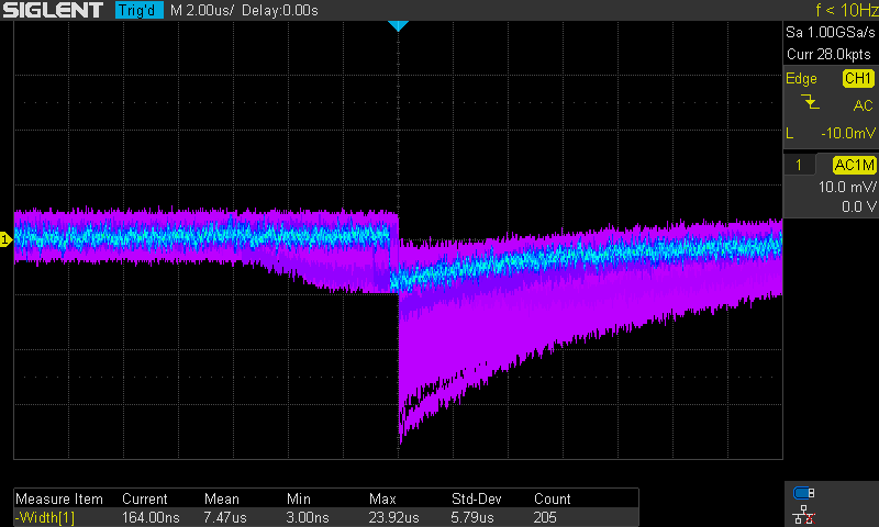
    Whereas in the 10-diode scenario the circuit was unstable without the bootstrap. It started to generate regular spikes as a form of excitation. After applying the bootstrap, the preamplifier became stable again. I checked the stability twice and in each individually assembled prototype the situation was the same. Even increasing the input capacitance did little to reduce the spikes of excitation, not to mention that it drastically decreased sensitivity. After returning to the preset feedback capacitance of 0.47pF and mounting the bootstrapping JFET the circuit once again detected radiation pulses. The bootstrap has helped to handle the capacitance of the diodes so that the amplifier excitation criteria was not met. Examining the captured pulses, it is clearly visible that 10 diodes introduce greater noise. Distortions amplitude has increased and there are greater fluctuations in the noise baseline. Despite the increased noise the undisturbed pulse height (below noise floor) remained approximately the same as with one diode. I also noticed a tendency that greater energy pulses...

    Read more »

  • Improvements to the second design

    Marcin Wachowiak10/06/2018 at 12:24 0 comments

    The first prototype is quite fine but it has some errors that I noticed during the assembly and testing. The detector will be still developed. I hope that the second version will be satisfactory enough to meet the requirements for the first spectroscopy. During the tests I became acquainted with the STM32 ADC and DAC. The detector is so sensitive that uploading the program to the development board caused oscillations. Having noticed this to prevent additional digital noise I decided to use non-volatile programmable potentiometer. Once the value on the MCP4161 is set. It will be disconnected to except any distortions from the signal busses. I am currently working with NUCLEO-H743ZI but after the prototyping is finished the detector should run with a “Blue Pill” board featuring STM32F103C8 microprocessor that should handle everything easily. 

    Things to improve:

    The signal processing

    • In the first version the pulse from TIA is simply amplified three times and then "lowered" so that only the meaningful peaks are positive. Then they are acquired by the ADC. Apart from the desired signal, the noise is also amplified. It results in distorted and spiky pulse with very short peaking time, blurred amplitude and unnecessary restriction of op-amp amplitude range. The capacitive coupling of the inverting amplifiers also causes massive undershoot and tail oscillations, that disturb the baseline and amplitude of the following pulse.
      Signal after amplification with visible distorted peak
      Signal after amplification with visible tail oscillation - baseline fluctuation
      • To avoid the pulse distortion the noise floor should be removed first and then the resulting peak should be shaped to resemble the gaussian function. It can be done by using 3-4 op amps just by changing the order of the processing. First there should be a subtractor that will "lower" the signal in order to make only the significant pulses negative. Then the signal is fed to an ideal negative rectifier based on another op amp. Finally, it's processed by double Sallen-Key filter which serves as Gaussian shaper. After these alterations the signal is connected to the acquiring segment by a single decoupling capacitor so that its normal level is around 0V.
      • The simulations with the described above configuration nicely visualize the signal processing. To improve accuracy in the LTspice model I added a white noise current source in parallel. It should resemble the thermal noise of the semiconducting PIN diode.


    Old version simulations with noise

    V1 prototype with noise source added
    Current pulses with noise background
    Singal after processing with V1 simulation model
    Signal after substraction

    New version configuration

    V2 simulation schematic
    Signal after the first stage of substractor and rectifier
    Previev of the signal shape through the circuitry
    Output signal suitable for farther processing

    Supply filtering

    •  Fast, wide bandwidth op amps and comparators generate interference that unfortunately excites more sensitive parts. The whole detector is extremely sensitive to any change of charge. The additional pulses generated by switching caused it to oscillate. At first, I thought this was caused by the high integration of the board and crosstalk. But in the end, it turned out to be just lack of decoupling capacitors, that easily prevent the excitation. The few capacitors placed at the distant end of the board were not enough.
      • To solve these instability issues, every integrated circuit supply node will be powered through a 100 ohm resistor with two capacitors attached. One ceramic 100nF and one tantalum 4,7-22uF placed as close to the pins as possible. It may seem overengineered but it is neither an expense nor it would have saved lots of space on the board.
        Set of capacitors, each connected to its own IC

     Compatibility

    • My aim is to make this detector an accessible tool to measure and analyses radiation. Therefore, I have...
    Read more »

  • Tests and measurements of the V2 prototype

    Marcin Wachowiak09/07/2018 at 15:28 0 comments

    As the boards arrived I started the assembly of the first prototype. The power filtering first and then the sensing and the transimpedance sections. There was a serious mistake in the BPW34 Eagle library - dot marking the anode was at the wrong side of the part. Unfortunately a few of the diodes were damaged after I found the cause.

    Proper TIA feedback resistance value

    Currently I am focused at the TIA stage and the proper signal processing. With a live working detector, I am able to measure the real data and see the simulated circuit in the real conditions. There is a significant dissonance between the simulations and real circuits in this case.

    Here are some results I gathered with a few Rf values:

    I also conducted tests with the value of 1 Giga Ohm, but no pulses were detectable even with the radioactive source present. The op amp that was used (LTC6268) had a bandwidth of 500MHz, there is also an upgraded version of it with the BPW of 4GHz, I hope to test it soon and see if the optimal working point will shift upwards in favor of greater resistance values. From the data gathered I estimated that the Rf value should be somewhere between 1-10M Ohms. I guess aiming at the 2,2 to 4,7M will provide the pulses of length about 1us with the sufficient amplification and sensitivity - ideal for subsequent processing.

    Noise issues

    The new detector design is extremely sensitive to noise. The PIN diodes generate a lot of it and additional high voltage sources like energy saving lightbulbs or CRT affect it and distort everything. The simple switching of a soldering station renders a spiking in the signal. The shielding is an absolute necessity unless the circuit is enclosed in a grounded metal case where the measurements will take place. The noise level is about 12mV peak to peak, but still the pulses are distinguishable, which is nice.
    I am thinking of a new way to process the signal to prevent the undershoot and eliminate the constant noise level at the early stage by a simple subtractor and ideal rectifier circuits made with op amps. Then an additional stage of two Sallen-Key filters acting as a gaussian shapers and the signal would be ideal for acquisition.

    Rf = 100k measurements:

    Rf = 1M measurements:

    Rf = 10M measurements:

    Rf = 100M measurements:

  • Finished new prototype design

    Marcin Wachowiak08/21/2018 at 09:24 0 comments

    After two weeks of designing the PCB and optimizing all the routes I finally managed to send the Gerber files to manufacture. As previously mentioned I wanted the board to be in a shape of a thin stripe, so the result is board with all components on one side having dimensions of 160x11mm. Whole design is with regard to parasitic capacitances, that should be minimalized to allow the best performance.
    The detecting "stripes" may later be aligned to form a multi-layer matrix to perform some particle trajectory or coincidence research. I have aimed to make it quite universal so there is a dashed line where the board may be cut to solder the photodiode in right angle. There is also an option to bypass the MCP4161 by connection its 2nd and 6th pad which are in a straight line and use external DAC to set the noise cancelling level.

    Board design
    Gerber files view

    I ordered 50 boards from the JLCPCB, so if you want to test this design contact me and I may sell some to you. The schematic includes all the blocks mentioned in the description and some additional capacitors for filtering the power lines. The power stabilizers and IC are to be located on external board from which all the stripe detectors will be powered all together.

    Schematic of the next prototype

    In a few days’ time when I get the boards I shall begin assembling the detector stage by stage to test it all. I have acquired all the necessary parts and am ready to proceed to the next stage.

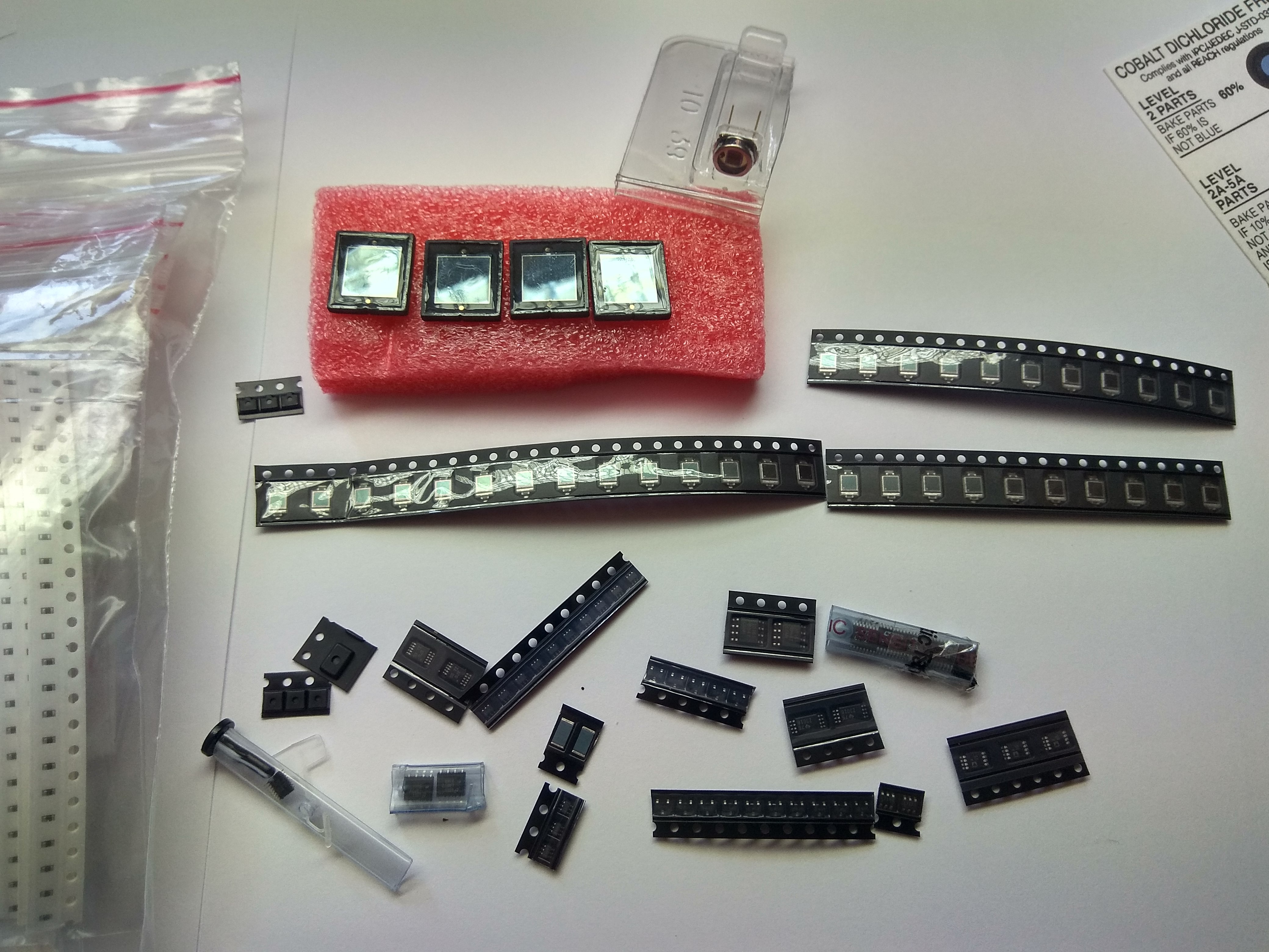
    Parts for the assembly

  • Inconclusive simulations

    Marcin Wachowiak08/01/2018 at 12:00 0 comments

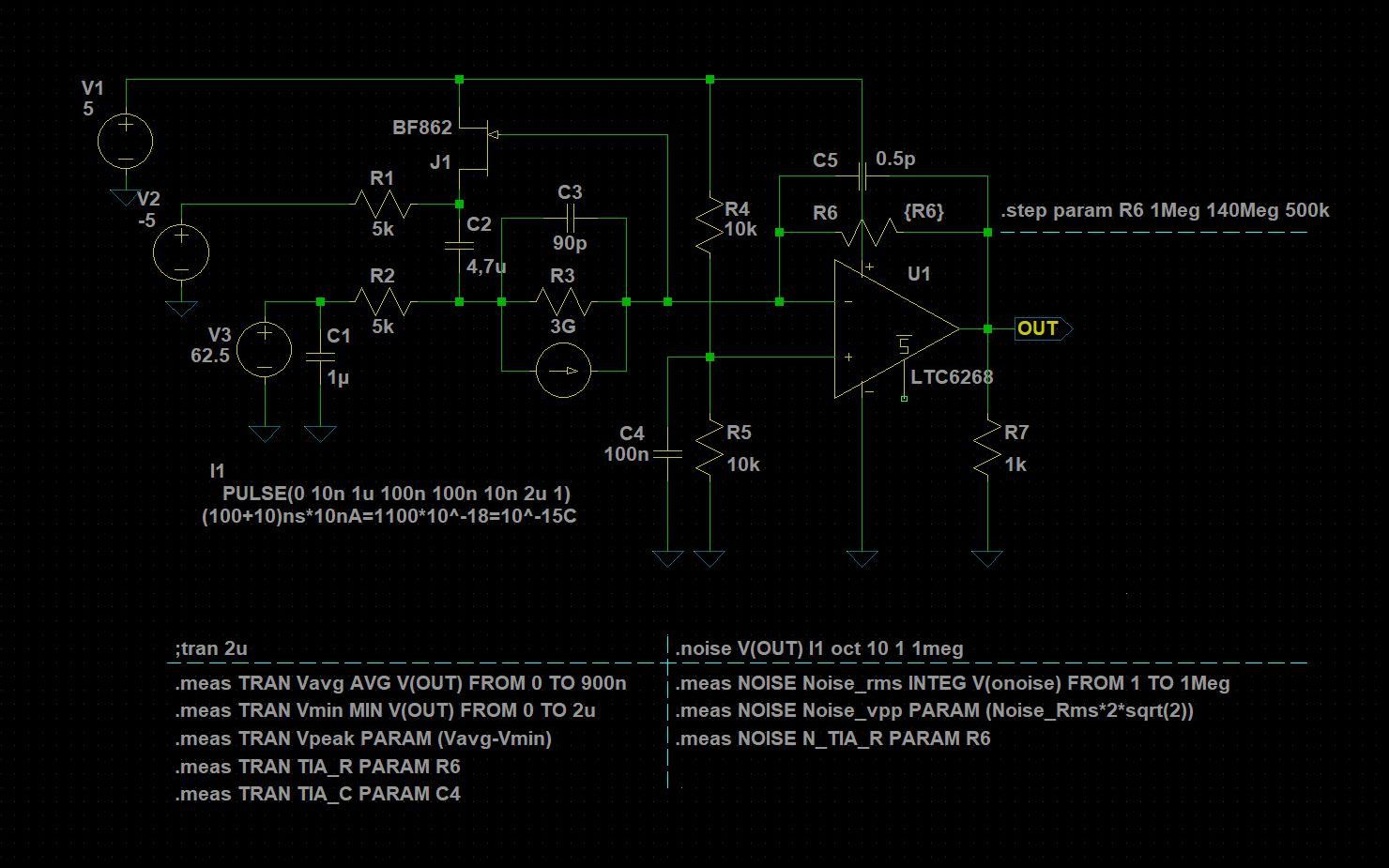
    Recently I have tried to simulate the transimpedance amplifier once more to optimize the components for the best singal to noise ratio. This proportion is mostly affected by the feedback resistance, which determines how large the output signal will be. The additional feedback capacitor shuld be kept at lowest value preventing the op amp from disastrous oscilations.

    Simulated circuit

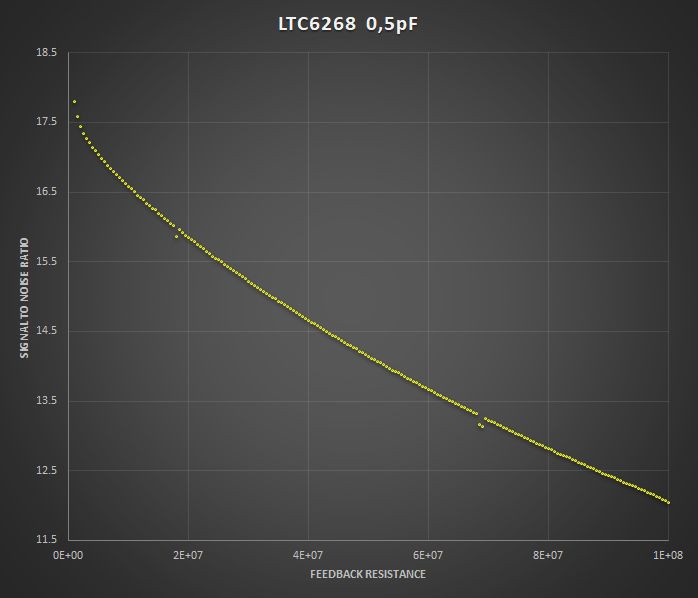
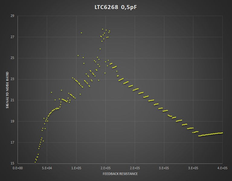
    The pulse coming from the detector had an estimated length of about 300ns and carried charge of one femto Coulomb. The feedback resistance was stepped in two scopes one ranging from 1M-100M. The other one was more focused on the peaking that ocurred in the scope 10k-350k. For resistances greater than 140M the simulations didn’t provide any reliable or sensible results. Results of this analysis also varied with the noise integration range. For this case I have set it to be from 1Hz-1MHz.

    Rf: 1M-100M scope
    Rf: 10k-350k scope


    Estimating results even in the simulations is really complicated as all the parameters are dependent on one another. This circuit needs to meet a few criteria:

    • Huge amplification for the ultra low current pulses
    • Highest possible SNR - Signal to noise ratio
    • Wide bandwidth to amplifiy even the shortest events and measure high doses

    This simulation does not include the thermal noise coming from the photodiode and the numerical analysis has its limitations. In the range of extremely large resistances or low currents it is unwise to relay only on them. Even though I ran lots of simulations still the results varied depeding on the scope. Finally, I decide to design the board and work on the prototype to pick the optimal values. One part after another I will assembly the detector and gather the data that earlier I could only estimate without certainty.

    The first examination will focus on the TIA - transimpedance amplifier . I intend to focus on the feedback resistor to see what results provide various resistors starting from 100k to 1G. I'm also curious about the noise from the photodiodes.

    If you have any suggestions about the simulations I am open to any discussion as it feels a little bit as if I was walking in the dark. I wish I could find one and only optimal value for the TIA, but the whole thing seems to be floating. Maybe PSpice has some better numerical analysis or tools, but unfortunalety the LTspice models/libs are coded and availible only for LTspice.

  • Evaulation of the old prototype based on TL072

    Marcin Wachowiak07/28/2018 at 15:16 0 comments

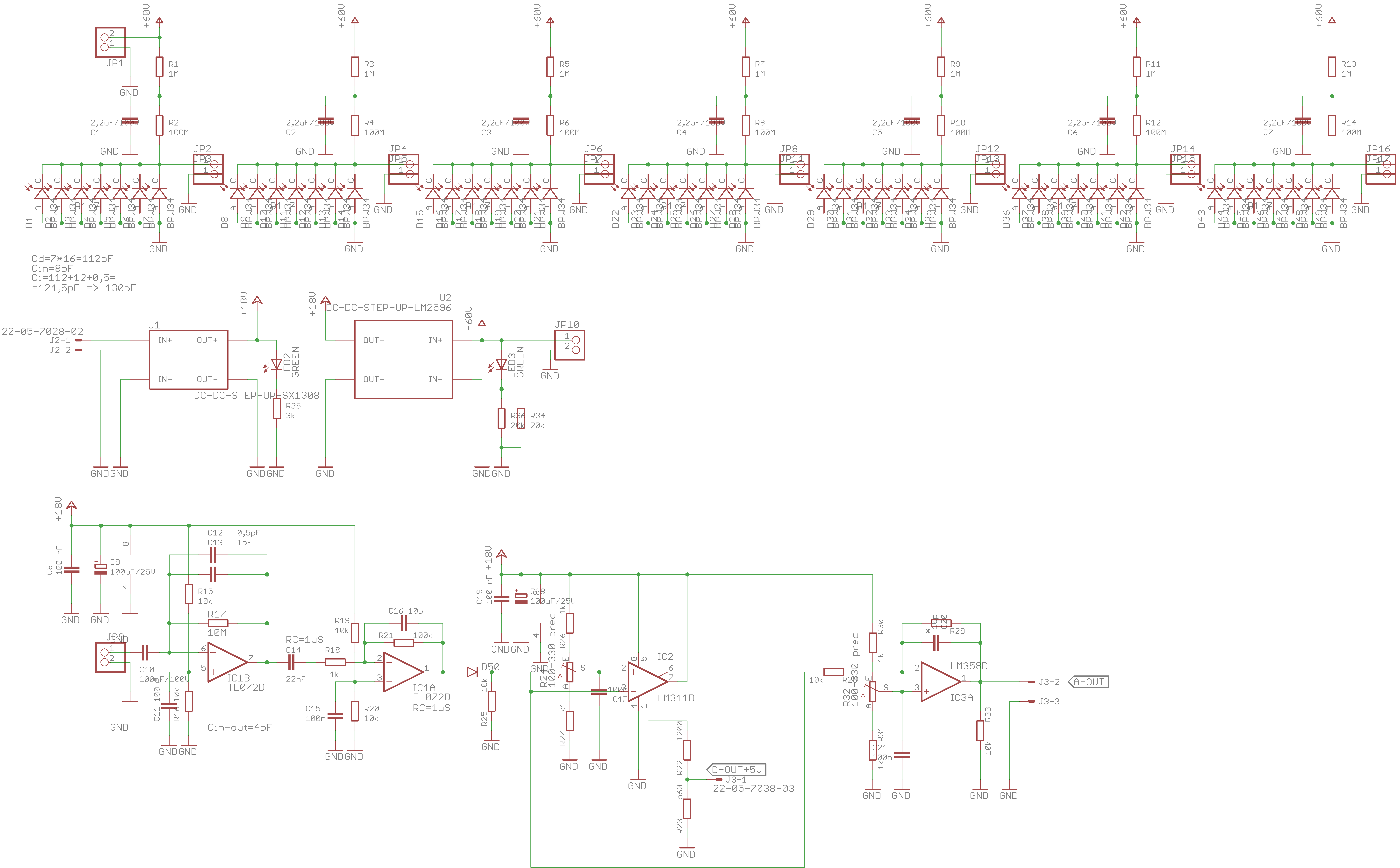
    The early stage prototype of the detector was designed to have an array of about 50 PIN diodes.
    To distribute them equally I divided the array into 7 rows with 7 diodes each. Every single row had
    it’s own sensing amplifier construced using TL072. This common and easily accesible solution was supposed to give me an insight to futher work with this kind of detectors. The design was preceded with simulations in LTspice to check what results may I expect.

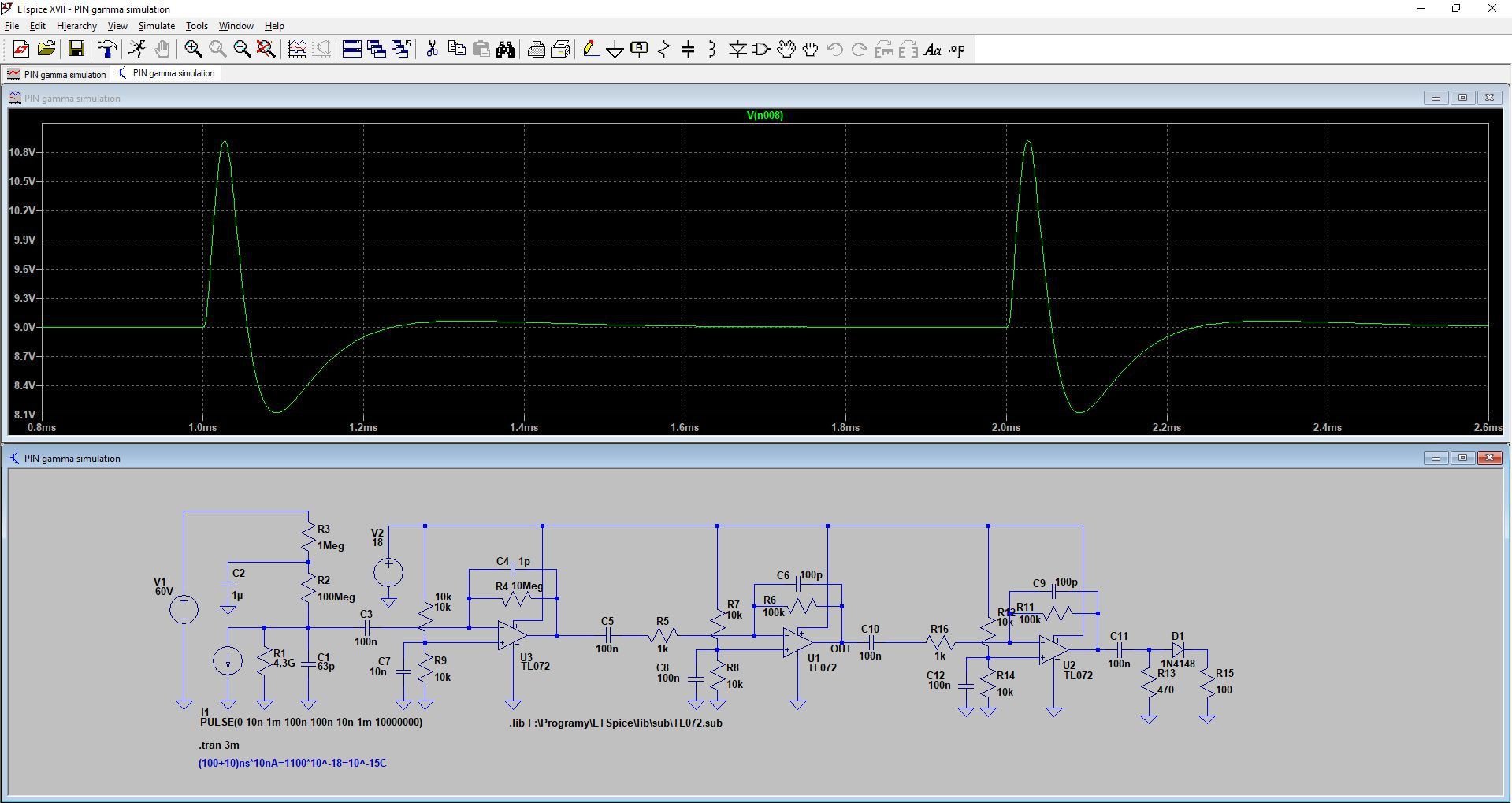
    LTspice Gamma PIN prototype simulations
    Early stage TL072 design


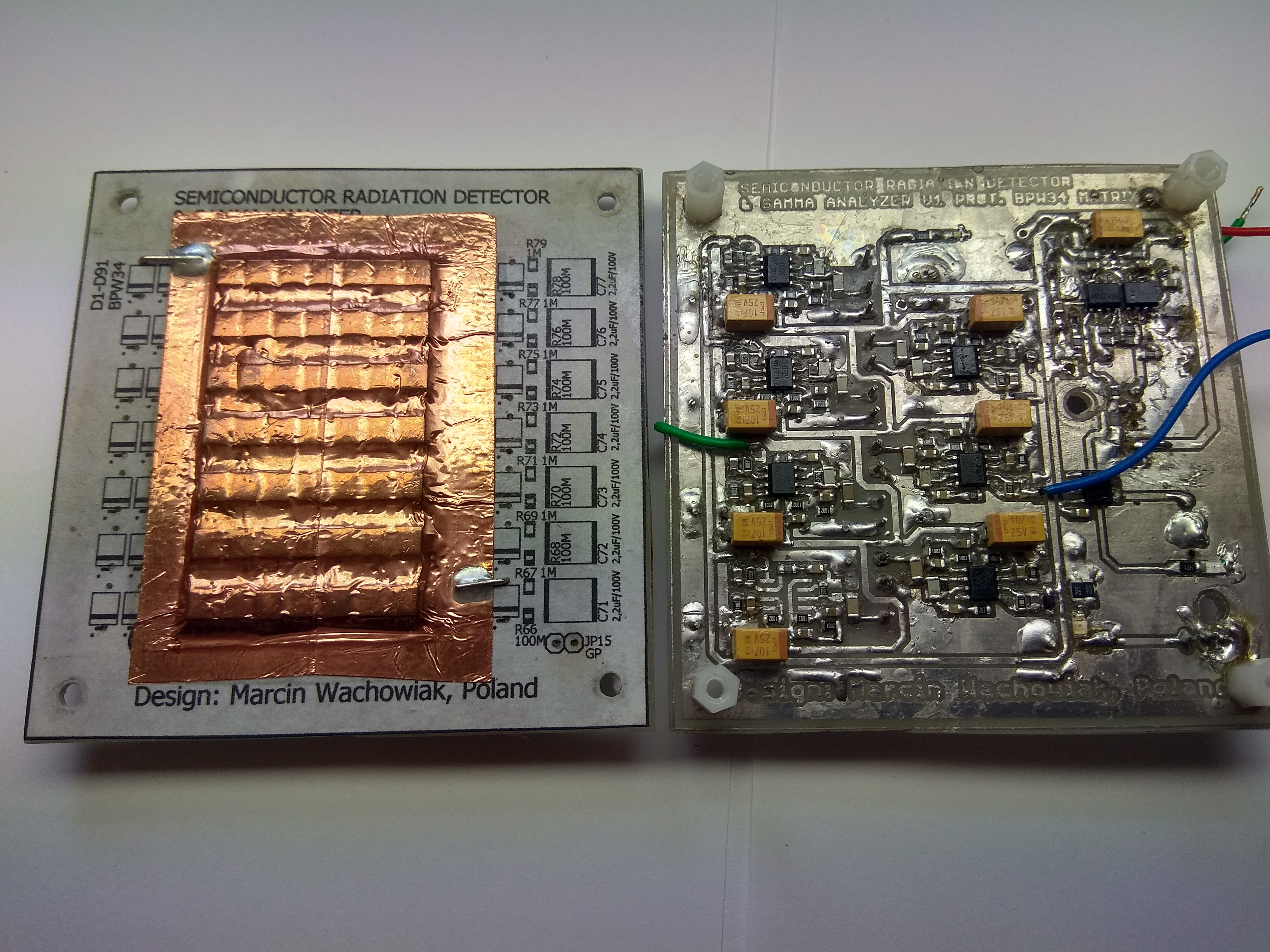
    This prototype was created in a wafer fashion to make it smaller and stackable. The power supply was based on common step-up inverters using LM2577. By changing the feedback resistor they may work up to 65V. TL072 worked at 18V and diodes were biased by 60V. These power modules were shielded to reduce the noise emitted by the coils.

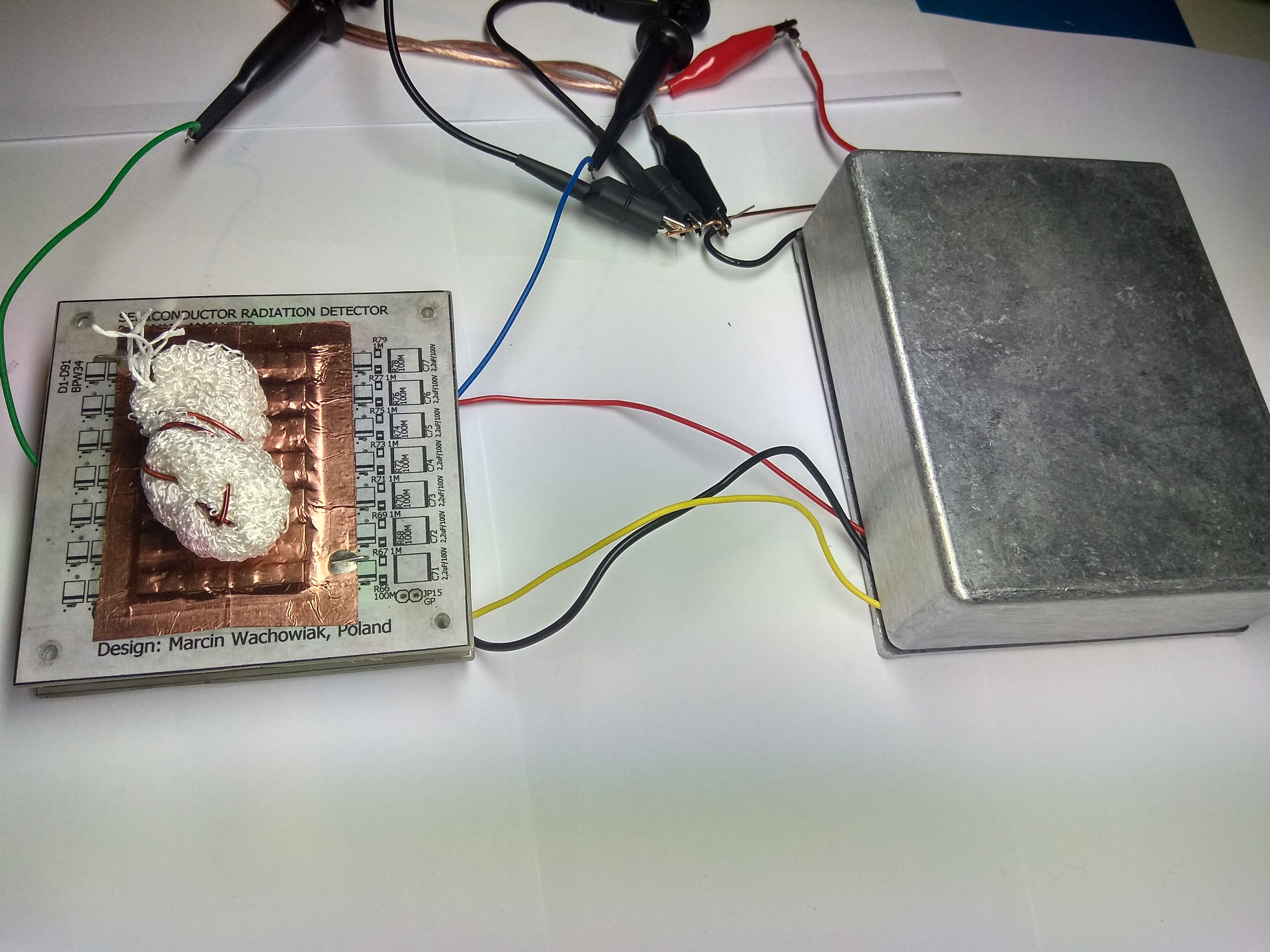
    Whole device
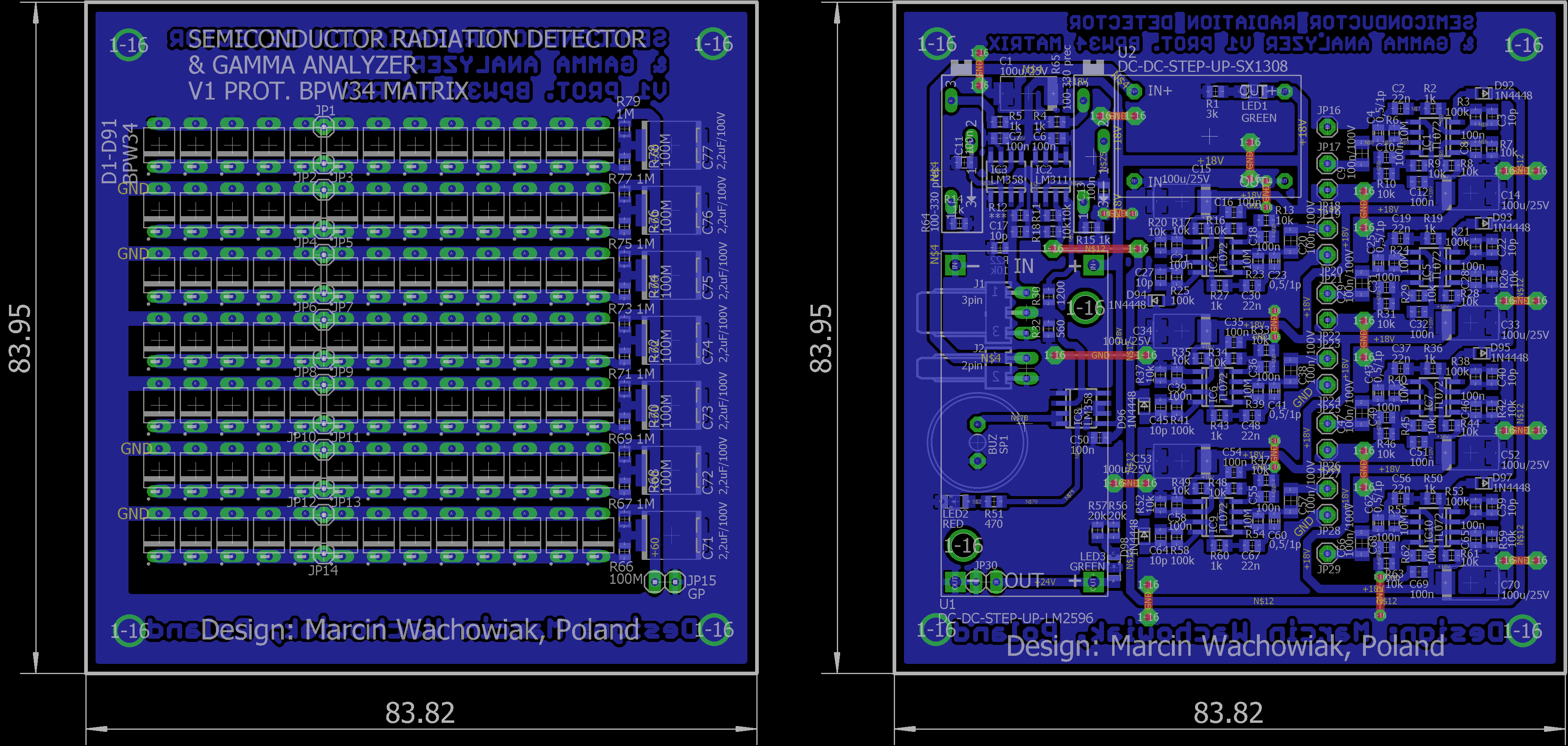
    Board footprint


    Unfortunatelly, in the final stage of the signal processing there have occurred an error stopping the grid detector from functioning properly. The pulse signal is negative and in the circuit there is diode added at the output of the TL072. It was supposed to prevent the signals from mixing if they were positive. This awful mistake is still present in the PCB files. If you wish to test your own detector make sure you have replaced the diodes with a proper solution that would stop the signals from interfering.

    Schematic of the early design


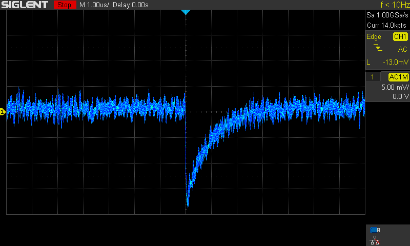
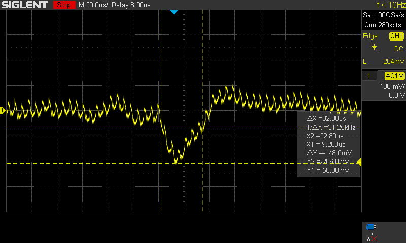
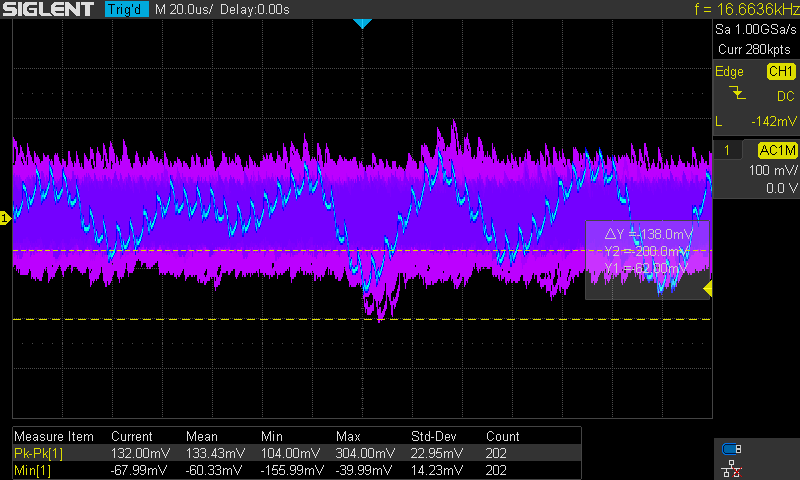
    I still managed to get use of the single row to measure some radiation. The first measurment was without any source. Even the background radiation managed to leave a trace, although the pulses were significantly smaller and happened less often.


    Low energy pulse coming from the background radiation

    Image of the collected pulses through short time with no source present

    Then I placed a thoron mantle at the sensing area. Simultaneously the pulses were higher and more frequent. For a single singal trigger I didn’t have to wait even a second.

    Detector with a thoron mantle placed upon it

    High energy event - particle coming from thoron mantle

    Pulses collected with the source present


    On the whole, this prototype has allowed me to focus on a few problems that will need to be solved:

    • Noise and parasitic capacitance should be kept as low as possible. The whole instrument for proper working conditions, will have to be enclosed in a grounded metal chasis.
    • The power supply circuits will need to be with reduced EMI and voltage ripple. This induces
      me to use charge pump voltage regulators, which should be suitable for the job.
    • For any future applications the single row detector should be made modular and portable to enable easy use. The sensor will be in a shape of a thin stripe with a connector at the edge.

    The early design was quite a crude one. The second one is going to be well thought over to provide reliable results.

View all 10 project logs

Enjoy this project?

Share

Discussions

Jo Verbeeck wrote 07/23/2019 at 19:45 point

Very nice project! I wonder if a fast adc and doing pulse shaping in the digital domain would not be more performant, but very likely the cost will be higher. Red-pitaya or some sdr hardware may do the trick with existing hw. I would love to see these. Having an output sma plug before the pulse shaper but after the initial amplifiers could help to test this setup later. I do have a commercial 8 ch digital pulse processor available that could do just that.

  Are you sure? yes | no

Marcin Wachowiak wrote 08/13/2019 at 19:44 point

Thank you for your support, digital domain seems to be very promising since various ideas can be implemented without physical modification. There are also new, better solutions like moving average filter.  I hope to try this approach by attaching a fast pmod ADC module to Digilent Cora evaluation board and properly programing the signal path. But first I need to either design this ADC module or find one adequate for the detector (about 100MSPS and 12-14bits). In the coming third prototype there will be an SMA connector for this kind of signal processing.

  Are you sure? yes | no

fabian wrote 07/27/2018 at 14:43 point

No dobra a do czego to?

Wiem, że obrazowanie taonowe było uzywane w piramidzie do określania gdzie są korytarze, nawet detektory materiałów rozszczepialnych sa na granicach i wykrywaja co ktoś przewozi. Chcesz zrobic coś co bedzie wykrywać przedmioty ?

Jak czułe jest to coś? Może jakas farba jest metaliczna? np. jak przeczytac tekst na kartce, której nie widzisz bo jest wewnątrz listu (druk gazetowy ma chyba ołów)

  Are you sure? yes | no

Marcin Wachowiak wrote 07/27/2018 at 15:04 point

Na razie do mierzenia natężenia promieniowania, potem jak już uzyskam dobrą czułość po zbudowaniu drugiego prototypu do spektroskopii jądrowej i analizy jakie pierwiastki promieniotwórcze zawierają różne substancje. Np. suszone grzyby - cez, banany - potas itp. Ale to wszystko jest jeszcze w fazie rozwojowej. Pierwszy prototyp dawał średnie rezultaty bo był zrobiony na łatwo dostępnych częściach, ten powinien być znacznie lepszy. Można to potem rozbudowywać o trajektorie cząstek czy tworzenie obrazów prześwietleń. O tym pierwszym zaraz napiszę w logach.
  Are you sure? yes | no

fabian wrote 07/28/2018 at 08:36 point

czyli cos jak w startreku do mierzenia wszystkiego. Kiedys byla kampania na kickstarterze do takiego urządzenia. Może i Tobie się uda. Czy możesz wycisnąć jeszcze kąt padania? Kiedyś widziałem detektor w formie stołu gdzie można bylo zobaczyć miony na całej powierzchni. Wyglądało niesamowicie. Ale mając też wygląd może jeszcze coś dało by się wyciągnać z badania. Może w zależności od układu promieniowania są jakieś właściwości.

banany akurat mają promieniotórczy potas 40 chyba. Ja bym się bardziej bał strontu 90 czy cezu 137 co swoja drogą wykryto ostatnio w winie w USA (mowi sie o przecieku z fukusima) no i nasze ulubione nawozy sztuczne.

czy promieniowanie oddziaływuje na siebie? np. czy promieniowanie jednego pierwiastka opóźnia dugi? dwa grzybki obok siebie.

Moim zdaniem obrazowanie jednak ma wieksza przyszłość niż spektroskopia

  Are you sure? yes | no

Marcin Wachowiak wrote 07/28/2018 at 12:37 point

Zobaczę ile uda się osiągnąć podczas budowy tego detektora. Żeby obrazować najpierw muszę mieć sam spektroskop i nim mierzyć nim energie po przelocie przez jakiś materiał. Analizując jak duże straty wystąpiły przy przejściu może uda zrobić mały obraz gęstości ośrodka. W przypadku pomiarów obecne będzie pełno efektów rozmywających dokładność takich jak: cząstki/kwanty odbite od osłony próbki, różne energie dochodzące z różnych odległości dla niesymetrycznego źródła. Nie powinny one znacząco wpływać na pomiary ale będą wprowadzać błąd statystyczny.

  Are you sure? yes | no

Similar Projects

Does this project spark your interest?

Become a member to follow this project and never miss any updates