-
Added the clock to the Tell Time Contest
01/19/2020 at 17:26 • 0 commentsThe clock that was built with the 1-square-Inch CPU was entered in the Tell Time Contest, you can see the entry HERE.
And a few months ago, this CPU was featured on Hackaday !
I also entered another clock to the contest, the Forklift clock .
-
CPU article by Cabe Atwell
09/05/2019 at 12:48 • 0 commentsI am very proud to see that Cabe Atwell wrote about this project and the Kobold computer on Hackster.io ! Read the article HERE !
-
Building a full computer around it
04/09/2019 at 18:11 • 0 commentsToday, the idea of the KOBOLD computer was published here at Hackaday. You can find it here: Kobold - retro TTL computer
-
Clock simulation on webpage working
10/25/2018 at 17:48 • 0 commentsThe 6 digits of the clock are added to the Javascript simulator/assembler and are fully functional now. They are addressable in the same way as in the real hardware. You can open the page, press "assemble" and then "run" to see the clock working, driven by the same software that runs on the device itself. (But pressing run without having the code assembled will hang the script, be warned).
The simulation runs at 1200 cycles per second (depending on your computer and browser speed). That is a bit too slow to have the clock running exactly in the same way as on real hardware. The clock software has a prescaler that counts four edges on the 2Hz hardware signal, to get a one-second tick. The simulator has been tweaked to disable the prescaler, and the one-second-signal is simply generated after each multiplexing "frame" (so the counter is free-running and not coupled to real seconds). The memory locations that are used by the prescaler (0x058 and 0x0030) are manipulated by the simulator. The clock software itself is unchanged. Buttons for setting the time are not available in the simulator, mainly because the software would not scan them frequently enough.
In the files section, the software zipfile was updated with this new version.
Note that you can just change the software in the leftmost window, press assemble and run, and see how the program behaves ! For instance, it is easy to change the starting time of the clock from 00:00:00 to another value.
-
Schematic of the CPU
10/21/2018 at 10:44 • 0 commentsTime to fully disclose the operation of the CPU ! The complete schematics can be found in the files section, SQ1C1841.PDF.
REGISTER B
![]()
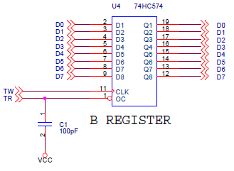
Let's start with the simplest part. Since the CPU has no ALU, the most important task of the CPU is moving data from one place to another. So in one cycle it fetches a byte from memory and stores it in the B register. In the next cycle, it can put the contents of the B register on the databus and store the value somewhere. So the B register can be loaded from the databus (at the end of a low pulse on TW), and its contents can be placed on the databus (when TR is low).
The signals are called TR (T-Read) and TW (T-Write) because the B register was previously named "Temp".
In the decoder part you will see that the write and read signals come almost at the same time. It was expected that at the end of these signals, the databus would keep its last signals for perhaps twenty nanoseconds after the '574 was tri-stated at the end of the TR signal. But this did not work, so the TR signal had to be delayed by a small 100pF capacitor. This capacitor was not on the first version of the board. It is also not on the NAC pcb, it must be added on the NAC as a modification.
Note that the low side of the capacitor is connected to VCC (5 volt) instead of ground, this is because it was impossible to make this connection to ground with a trace on the pcb. But it was possible to connect it to VCC, so that was chosen. It makes no difference for the operation of the capacitor.
ADDRESS GENERATION
![]()
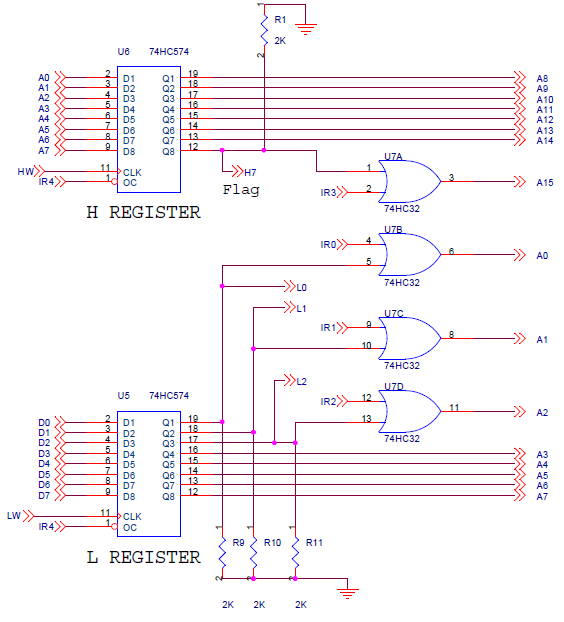
The L register can be written directly from the databus by making LW low. The output of the L register generates the address bits A0 - A7. Note that the lowest 3 bits are OR'ed (with HC32 gates) with the microcode bits IR0 - IR2. In most cases, only IR0 is used (when the H and L outputs are active), to select either LSB from the address in HL, or select the MSB from (HL+1).
The H register can not be loaded from the databus. A value must first be in the L register, that will generate the address bits A0-A7, and then these address bits can be loaded into the H register by making HW low. The output of the H register generates the address bits A8 - A15. Note that the highest bit of the H register is called "Flag". This is connected to one of the address inputs of the microprogram storage, and makes conditional jumps possible.
An important feature is, that the outputs of the H and L register can be switched off (tri-stated) by the microcode bit IR4 (at pin 1 of the '574 registers). The outputs have pulldown resistors to pull the lines to zero in this case. (For A3 - A14 the pulldown resistors are external to the cpu). Now, by using the microcode bits IR0 - IR3, the microcode can generate 16 fixed addresses: A range in RAM (0x0000-0x0007), used for addressing the "software-registers" A, PC and SP, and a range in flash ROM (0x8000 - 0x8007) used to access constants for loading the pc at startup, and to access constants for jump addresses in microcode.
The fact that H and L can be loaded independently of each other makes it easy to manipulate tables of 256 bytes, like the stack area, the increment and decrement tables, and the area used for the CMPB instruction.
MICROPROGRAM
![]()
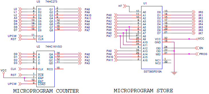
There are two parts (U2 and U3) that together produce the 12-bit microcode address. Only the lowest four bits are in a '161 counter chip and actually count (at each cpu CLK pulse). That means that a stretch of 16 micro-instructions must always end with a jump to another position in the microcode (otherwise the same 16 micro-instructions will be repeated).
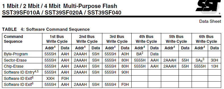
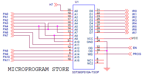
The microcode address is connected to the address bus of the Flash ROM chip U1, together with the flag bit this makes 13 address lines. So why are the unused address lines (A9 -A12) not simply connected to logic 0 (GND) ? That is because we also want to be able to program the Flash chip while it is soldered in the CPU. For programming it, we need to present a certain sequence of commands to the chip, as mentioned in the datasheet:
![]()
We see that the address must be alternated between 0x5555 and 0x2AAA in order to program bytes or to erase the chip. By connecting A9 - A12 to A5 - A8, as shown above, it is possible to generate these addresses although only 13 address bits are actually used.
At the right side of the Flash chip you see that it delivers the eight microcode bits IR0 - IR7. It also shows the two signals EN and PROG, that are connected to pins of the CPU to enable flash programming (but on the CLOCK pcb, EN is called US_OE, and PROG is called US_WR).
The shown connection of the Flash chip is the way it was connected on the NAC pcb and on the first version of the 1x1" cpu. However, the TSOP version has another pinout than the DIP version, and the cpu pcb had to be redesigned with a correct flash pinout. The flash had to be turned 180 degrees, and it was impossible to connect all traces again. Therefore, the connection of the address bus was changed a little:
![]()
Address connection looks a bit messy but the effect is the same. In the following screenshot you can see how flash pins 13 - 16 are connected to alternate signals :
![]()
MICRO-INSTRUCTION DECODE
![]()
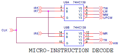
This decoder determines the data routing for each cycle.
The lower HC139 half will select which device can place it's contents on the databus. There are only two: MR (memory-read) will let the external memory (or input port) place something on the bus (From which address that information comes is decided by the address generation circuit, discussed above). The TR (Temp-read) will let the B register place its contents on the databus. The HW (H-register-write) signal is also on the lower multiplexer but this will load the H register from the lower address bus (described in address generation). The upper multiplexer might have been a better place to connect the HW signal, but that was full.
The upper HC139 will select which device is written:
- TW will write the databus contents to the B register
- LW will write the databus contents to the L register
- MW will write the databus contents to external memory (or output port)
- UPCW will write the B register and the upper four bits of the L register to the micro-program counter. The current microcode version uses only 256 addresses, the bits loaded from the L register are always 0 (the output of L can be forced to 0 by making IR4 high).
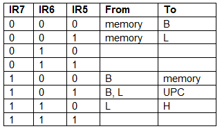
The decoder gives us the following routing options, based on the values of IR5, IR6 and IR7:
![]()
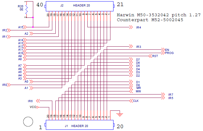
CPU EXTERNAL CONNECTIONS![]()
This last part of the schematic show the connections to the outside world. Pins 1 and 40 are not actually connected on the pcb, a little wire is needed (as explained in THIS log). If you have read all previous logs, there will be no surprises here. Not shown on any of these schematic sections is that there are also 4 decoupling capacitors on the pcb.
This is the end of the grand tour through the little CPU !
-
Clock application pcb
10/20/2018 at 14:43 • 0 commentsCPU demo: CLOCK
Since yesterday, the clock application is fully working. It includes button functions for setting the clock to the current time. The browser based Javascript assembler was updated again, it will now show today's clock source code when you open the page.
An "Assembler code manual" was made and put in the files section today.
This log will discuss the pcb that was made for the clock demo.
For the full schematic of the clock application pcb, please refer to the CLK1840.pdf in the files section. The gerber fies are also in the files section.
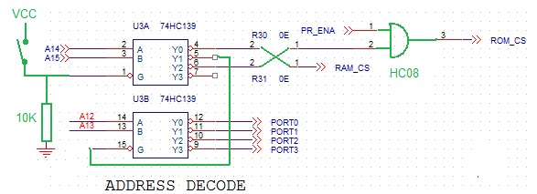
ADDRESS DECODER
The address decoder on the schematic and pcb is this:
![]()
This was designed very quickly before the implications of all design decisions were known. But it has the possibility to swap the address range of ROM and RAM, by leaving R30 and R31 out and cross-connect them. It also shows that when the programming of the application flash is enabled (PR_ENA = 0), the ROM will always be selected. That is needed because for programming the ROM, all 16 address lines must be controllable.
However, this circuit must be changed by modifications on the pcb:
![]()
As you can see in other logs of this project, ROM starts at 0x8000 so the R30-R31 swap must be done. And the I/O ports were not properly decoded, that's also corrected here.
The ROM can be selected by the decoder OR by the PR_ENA signal, so at first sight the HC32 OR gate was OK. Just too bad that these signals are active low, so a HC08 AND gate is needed. I soldered it on top of the the HC32 (the outputs not connected), disconnected pin3 of the HC32, and a short piece of wire did the rest.
And during programming of the microcode or application flash, the Raspberry Pi needs control of the databus. That would become a mess if the Flash ROM or RAM of the clock pcb would also put something on the bus. So, during programming, the switch must be closed to disable the ROM and RAM (In my version, the switch is just a wire with crocodile clips). The Raspberry Pi can however still read or write to/from the application Flash ROM because it can enable it by the PR_ENA line.
For a next version, the switch should be a signal controlled by the RPi.
CPU CLOCK
The cpu clock is a free-running RC oscillator built from a schmitt-trigger port HC132:
![]()
The clock runs at 440kHz but can run a lot faster, that just hasn't been tried yet. For normal operation, the clock must be running, so PR_ENA must be 1 and PR_CLK must be 1. During flash programming, the clock will be stopped by making PR_ENA high, and the RPi can give single (active-low) clock pulses by making PR_CLK high (will give a low pulse on CLK).
There is a small problem with this circuit. When the CPU is single-stepped by the Raspberry Pi, the PR_ENA must be high (otherwise ROM is enabled all the time, see ADDRESS DECODER). But that means that the clock is not properly stopped. The workaround is, that the timing capacitor C2 must be manually shorted during single stepping. Room for improvement !
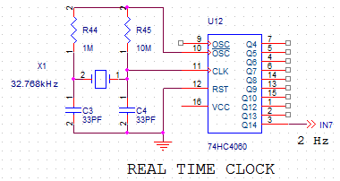
REAL TIME CLOCK
![]()
The real time clock delivers a 2 Hz signal derived from a watch crystal. At first it didn't want to run at the correct frequency. It took me some time, but the solution was simple. The power bypass capacitor for the 4060 was not close enough to the chip (a few cm away). After bypassing VCC directly over the chip, with 100nF, it ran perfect (the schematic shows VCC unconnected, but it certainly is connected on the pcb). The 4060 is the only chip that is SMD (SO16) and mounted on the bottom side. All other chips on this pcb are DIP and mounted on top side.
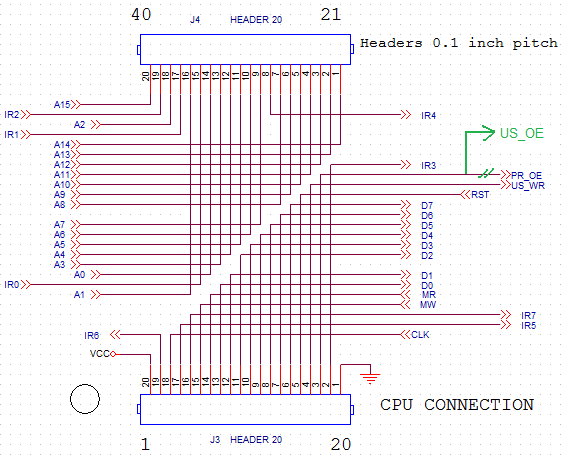
CPU CONNECTION
![]()
Here you see the connection to the "big" NAC (No-ALU-CPU). Two headers are shown, but they are placed at 0.1" distance to form a 2x20 header. One of the pins was connected to PR_OE instead of US_OE. It was corrected with a wire directly to the US_OE signal on the programming connector, and a trace cut at the right position. The smaller, but identical connections to the 1x1" CPU were wired correctly.
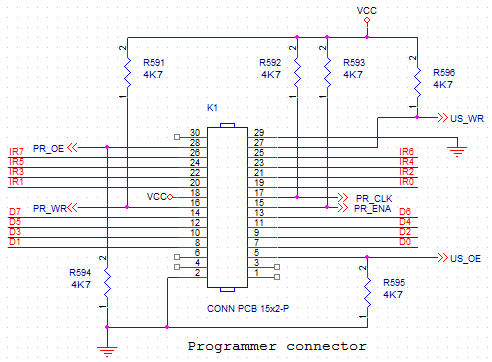
PROGRAMMER CONNECTOR
![]()
Here you see the connection to the programmer. The interface is the same as the one used for the RISC Relay CPU (even the resistor numbers are the same). A small pcb is between this connector and the Raspberry Pi. The small pcb puts the signals at the right pins, and handles conversion between 5V and 3V3.
There are three groups of control signals:
PR_ENA and PR_CLK let the RPi control the CPU clock. The clock can be disabled, and single clock pulses can be given.
US_OE and US_WR (Microstore-output enable and Microstore-write) are used to disable the output of the microcode flash, and give a write pulse to the microcode flash.
PR_OE and PR_WE are used to disable the output of the application flash, and give a write pulse to the application flash.
Bits IR0 up to IR7 are the datalines for writing the microstore flash. Bits D0 up to D7 are the datalines for writing the application flash.
Note that when the Raspberry Pi is not connected, the control signals have pull-up or pull-down resistors to enable normal operation of the CPU.
DISPLAY OUTPUT
![]()
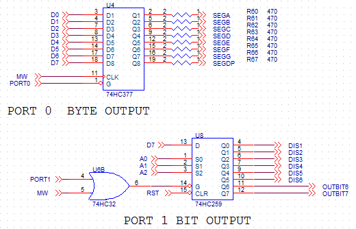
The display output is a standard multiplex system. The six displays are common anode types. Segments are driven by port 0 (0x4000) with 470 Ohms series resistors. The correct digit must be selected by port 1. The IC for port 1 is an addressable latch, that means that the outputs can be written independent from each other, at addresses 0x5000 - 0x5007. The output signals are bit 7 of the databyte that was written.
Note that the outputs are written at the end of the active-low MW pulse. The HC377 has a special input that enables the clock input only when port 0 is selected. The HC259 does not have this, so a HC32 is used, that will only pass the clock when port 1 is selected.
I/O CONNECTOR
The clock pcb can also be used for other applications than a clock ! That's why it has
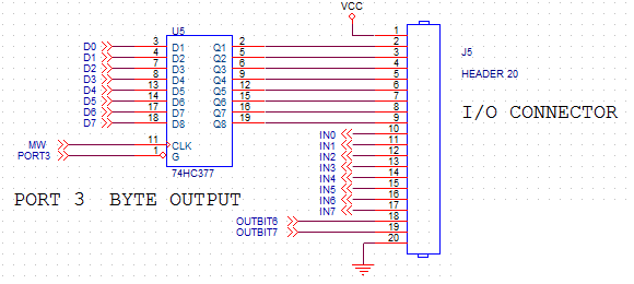
an I/O connector.![]()
The 20 pin I/O connector has 8 bit-addressable inputs on port 2 (but the IN7 signal can not be used because it is connected to the 2Hz RTC). Three of the other inputs are shared with the three control buttons B4, B5 and B6. The 8 bit-addressable inputs have address 0x6000 - 0x6007. After a read from this port, the input bit lands in bit 7 of the accumulator, so it is easy to test the input state with a BRM or BRP instruction. The inputs have an on-board pullup resistor.
The I/O connector has 2 bit addressable outputs from port 1 (OUTBIT6 and OUTBIT7, 0x5006 and 0x5007). The other 6 addressable outputs are used to enable one of the six 7-segment displays.
It has an 8-bit parallel output (port3 at 0x7000) that is not shared with anything.
-
New instructions
10/15/2018 at 14:39 • 1 commentThe new microcode version, with new instructions, is working now !
We now have STACK instructions:
 PUSH Z     ; move a 16-bit value from Z-page to stack

 POP Z      ; move a 16-bit value from stack to Z-page

 CALL label ; push the return address on stack and jump to 16-bit label
            ; 4-byte instruction: opcode, unused, label-lsb, label-msb

 RET        ; load the pc from stack (equivalent to POP PC)
The stack is similar to the 6502 stack, it occupies locations 0100-01FF. There is a single-byte
stack pointer at location 0 in RAM. The stack grows downwards. All items on stack are 16-bit.Note that it would be possible to change the microcode to have a separate stack for return addresses, this would enable a FORTH-style of programming.
Another new instruction is the BYTE-COMPARE instruction:CMPB A,Z ; compare byte in accumulator with byte in zpage ; result A=0x00 when both are equal, A=0x80 when not equalThis works together with the conditional branches BRM and BRP. To make programming easier, the BRM and BRP instructions also have another name from now on: BEQ and BNE, that do exactly what you would expect after a compare instruction:
 BEQ label     ; branch if bytes were equal

 BNE label     ; branch if bytes were not equal
The conditional branches BRM and BRP were originally defined to assist in loop counting. A loop counter could count backwards from a certain value (up to 127). When the count changes from 00 to FF, this FF value can be detected by a BRM (branch if minus) or BRP (branch if positive) instruction.
Back to the byte-compare instruction. How is it possible that it compares two bytes, while there is no ALU or byte-compare chip that can do this function ?
Suppose the two values to compare are XX and YY (hex). The processor needs the reserved RAM region 0x0200-0x02FF for this function.
- It writes 0x80 to 0x02XX
- It writes 0x00 to 0x02YY
- The result is read from 0x02XX.
Ii is easy to see that the result will be 0x80 because that was written to 0x02XX. But if YY is the same as XX, the value at 0x02XX is overwritten by 0x00, so the result is 0x00 when both values are equal ! That is how it works !
The microcode that does this can be seen on the Javascript Assembler page. Scroll down, the byte-compare instruction starts at addres 0x00E0.
-
Success !
10/11/2018 at 20:24 • 2 commentsThe smallest homebrew CPU in the world is working now !
Last week, I spend a few evenings changing the layout, to correct the pinout of the flash chip. Not a really easy task, this is a very crowded (only 2 sided) layout. One week ago, on thursday evening, the new layout was sent to China, and I got the pcb's yesterday. It was assembled today (I had ordered a double set of components the first time, perhaps already having the feeling that the first time would not be right).
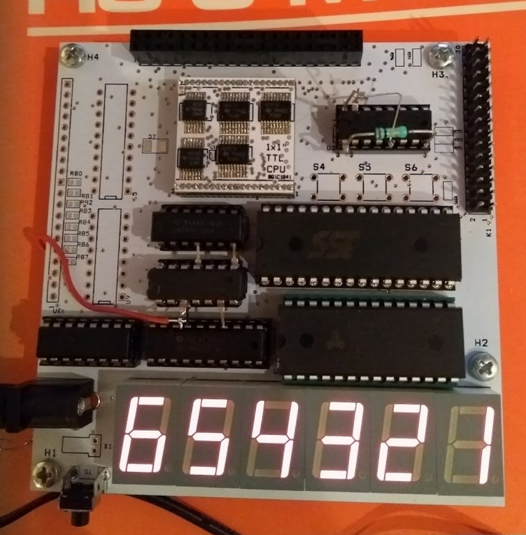
It is now running a simple program, it fills 6 memory locations with the 7-segment values for the digits 1 to 6, and then writes each of them to the multiplexed display in a loop.
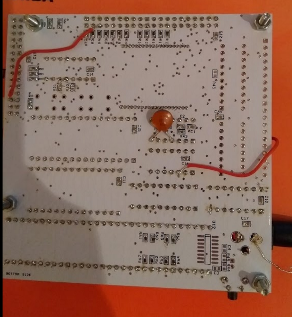
To show that there's nothing hidden, I disconnected the RPi, and I also show the back side of the pcb.
![]()
The display is a bit dim, that's because in the time allotted for each digit, it is only on during 3 instructions and off during 4 instructions. But in reality it is looking better. Perhaps I'll also have to make the resistors a bit lower in value. You can see the program on the Browser-based JS assembler page.
Back side of the pcb:
![]()
I did not work more on the application program yet. After the strike of Murphy, I decided I needed subroutines for the clock program, so I extended the microcode, also making it a bit more dense. The new microcode is now on the Javascript assembler page, but it refused to work on the NAC pcb so it has an error. Therefore, the version that you see on the picture is running with the old microcode.
I will soon update the schematics and gerbers, and describe the application pcb, the NAC, and the modifications.
-
Murphy strikes
09/30/2018 at 09:41 • 0 commentsAfter having the whole system debugged with the NAC pcb, having display multiplexing working, it was time to replace the NAC by the real thing, the 1x1" CPU.
After having corrected a few bad soldered pins, it was still impossible to program the microcode. When reading the flash, all locations returned 0x00. Strange, because unprogrammed locations normally return 0xFF.....
Back to the datasheet......
Well everything that CAN go wrong, WILL go wrong. So if you don't check the datasheet for the pinout.... The pinout for the TSOP is different from the DIP pinout ! Beginner's mistake, I assumed they would be the same without even thinking about it.
So this means re-doing the pcb design and order new PCB's. Today, I will continue to program the 6-digit clock.
-
Debugging struggle
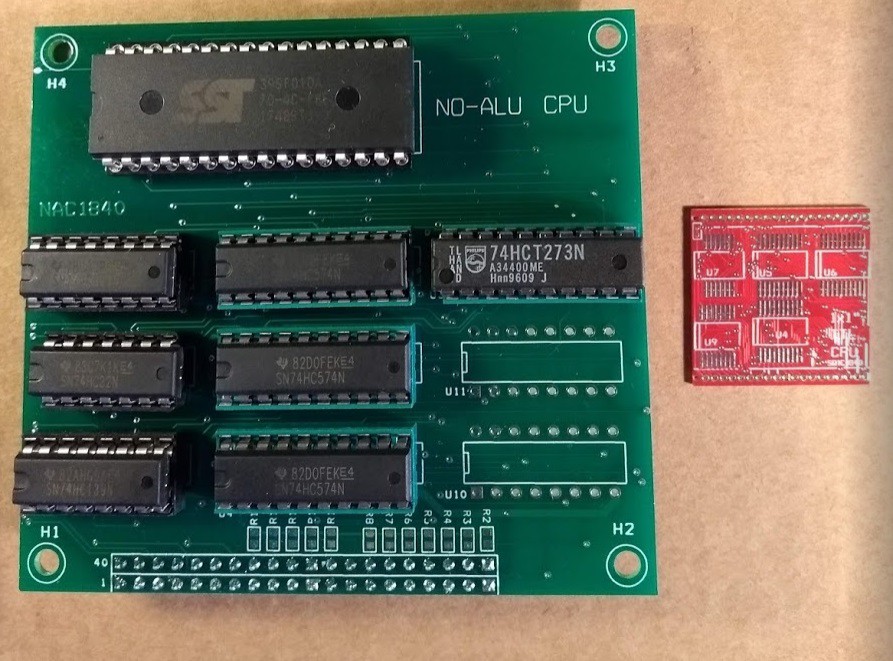
09/28/2018 at 12:20 • 1 commentThe NAC pcb is a bigger version of the square inch pcb. It is intended to make debugging easier. It has two unused footprints, to have room for extra IC's if that would be needed.:
![]()
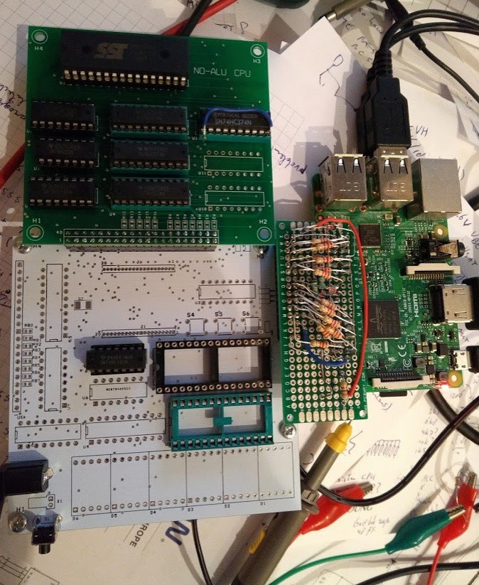
Debugging started with the NAC connected to the application pcb and the Raspbery Pi programmer.
The Raspberry Pi will have two python scripts, one for programming the microcode and one for programming the application code. The last one can also single-step the processor and display the micro-instructions and databus value at each step.
![]()
I corrected a few problems. At this moment, stepping through the microcode works, but only for about 6 micro-instructions after reset. After that, microcode reads as FF... have to investigate....
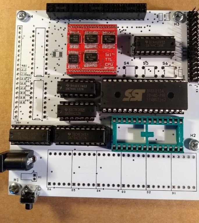
Next picture shows the square inch cpu on the white application pcb. The application pcb contains RAM (empty socket on picture), Flash-ROM, I/O and support functions like clock generation, reset circuit and connecting to the RPi programmer:
![]()
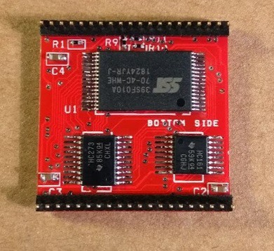
And here is the backside of the CPU, with the 'big' microcode Flash:
![]()
