-
Conclusion
11/23/2018 at 20:50 • 0 commentsThis design is a good demonstration of the tradeoffs in simplicity versus efficiency. The use of negative referenced capacitor supplies allows for easy gate triggering. But there’s a lot of wasted power: several watts of apparent power from the capacitive supply and the sunk gate current (35mA) does no useful work. The control circuits don’t do too bad on efficiency except for the half-watt wasted by R13. Then there’s the footprint: the supply caps are huge and the electrolytic caps, while relatively small, require disproportionate space compared to other components. The snubber components, in this case inductors, require almost as much space as the supply caps.
TRIACs are tricky bastards. Their [relatively] high forward voltage requires heat sinking for all but light loads further increasing cost. Add to this their sensitivity to transients and you have a design with limited versatility.
Contrast this to a MOSFET based design. A single, non-isolated, SMPS powered by dual rectifier sections and an 8-bit MCU. A pair of series, source connected, NFETs comprises each switch. Floating flyback drives switch each via PWM outputs from the MCU. The inherent, high transient immunity of the MOSFETs eliminates the need for snubber networks and the worry & dissipation of confirming the output is off before switching. While a bit more complex than its TRIAC counterpart it is smaller and comparable in cost. Efficiency is very high, with a peak power draw under 500mW. MOSFETs, even back-back for each switch, support much higher loads without thermal management. Not buying it? Check out my timer project - it has all the necessary prerequisites.
The only advantage a TRIAC-based design has is commutating off at zero current. MOSFET designs could implement this using the zero cross detector peripheral available in many MCUs along with a number of efficient sense circuits.
-
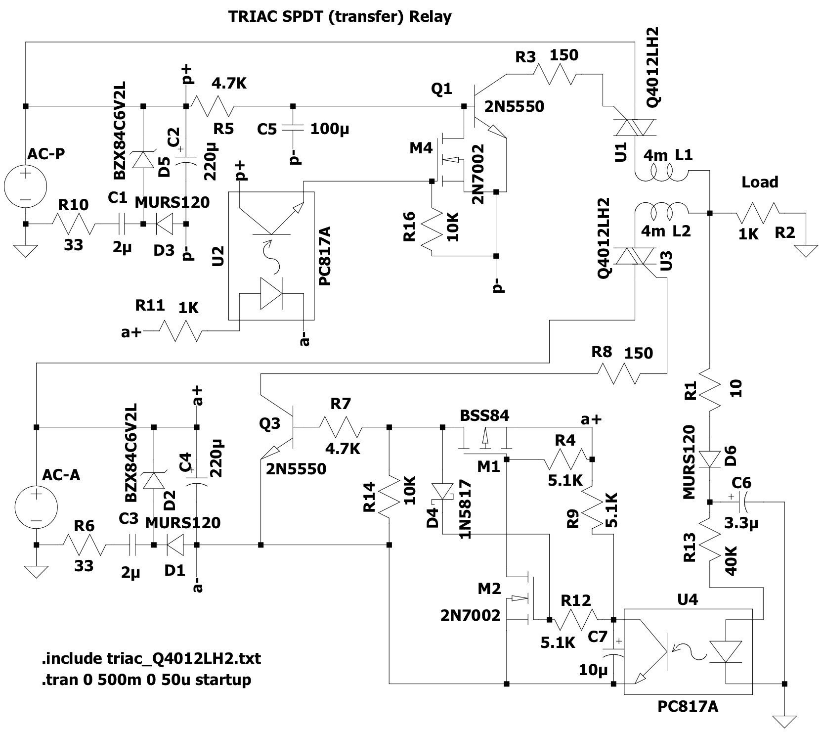
Final Design
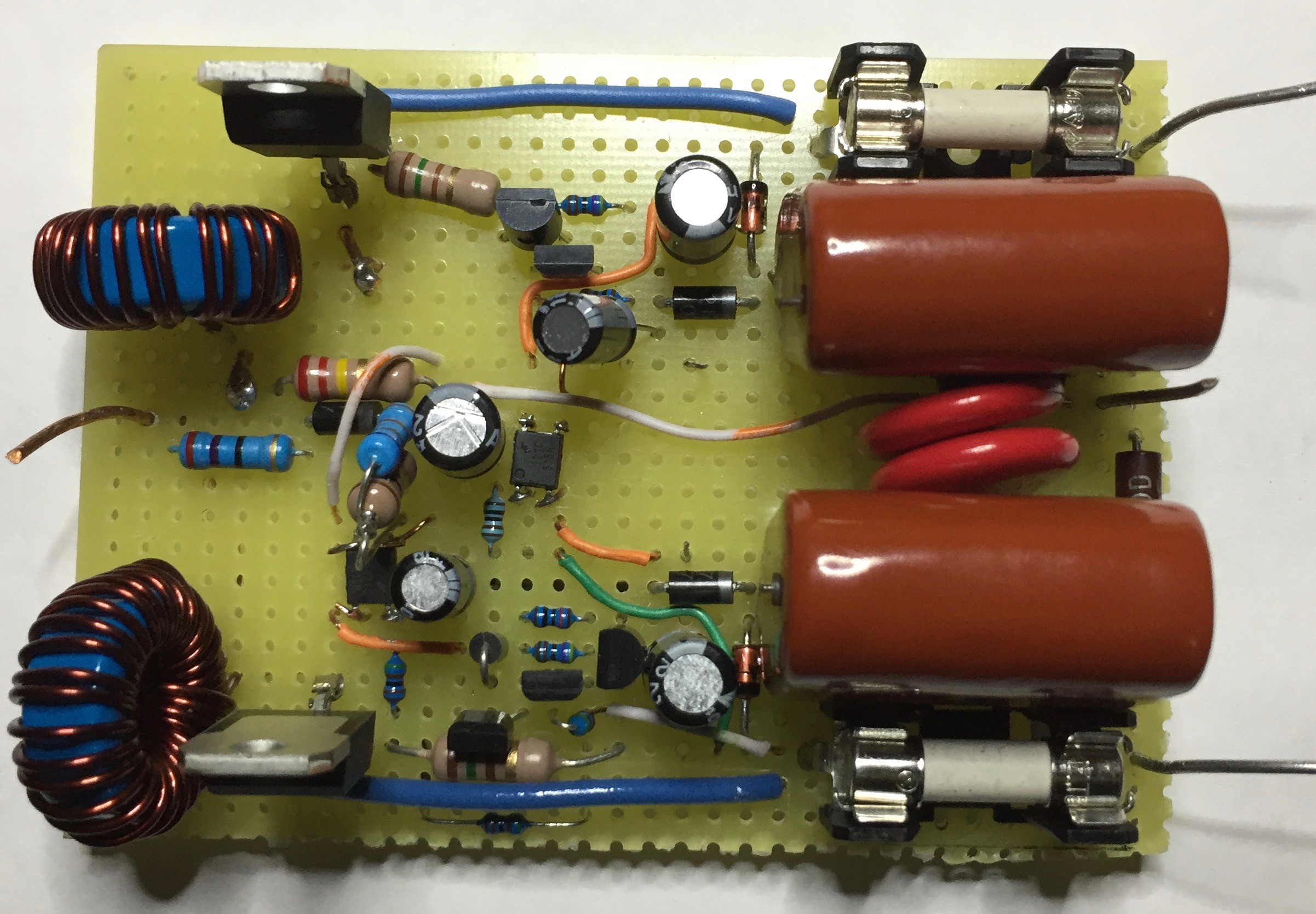
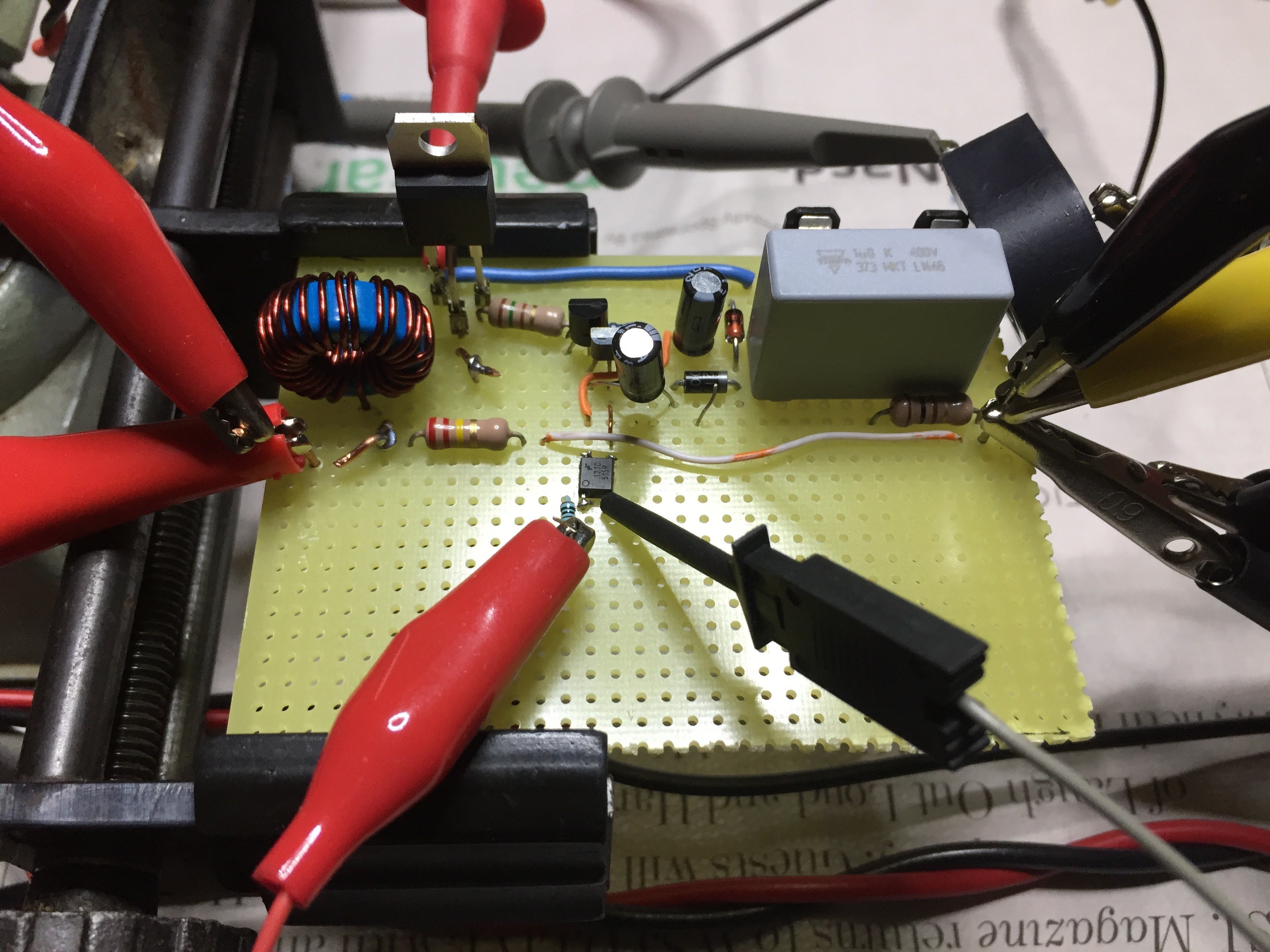
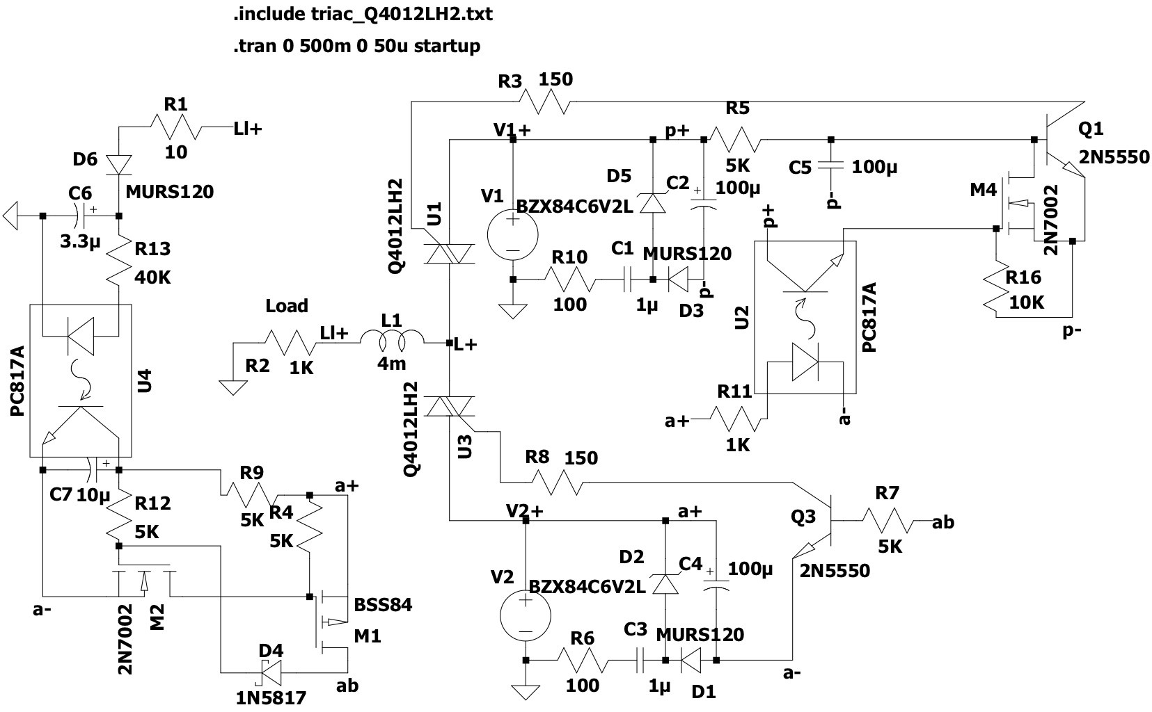
11/23/2018 at 20:47 • 0 commentsAfter building the auxiliary section and testing I’ve called this one done. The spice file is posted as ‘r3’ and the schematic is below. The basic design & theory of operation are as described in the Revision 2 post. The changes are in component values of each of the capacitive supplies to ensure proper operation. Standard gate trigger TRIACs require ~ 35mA to reliably trigger and with the bias required by the control circuits the total current demand is a bit over 40mA.
![]()
A problem with capacitive supplies is that they are current limited based on the time constant. With a half-wave rectifier they must support the supply voltage for a half-wave. At 60Hz this is approximately 8.333mS. With a 6V supply and assuming the AC supply peaks at 170V, the drop across the capacitor is 164V. The basic formula for capacitance is C = (A * s)/V. Rearranging to solve for time: s = (C * V)/A = (.000001 * 164) / .04 = 4.1mS. That’s only half the required time. Increasing the capacitance to 2uF gets it to 8.2mS; close enough.
C1 & C3 were increased to 2uF and R6 & R10 reduced to 33Ω to reduce dissipation at the expense of higher inrush current. Even with these changes the ripple on the auxiliary (a+) supply was large enough that the latch circuit would not reliably function. The more proper way to solve this would have been to redo the latch with BJTs since they are current controlled and in this application would probably work okay. The easy way out was to increase the bulk capacitance of C4 to 220uF which was just enough. I did the same for C2 on the primary to ensure it had some margin too.
With a few exceptions the remainder of the component ratings & tolerances are forgiving. Components rated for 25VDC are fine and currents are less than 10mA. R13 should be rated for at least 3/4W since it is dropping almost the entire AC voltage. It’s value doesn’t need to be exact (to get to a standard value) but limit the current to 10mA and make sure to check the dissipation. C6 should also be rated for 250VDC. All of the MOSFETs should have logic-level gates. M4 won’t be destroyed by C5’s discharge as long as M4’s Rds(on) limits current to its pulse rating. Q1 & Q3 should have an hfe > 100. They will sink about 35mA but the voltage drop is small so TO92 packages are fine. Make sure a low Vf schottky diode is used for D4 to ensure adequate gate voltage for M2. Also C1 and C3 should be rated for 250VAC. The opto-isolators used don’t have any special requirements; Fairchild FODM121 were used for the prototype.
If you build this be sure to fuse both the primary & auxiliary (AC-P, AC-A) inputs. Size according to the load (I used 2A slo-blo). As you can see from the pics on the final build I didn’t do anything special for thermal management which, for my application, wasn’t necessary. However, most TRIACs will have a Vf of ~ 1V and loads drawing more than 500mA will destroy the TRIACs without heat sinking or other thermal management. Last, I also included 250V MOVs across the output side of each fuse to provide additional transient protection (red disks between supply caps).
![]()
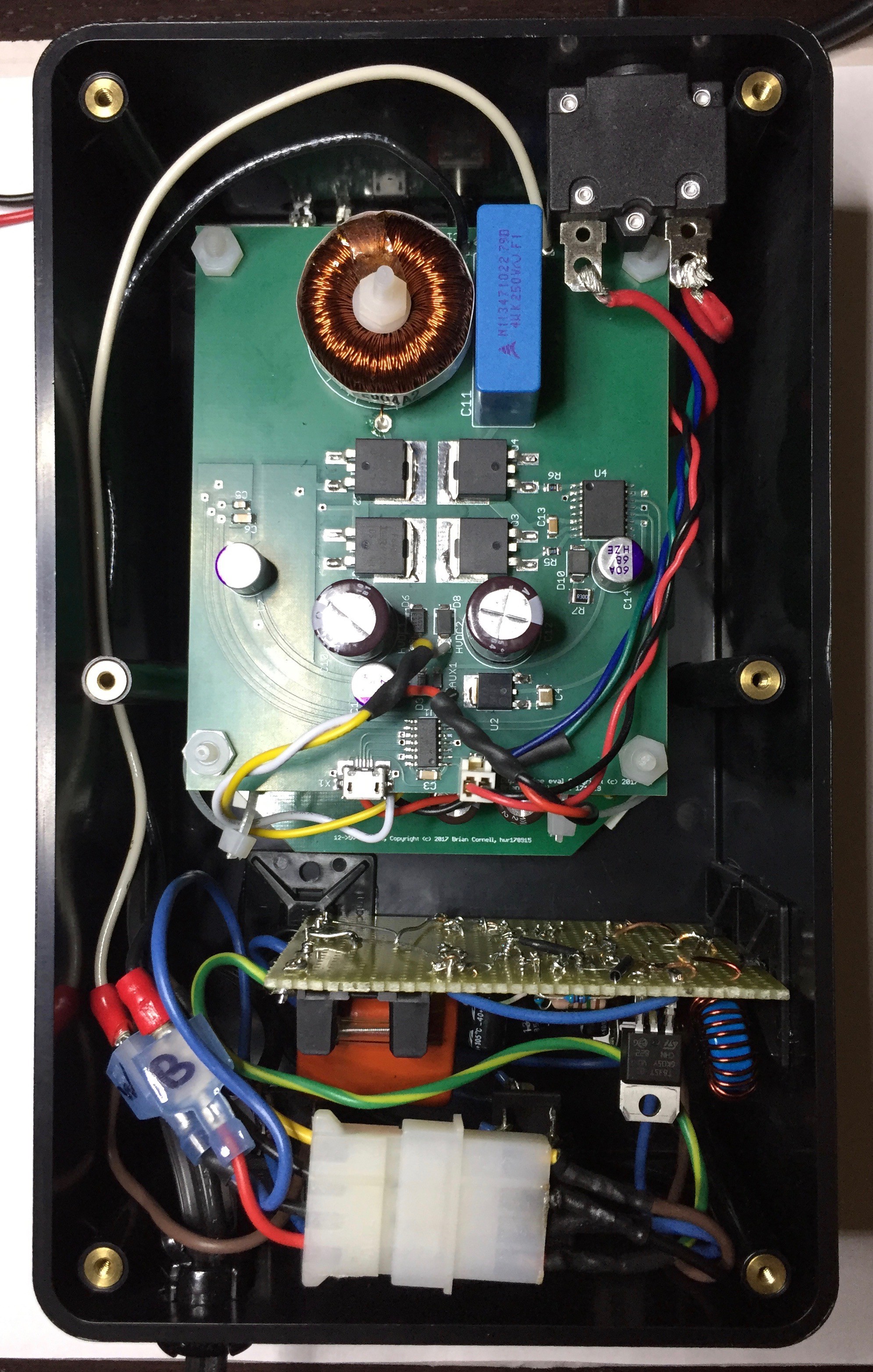
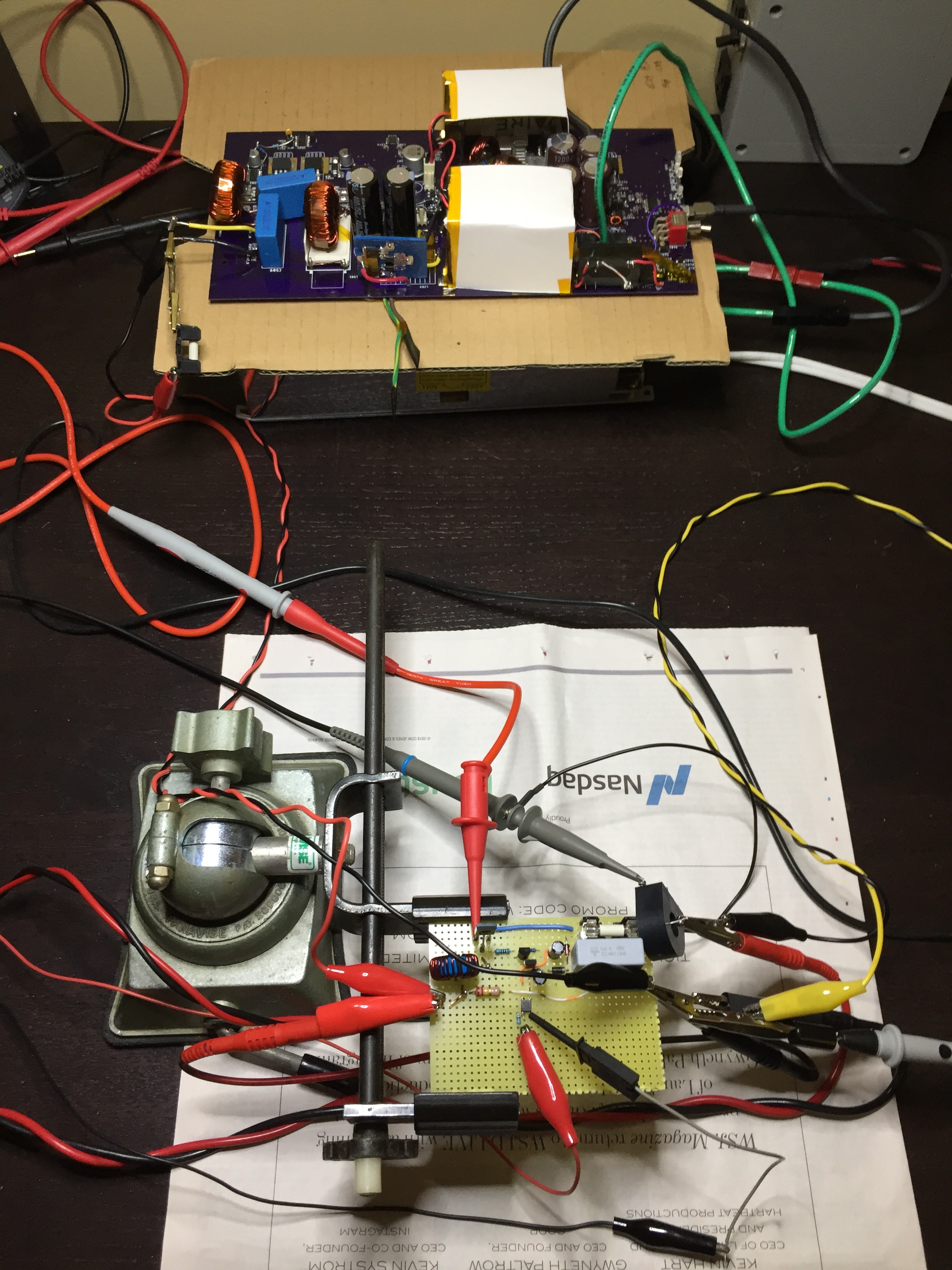
This thing actually works well; I integrated it with my TS50 project to switch between utility & PV AC. Switching time is about 300mS which exceeds the hold-up time of most gadgets so you won’t get uninterrupted operation. You could reduce the value of C7 to shorten but be sure to test.
Back to the capacitive supplies. As shown above this design operates on the edge of what’s possible with 2uF capacitors. Higher currents require larger capacitors, higher apparent power, and diminishing returns. This is important because a TRIAC’s gate bias has a negative temperature coefficient; higher temps=lower gate current, lower temps=higher. This means that at ambients less than 10C (this is a guess, I didn’t test) it may not work reliably but higher temps won’t be a problem.
![]()
-
Revision 2
11/09/2018 at 20:12 • 0 commentsMy first log ended with the word simple; scratch that. After a few rounds of refinement and some in-circuit validation many changes have been made. Before getting to that here are some of the challenges that make this seemingly simple idea complicated.
- TRIACs are susceptible to false turn-ons due to transients (high dv/dt) and can be difficult to turn off reliably depending on power factor and the associated dv/dt(c) & di/dt(c) (c=commutating). Understanding the load is very important.
- RC snubber networks are typically used to reduce dv/dt & di/dt in both commutating & transient situations. This design places opposing, out-of-phase voltages on each side of the TRIAC. These waveforms could also be of slightly different frequencies and peak-peak voltages. The snubber network, typically placed across MT1 & 2, would, in relative terms, have a high apparent power value and require larger wattage components. And while of small value, would also inject some harmonic energy back to the power source.
- Without a snubber network the TRIAC is much more susceptible to false turn-ons - catastrophic and potentially dangerous in this application.
- The circuit must be designed & tested with the type of load it will support. Reactive loads, particularly inductive, have poor power factors and hence high dv/dt(c). This design is intended primarily for resistive and SMPS loads < 100W.
- The control circuit must ensure that both TRIACs are not on at the same time and that there is a sufficient time gap between commutating events to ensure the TRIAC is off.
To elaborate on the last point, I labeled this project as a transfer switch but that is a bit of a misnomer. It does not function like those found in robust UPS' or other standby power systems. This is a stand-alone switch that has no control over the AC sources it is connected to and cannot synchronize voltage, frequency, and phase. Note also that if inductive loads will be controlled the di/dt(c) and peak current at turn-on could be very high - multiples of the load's rated starting current depending on where the core was on its B-H loop during the switching event.
Taking the above into consideration I built the primary half of the circuit based on the original spice file. Note the fuse (500mA, fast): very important to avoid catastrophe. I started with a sensitive gate 2N6073B TRIAC from Littelfuse rated at 400VAC.
![]()
The optoisolator control circuit is in the bottom center and for testing is controlled with a switch & bench supply. Note the TRIAC (upper left) is mounted in a make-shift socket in anticipation of casualties.
No snubber was used and it was fairly easy to induce false turn-ons. While I couldn't add a conventional snubber I did add a 4mH inductor between the TRIAC MT2 pin and the output. The core is high permeability (TDK #B64290L0045X038, N=29, 20AWG) so it saturates at low current and doesn't materially interfere with the load's current waveform. What it does do is provide a small time delay at zero crossing and reduces the initial di/dt. This improved transient immunity but I was still able to induce false turn-ons.
![]()
The 2N6073B was swapped for a T835T-8I from ST Electronics. This TRIAC is rated for 8A and 800VAC and requires a much higher trigger current of ~ 35mA. A huge benefit of a standard gate, higher voltage / current rated TRIAC is much better dv/dt immunity. This is because of the internal channel construction and the addition of resistors in the substrate to drain transient energy away from the gate.
While not perfect, it is rated for snubberless operation when operated within the confines of the data sheet. For comparison the T835T-8I's dv/dt(c) > 20V/uS @ 150C while the 2N6073B's maximum is 10V/uS @ 85C.
The picture above shows the T835T-8I installed for testing along with the output inductor. The 220K resistor shunts the output leakage to ground. This TRIAC tested good; I could not induce false turn-ons regardless of power cycle and transients (induced with an isolation transformer).
![]()
The most important static test of the concept required utility AC to the primary input and an auxiliary AC source across the output with the TRIAC off. The AC was cycled on each side independently and simultaneously to verify that, at least under static switching conditions, the TRIAC would not false trigger and that the control circuit didn't induce a spurious turn-on during power-up.
My other main project, the TS350, supplied AC to the output. The neutrals of both were tied together as common. Note the use of fuses at both AC inputs. This testing was successful too.
Here's the revised circuit which is also posted in the files section.
![]()
Power supplies are the same as original. The actual gate drive for both primary & auxiliary is simpler but the control logic is more complicated. I wasn't comfortable relying on RC timing circuits to control the switching mainly over concern for the TRIACs failure to commutate off properly. Instead I use the latch circuit on the left side of the schematic to manage switching. RC timing (C5) is still used to provide delays at power-up.
The latch works as follows. R1, D6, C6, and R13 form a simple half-wave dissipative supply powered by the output (LI+) and drives opto-isolator U4. R1 provides some reduction of in-rush current. The latch consists of U4's transistor, M1, M2, connected C-D-R components. The latch is powered by the auxiliary supply (a+) and drives Q3 (ab) to control the auxiliary gate.
When AC is applied to the auxiliary input the latch is powered. If the output is on, U4 will be biased and pull down the gate of M2 to keep it off. In turn R4 will apply a+ to M1's gate (a PFET) to keep it off.
Simultaneously, the auxiliary supply, a+, is applied to U2 which turns on M4 and removes the drive bias from Q1. TRIAC U1 should commutate off at the next zero current crossing. U4 turns off with the output which allows C7 to charge and when Vgs(th) is reached M2 begins turn-on, pulls down the gate of M1 turning it on. M1 drives Q3 which in turn commutates TRIAC U3 on. D4 maintains bias on M2 irrespective of the output voltage. The latch can only be reset by removing AC from the auxiliary input.
The time delay provided by C7 is necessary to ensure the primary TRIAC is fully off (think storage time with BJTs). If you try to reduce it be sure to verify experimentally using the intended loads.
Next I'll build the auxiliary half of the prototype and test. Perhaps overkill but I will use a second inductor so that each has a buffer against commutating events on the opposing one. At first I'll keep the primary & auxiliary outputs separate to safely evaluate timing.
So a simple SPDT solid-state switch has taken on a life of its own. It's a bit more complicated than I anticipated but it is straightforward. Unfortunately its not that efficient. Each of the capacitive supplies' true power is ~ 400mW but the apparent power is 4W RMS. U4 draws another ~ 1W when biased so the total true power is close to 2W RMS. Why didn't I just use a mechanical relay?
-
LTspice Model
10/10/2018 at 13:29 • 0 commentsThe project picture is the spice schematic. The spice file is also loaded in the files section along with the required TRIAC model.
Concept: The circuit switches between the primary (V1, utility) and alternate (V2) power sources. The load, L+, is powered by the alternate whenever it is energized. Both AC sources must be tied to a common (earth) return.
Operation: identical negative capacitive supplies are used for both the primary & alternate control circuits. The primary's supply consists of D5, C2, D3, C1, and R10. Half-wave rectification & filtering is done by D3 & C2. D5 is a zener shunt to regulate the supply voltage. C1 is the voltage divider and R10 provides current limiting.
Both the primary & alternate TRIACs trigger in quadrants two & three.
Primary source: when the alternate is off, the primary supply biases Q1 to sink current from the gate of U1 and the load is powered from the primary.
Alternate source: when power is applied to the alternate, the opto-coupler, U2, is immediately energized and charges the gate of M4 which turns Q1 off. TRIAC U1 will commutate off at the next current zero-crossing. The time constant of C16 and R16 insert a turn-on/off delay. Note: U2 is required since p+/- & a+/- are operating at different potentials.
Simultaneously, C15 begins charging and Q3 turns on when its base is forward biased. U4 commutates on. The time constant of R7/R1/C15 must be sufficiently greater than R16/C16 to prevent both TRIACs from being on at the same time.
When alternate power is lost, R16/C16 determine the delay before the primary source resumes powering the load.
Conclusion: the initial design is intended to switch loads less than 100W so no heat sinks are required. Snubbers aren't included in the spice model but will be used in the built prototype although the intent is to switch capacitive (SMPS) or light inductive loads.
In simulation, depending on phase/amplitude/timing of the alternate source, you will see a large current spike when the primary TRIAC conducts in the first half-cycle. I've played with this quite a bit and tried snubbers, adjusting phase of the two sources, etc., but I believe this is an anomaly. I'll find out soon enough; prototype is next!
TRIAC Based Transfer Switch
Simple SPDT solid state transfer switch using TRIACs.