Amos
Amos-
Time for a do-over?
06/14/2020 at 20:14 • 0 commentsThere have been a lot of changes in my life since my last update and I haven't touched any of my projects in so long. Since my last update I started, and then abandoned, an Honors year for my degree; accepted a job offer; moved overseas; and now (like most everyone) I am in lockdown for the foreseeable future.
After I finished my degree last year, I enrolled in an Honors program with the intention of starting a research project based on this tangible programming project. Unfortunately (or fortunately) I received a job offer which meant I would have to move overseas, so I put the Honors program on hold while I moved and got myself re-established in a new country.
When I was preparing to move, I tried to organize my electronics stuff, packing the things I thought I would need for the move, and putting everything else into storage. The first few months in my new home I didn't even look at my electronics gear. When I did start to unpack, I realized I had left a couple of vital boxes back in Australia. 8^/ Also, by the time I did start to pull everything out and do an inventory, the COVID lockdown had started. While this technically meant I had more free time, international shipping was broken, so I couldn't reliably order replacement parts - at least not from my preferred (and cheap) suppliers.
Anywho, I have finally set up a small electronics work bench and have most of what I need to continue working on this project. (Yay!) But should I really continue in the direction I was heading? That I am not sure of...
I have been giving quite a bit of thought about how this project works. Currently, there is a main control unit, which queries the attached modules and executes the program represented but those modules. Each module is currently using an ATTiny841, but honestly I am not really making full use of the capabilities of this chip. Each module represents a program statement and may have optional additional modules attached for setting variable values or calculating expressions. The control unit queries these modules, builds up a map of the program and executes the program internally, only sending commands to the modules to blink LEDs to show the status. My plan was to move the execution logic down into the modules and deprecate the need for a control unit.
So I am now re-thinking this whole approach. Do I continue down the path of a control unit and switch to an even lower cost chip for the modules? I could make the modules even cheaper than they are by making them very simple, and add even more functionality to the control unit. Or do I push ahead on moving the smarts of the program execution into the modules and maybe even jump up to a more "powerful" ATMega329PB in the modules? "Smarter" modules would remove the need for a control unit, but then how would I implement output, stepping through the program and other neat features I have planned?
Another problem I need to solve is the connections between modules. While the pogo pins I was trying last year kinda worked, they were very expensive and I was having some issues getting the alignment of the modules correct. I do need to work on cases for the modules which might help with the alignment issues I had, but the cost of the connectors is still too high. I need to look at other solutions here.
So I think I am going to go back to the drawing board and look at the whole system again from top to bottom before I decide whether or not to continue down the path I was heading.
-
Quick update...
08/19/2019 at 15:58 • 0 commentsI have been quite busy with all manner of things in the past few months, but this project has had some love. (Unlike just about every other project I had in my queue...) I am currently working on a build using pogo-pin-style connectors and magnets to hold the blocks together - TBH I'm not sure it is going to work, but I am discovering some other potential options if these connectors are not quite right. I am trying to mock up some case designs to fully test the new connectors and hope to have a proper update for this project in a few days.
Wish me luck! 8^)
-
Refining the focus (some thoughts)
07/05/2019 at 04:08 • 0 commentsAfter some discussions with a few academics this past week, I have decided to work on (re-)defining the focus of this project. I want to make sure I keep the focus as tight as possible, because adding too much to the scope of this project will run the risk of diluting the core purpose. Keep it simple, focussed and to the point. (unlike my writing style!)
With that in mind, I want to redefine the purpose of this project: SPLaT is a simple programming language trainer, aimed primarily at young children and is intended to teach the basics of programming in a tactile manner. As such, the functionality is intended to be quite limited - integer variables only, simple arithmetic, simple loops and if/then/else conditionals. Functions, scoping of variables, advanced input/output functionality, etc. are all outside the scope of this initial project.
I had started to get carried away dreaming up extensions to the project which would allow functions, attaching Arduino-compatible sensors and modules, different input/output modules and so on, but the problem with this is I believe it detracts from the core promise of this as a tool to teach the fundamentals. If it becomes a general purpose programming tool, it loses its differentiation from other, similar general purpose products.
So, SPLaT will be a simple programming language trainer. The number of variables will be deliberately limited, the size of the variables will likewise be limited to 2-digit integers (0 to 99), and input/output will be limited to simply displaying values. If I get that all working, then I can start to think about extending the language, but I really need to keep the focus tight and simple for now.
-
Numbers!
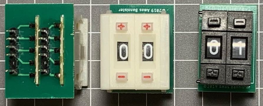
06/02/2019 at 07:25 • 0 commentsSometimes I am too clever for my own good. Or I try to be at least. For numeric input, I had been using BCD thumbwheel switches, which are kinda cool input devices, but they have two drawbacks - one, they are quite large compared to the modules, and two, they can be kinda expensive (and hard to source).
![]()
So I had the brilliant idea of ditching the thumbwheels and using simple "dongles" plugged into the value blocks. All I'd have to do is add some jumper pads to the digit PCBs, solder the jumpers to indicate an appropriate value, solder on the header pins and bingo!
![]()
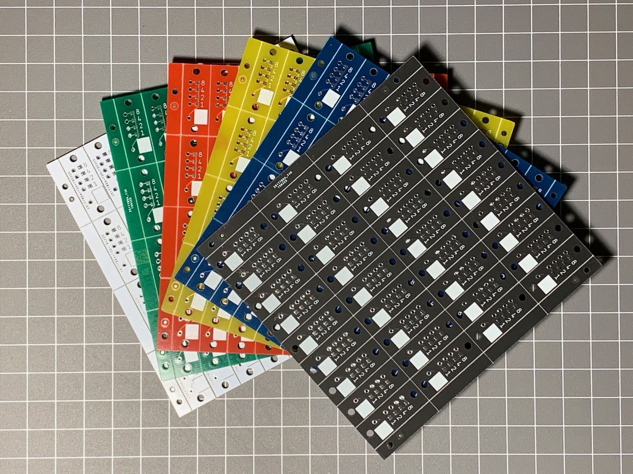
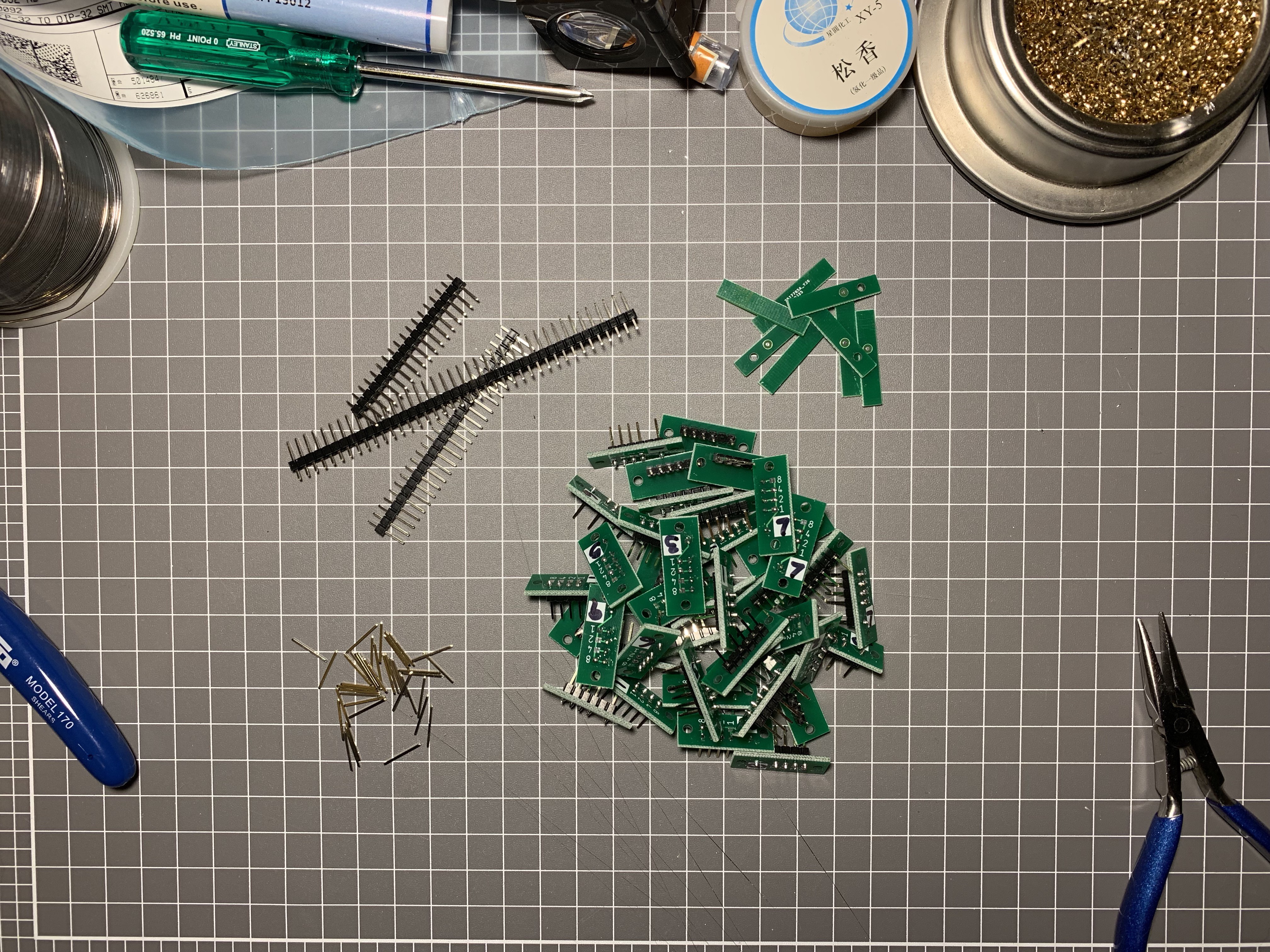
Above are some of the resulting PCBs. If I use values from 0 to 9 for digits, that leaves 10 through 15 as "special" dongles that can represent variables and operators.
And it all works as expected. instead of two-digit values with thumbwheels, I now have a bunch of single digit plugins - to make a two-digit number, just plug in the two digits required. Easy-peasy!
Until you have to solder a bunch of the little suckers! 8^/
![]()
That's just a pile of four of each digit and they took me the better part of two hours to solder the jumpers and headers onto each one. How many will I need? A lot more than this - I don't think this is going to be a suitable solution for hand-manufacture. Then there's the storage and sorting of these little suckers. This prolly isn't going to be a sustainable solution once the prototypes land in the hands of small children.
I have enough thumbwheels for small prototypes, but I think I really do need to find a cheaper, but easier to build, option here.
Does anyone know of a small, cheap, 0-9 input switch that might be worth looking at? Or can you come up with some other (again - cheap) suggestion for entering values?
-
Next revision?
05/27/2019 at 05:36 • 0 commentsI'm about to start work on designing the next iteration of the blocks and modules. I have some (mostly vague) plans for this redesign:
Integrate a value module into some blocks
Variables, Loops, If, Output and some other block types all require at least one value, if not a whole expression to work properly. I think it makes sense to integrate a value module into a program block, which will reduce the number of parts needed to write a program. In order to do this, I think the combined block + value will need to use a microcontroller with more free GPIOs than the ATTiny841.
I really like the '841, but to incorporate a value module I need more GPIOs than are available. I could get around this by including an I2C GPIO extender chip (such as the MCP23008) but that adds complexity and cost. It is probably best to just jump straight to a larger MCU. I'm leaning toward the ATMega328P, or even the ATMega328PB (which has two serial ports instead of one). I have samples of both, so I will do some prototypes to see which works out best...
Revisit the interconnections
Currently the blocks connect to one another using a 4-pin make and female connectors. I think this is fine for prototyping, but it might not be the best solution for a finished product. I need to do some research into other connectors to find something that is cheap and robust enough to be practical. For now I will probably stick with the connectors I am using, but I should start looking sooner rather than later.
The pinout of my connectors is also something I need to look at. The block connections I am happy with - they have VCC, Gnd, Tx, Rx. For block to module connections I have used SDA, SCL, Gnd, and VCC. Grove connectors use SCL, SDA, VCC, Gnd which is quite a different layout. I think it might make sense to standardise on the Grove connector to allow for a wider variety of add-ons.
Finally, I need to look at the value connectors. I am using a modified 6-pin connector, with pin two removed to make the connector polarised. This works, but can be a bit awkward to plug the numeric, variable and operator dongles in at times. So I need to find a better way of plugging values into a block or module.
Form factor
The form factor for the blocks and modules was decreed by the size of the original tiny breadboards I used for my first prototype and the size of the Arduino Pro Mini modules I was using to control the blocks. Now I am using bare chips instead of pre-built devices, I can resize the blocks and modules.
However, I do find the size quite pleasing so far. 30x50mm for the blocks seems like a nice size. The blocks are not too big and not too small for my clumsy hands to manipulate. The variable and value dongles on the other hand are a bit small. 8^/
These blocks and modules will eventually be housed in cases of some description. I would like the cases to be colourful and sturdy, with different functions have a specific colour and shape to allow for quick and easy identification. Smaller PCBs can fit in large cases without problems, but large PCBs limit the smallest size the case can be. I think making the PCBs larger just for sake of making them larger might be a mistake.
The case layout and design may actually inform the layout of the PCBs to an extent. The placement of the connectors, LEDs and value connections all need to be consistent and work with the eventual case design. I should consider mocking up some cases just to get a feel for what I might be working with here.
What else should I consider when designing the next rev?
-
A Name - For Better or Worse...
04/29/2019 at 03:32 • 0 commentsOkay, so after talking to some friends at university, I've decided to call this project SPLaT. That stands for Simple Programming Language Trainer. I'm still not sold on the name to be honest, but if Scratch can survive, why not SPLaT?
I have also thought of another project that can reuse many of the same modules (or at least, very similar modules) which will mean the Tangible Programming moniker will still stand, but more on that later... ;^)
-
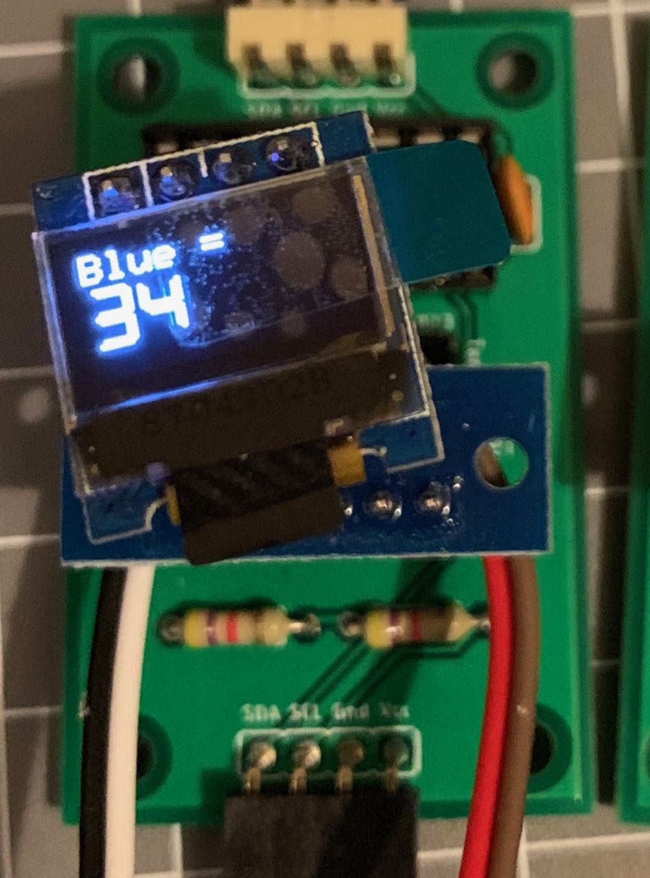
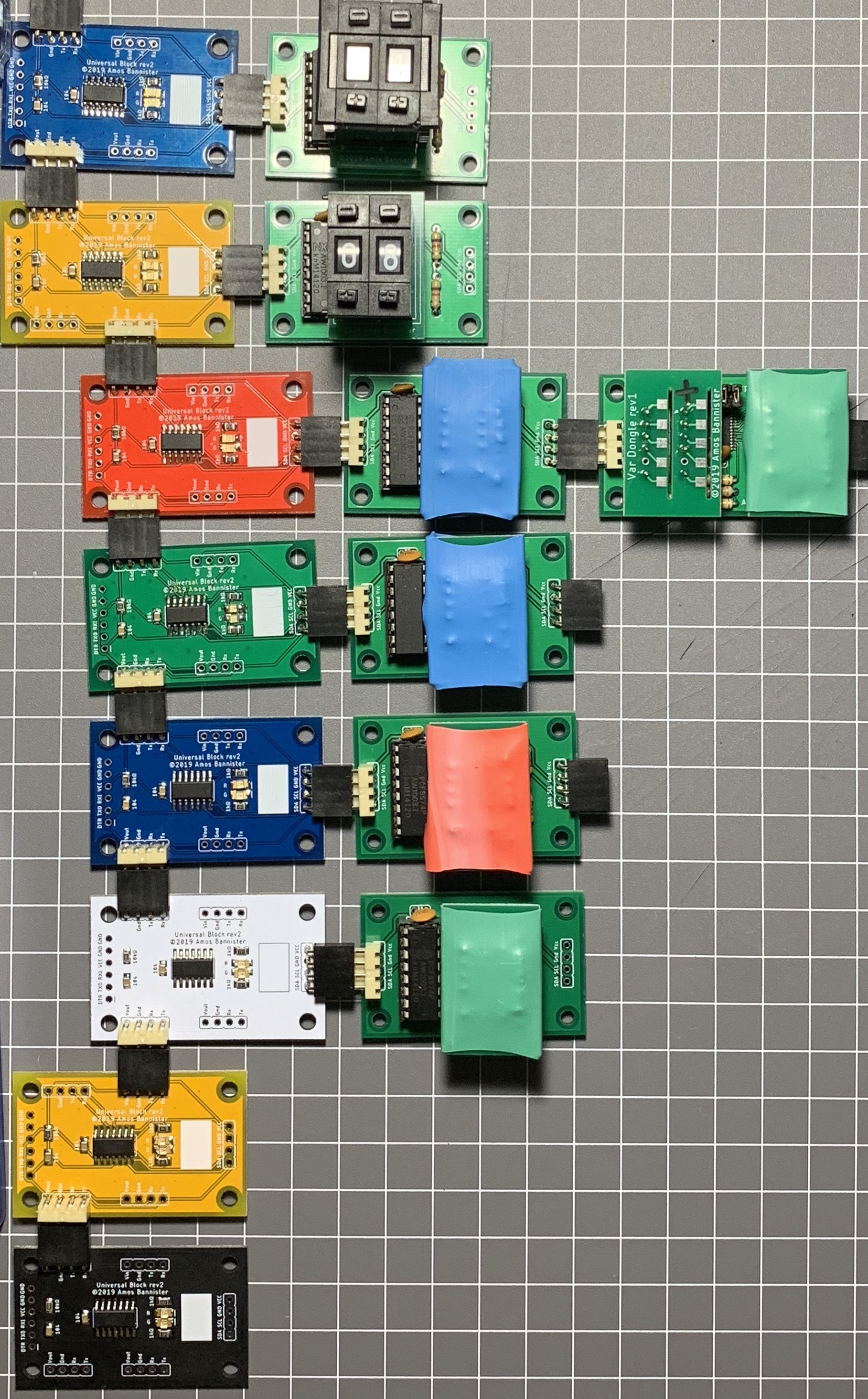
I added a tiny OLED to a block!
04/23/2019 at 11:29 • 0 commentsI still have a few issues to iron out, but I managed to find an OLED library that was small enough to fit on the ATTiny841 and got a small, 0.49" OLED display working on an output block. Now, as the program is running, the output block shows the current value of a variable. I even have enough spare memory to use two different fonts, which I was a pleasant surprise.
![]()
This has highlighted some issues with my power distribution. I really need to work out what is happening with the power. The current set up doesn't quite provide enough power to initialise the OLED on the block, but if I power up the block first with an external power supply, then add the block to the other blocks while it is still powered, then apply power to the master controller, it will work. I think that might be a little too hacky...
I do want to replace the Arduino Uno with a custom board, so maybe that should be the next thing I focus on. I can try to work out the power issues while creating the master controller's board. Or, do I really need a master controller at all? If I can stick a display on individual blocks, the need for a master controller to display the output is reduced. Something for me to think about...
-
I need a name
04/23/2019 at 00:56 • 0 commentsI really should come up with a proper name for this project. Up until now I have mostly referred to this as "Tangible Programming" or "Programmable Blocks". Tangible Programming is closest to what the project is, but it isn't a particularly enticing name. When I wrote my report for the university assignment this came from, I used the name SPLaT (Simple Programming Language Trainer) but I'm not sure about that as a name.
Any ideas? Anyone? What would you call this project?
8^)
-
A brief tour of the latest PCB (plus some discussion of issues)
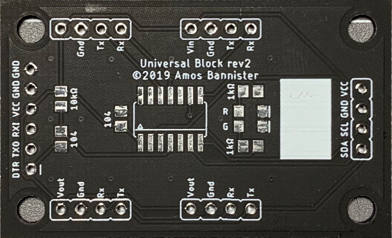
04/19/2019 at 09:01 • 0 commentsI am quite happy with my latest PCBs for this project (thanks JLCPCB!) although they do have some issues. The matte black boards look particularly sexy, although flux residue can be a bit of an issue if not cleaned up.
![]()
I thought it'd be nice to give you a brief tour of the board and talk about some of the things I will most likely be changing for the next revision. The next revision will be some time off, but I am building a wishlist of things to change/add.
A Brief Tour
So let's have a quick look at the current boards:
![]()
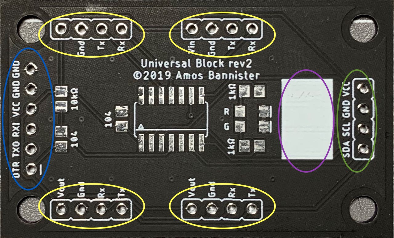
First of all, please ignore the missing Vin at the top left of the board - somehow I managed to delete it before I generated the Gerbers. 8^/
The board is designed to be somewhat flexible, with two incoming serial connections, and two outgoing serial connections. (Highlighted in yellow above.) Both of the ports at the top of the board are connected, as are the two ports at the bottom. This means I can choose to solder the 4-pin connectors in either position, which lets me create blocks that "indent" the code. This can be seen in my favourite demo program (which calculates the Fibonacci sequence) where the yellow LOOP block makes sure the loop contents are nicely indented and the END LOOP block un-indents the code.
![]()
At the right end of the board is a four pin port which is used to connect to other modules. Currently I am using this for value and expression blocks. The port uses I2C, so theoretically any I2C module could be plugged in. (With the appropriate code modifications of course.) That means it might be possible to plug an OLED display directly into a board, or even sensor modules such as temperature, light, or sound sensors, opening up a whole world of new possibilities.
The last port on the board is a programming header. (Circled in blue above) I built a pogo-pin adapter with a USB to FTDI module to program the blocks via this port, and it all seems to work fine.
Lastly, there is a white rectangle at the back of the board where I can label the board's function if required. At the moment I have been able to keep each colour to a a different programming construct and thinking about it, this label might not be needed. For example, yellow boards are being used for LOOP/END LOOP and I will build some yellow variable boards, but the placement of the input/output ports will be enough to distinguish variables from loops.
Other things to note about the boards: There is no power regulation on the board. This was not an oversight - it is by design. The boards draw their power from the input port and the master controller (currently an Arduino Uno, but soon to be a separate custom board) is used to handle the regulation of power. This has allowed me to reduce the parts count and make the boards a bit cheaper to make.
There are two indicator LEDs - one red and one green. The boards can use these to indicate their current execution states, or if they have an error.
And apart from that there is not much else to these boards. K.I.S.S.
Some Issues
Alas, it is not all smooth sailing however...
Flashing the Bootloader
Apart from the missing Vin label, there are a couple of other issues with the board. Starting with the biggie - I forgot to consider how I would flash the bootloader. Oops! While I have the FTDI header, that is not used when flashing the bootloader and setting fuses on the chip. I did manage to get it all working, but it is a bit of a bodge.
To flash a bootloader you need access to an ICSP port. On ATTiny (and ATMega) chips, that means connecting to VCC and Ground (got both of them on the serial ports and the I2C port), MISO, MOSI and SCK (those are TX Out, SCL on the I2C port and RX Out) and the RESET pin. There is a RESET on the FTDI header, but that is connected to the RESET pin via a capacitor, and the ICSP protocol doesn't like that idea. 8^(
I was able to flash the bootloader by connecting the the five broken out pins (basically the outgoing serial port and the SCL pin on the I2C port) and holding a jumper lead on the RESET pin of the ATTiny841 chip. If I slip, the flashing fails, but no damage is done, I just have to try again with steadier hands. As I said, a bit of a bodge, but it is doable.
A minimal fix for this would be to add a breakout for the RESET pin. A slightly better idea might be to include solder pats for an ICSP header underneath the board - that's prolly what I will end up doing.
Wandering LEDs
Another issue relates to the LEDs. Somehow when I was moving components around I moved the LEDs too close to one another. There is enough space that I can solder them without shorting, but it is a bit close for my comfort. I know exactly when I made this mistake and I own it. I just have to be careful of the LEDs shifting while soldering.
Another issue with the placement of the LEDs is where on the board they are. I really didn't give any thought. On the previous revision of the board, the LED (a single, bi-colour jobbie) was plonked down between the two incoming serial ports. That worked well enough, so why did I move it/them? I honestly don't know. I chose to use two discreet LEDs for... reasons... and having made that decision I figured they would fit as nicely between the two ports, so I stuck them behind the ATTiny. Not my brightest idea to be honest.
I think the LEDs would be happier if they were placed at the front of the board, next to the FTDI header. This would also allow me to make some interesting additions to the next revision without causing issues - but more on that idea later...
Future Changes
So I have a small list of changes that should be made for the next revision. Fixing the silkscreen is easy enough. As is moving the LEDs to a smarter location. Adding bare solder pads for an ICSP program header is a solid idea as well. I could then use another pogo-pin jig to flash the boards. If I want to get real fancy I could even make an automated tester/programmer like Unexpected Maker did for his TinyPICO boards! 8^)
The value of extra GPIO pins?
I have come to realise that most of my programming constructs require at least one value to make sense. For example, the variable assignment blocks (Blue, Red and Green in the program above) all need a value and an optional expression to function at all. A loop block needs to know how many times to loop, so that needs a value (or an expression) to function properly. Th output block needs to know what to output, so it also needs a value block to function. This all made me realise that I should probably integrate the value module with the program block. Now that I am using the ATTiny, there is plenty of space on the board for the value modules headers.
Adding a value module to the program board will require a bit of extra thought however. The ATTiny doesn't have enough spare pins for a full value module. For that I need at least eight spare GPIO, or four if I use Charlieplexing. I only have three GPIO pins spare unfortunately. Unless I use the Reset pin as a GPIO, but I think that would require some extra circuitry to allow flashing/programming.
An option might be to use an ATMega328PB. This will give me more than enough GPIO pins, while retaining the dual serial ports of the ATTiny841. As an added bonus it will also give me more memory to play with, which might make connecting to other Arduino-compatible sensors and modules easier...
What about the LEDs?
The LEDs should move, in fact they will have to move if I add the value module to the board. So where exactly should the LEDs move to? These blocks will eventually be housed in cases, so the LEDs should be in a consistent location to make the case design easier. They also need to be in a prominent, viable location. Top-left? Centre-Left? Bottom-Left? Between the input ports? I don't know just yet - this will take a bit of thought...
-
Tracking Down an Annoying Bug
04/14/2019 at 02:02 • 2 commentsWhen I built my first breadboard prototype for my university class, I had a problem where only the first eight blocks would be recognised. When I checked the voltage on each module, I realised that after about eight blocks, the voltage had dropped too low for the Arduino Pro Mini clones to effectively operate. It was actually at around the 11th or 12th module that the Pro Minis would not boot, but I figured that the 9th module didn't have enough power to send or receive serial communications. Luckily my showcase program (the Fibonacci Sequence) only needed eight modules, so I waved the issue off as a power problem and stuck to programs of eight steps or fewer.
With the move to ATTiny841-based blocks I was able to reduce the power requirements considerably, so I ought to be able to have more than eight blocks in a program. Unfortunately my testing showed otherwise. The power was getting through okay, so something else must be at fault here.
I did some testing by tweaking the code. Instead of sending a broadcast message to all modules, I sent an "identify yourself" query to a small handful of select blocks. That showed that I could communicate with the 10th, 11th, 12th blocks with no problems. But if I sent a broadcast query, only the first eight blocks would respond.
Maybe forwarding the broadcast message was failing after eight hops? That didn't seem right, but I through I would try to rule that out. My next test was to send queries to each block individually - i.e. not using a broadcast message. Here is where it started to get weird: Sending 13 ID queries in order (from 0 through 12) still only returned eight results, but the fourth block's response didn't appear. This seemed to indicate to me that timing was an issue, and the timing issue was most likely in the master control unit (MCU), rather than the nodes.
I decided to manually trace the code in the MCU and noticed that I was sending the messages and then clearing the screen in the setup() function and the loop() had no particularly intricate operations during the receipt of the messages. So I moved the code to clear the screen to immediately before the message(s) were sent and bingo! All 13 connected blocks responded and were displayed on screen.
So I can now create programs up to 13 blocks long - any more and I won't be able to display the full program on the tiny screen I am using! As an added bonus, switching the the '841 has reduced the power consumption such that I can power the whole system off a USB power bank. (The Pro Mini modules were too hungry for battery operation and I needed a wall wart to power even four or five modules, let alone eight or more.)
Now that I know what was causing the issue I will revisit the code when I have some spare time and try to make it even faster. I will also look into how I can display longer programs. I am quite relieved that I found this problem and that it was such a simple fix. My biggest fear was that there was a problem with the circuit board, or that there was a more fundamental error in my design.
8^)
Update (16 April 2019)
Today I was showing this project to my Honours supervisor while we discussed my Honours project for next semester. I want to do an Honours project based on the communication protocol I am using - i.e. are there any existing protocols that might be better, or am I on the right track with this protocol? I explained to him this issue and how I fixed it, but I still wasn't 100% certain why it was happening - just that it was a timing issue of some sort. As I said this to him it struck me what the underlying issue was...
When the master control unit (MCU) sends out the broadcast message and then starts the screen clear, the blocks receive the message and start replying immediately. The MCU's serial input buffer starts filling up with the incoming replies while the screen is being cleared. By the time the screen clear has completed and the MCU gets into the main loop and starts checking for incoming data, the serial buffer has filled up and and further data is being dropped. As the MCU reads and processes messages, the buffer gets emptied, but all the blocks have already replied, so no more data will be incoming. When the MCU reaches the end of the buffer, it will be part-way through the last message in the buffer and will be waiting for the rest of the message, which will never come. Also, all the nodes had already sent their responses while the screen was still being cleared, so once the buffer started to be read there would not be any more data incoming to re-fill the buffer - it was already too late.
Moving the screen clear code avoids this problem (for now) as the MCU processes incoming messages fast enough that the serial buffer never fills up.
Several things need to be fixed:
- Even though moving the screen clear code has alleviated this problem, I should still address it, just in case other long-running operations need to happen in the future.
- I am reluctant to add too much overhead to the communications protocol, but maybe some form of ACK/NAK should be implemented? If a node send a message but doesn't get an acknowledgement it might re-send?
- I should definitely include some timeout code while waiting for incoming data - if I receive part of a message but never receive the end, I should send a "retransmit" message to the sending node.
- Maybe I need to look at using interrupts?
It is good to understand what was causing the issue - and hey, this might be good for my Honours project and give me something to do for that. 8^)
Update to the update (a few minutes later...)I forgot to add:
This also explains why I had "random" blocks' messages being dropped when I sent individual queries to all the nodes. I didn't mention this in my initial log, but while hunting for this bug I replaced the single broadcast message with n queries being sent to individual blocks. I knew I was plugging in 13 blocks, so I wrote 13 queries and was surprised to find that I would receive responses from nodes 0 through 3, skipped 4, then 5 through 8, skip 9, etc. I couldn't understand why some blocks were being skipped...
Now I understand what was happening there. While sending the individual messages, blocks would start responding immediately and the buffer filled up. When I had sent all the messages and started the main loop and checking for data, the buffer would be drained, I would reach the end of the buffer which most likely contained half a message. As the buffer was being emptied, more data would be able to be received, but the processing speed given a full buffer must not be quite fast enough to keep the buffer from filling up.
There are some interesting implications to the partial message at the end of the buffer - when the buffer starts being emptied allowing more data to come in, the partial message will eventually be completed by the new data, causing a corrupted message. I definitely need error checking (CRCs?) to ensure that this does not happen.