-
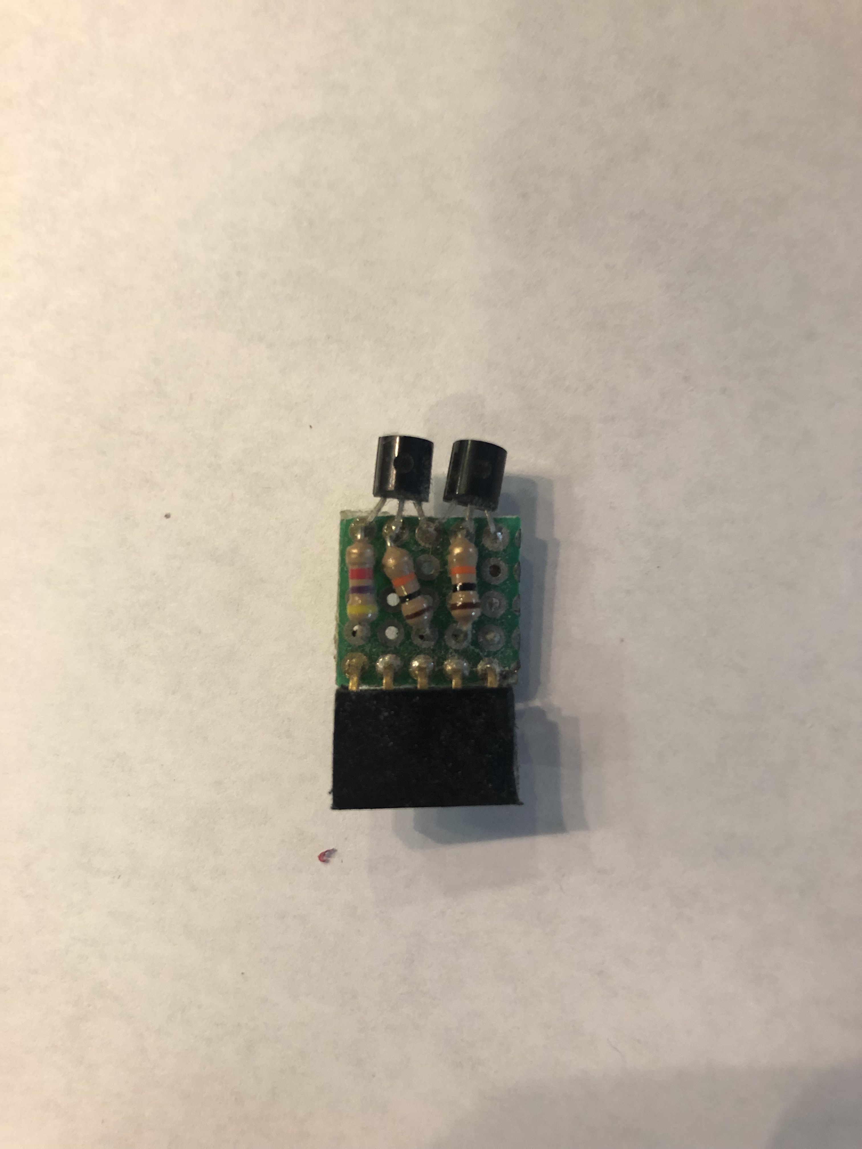
1Constructing the NAND gates.
![]()
First, construct 60 NAND gates, following the given schematic and picture. I did this by cutting out 6x6 hole pieces of prototyping pcb board, and soldering all the components in according to the gate schematic. I then connected MALE pin connectors to the bottom of the gate. This way you can solder all the gates into the board to be connected in the following step. Make sure to test every single gate according to a NAND truth table, BEFORE you solder them onto the board, this will save a lot of headache trouble shooting in the future.
-
2Assemble the board.
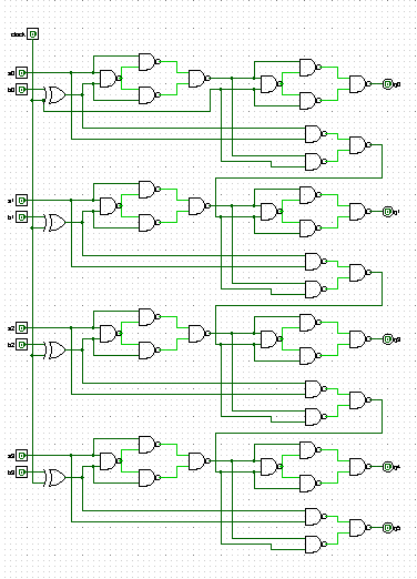
Next, solder all the gates onto the two large prototyping pcb boards. Connect them using lengths of wire according to the schematic.
-
3Troubleshoot
This is the hardest part of the project. You just have to run the simulations in logisim, and test all the connections with a multimeter. As you can tell from the pictures, I had to jack in some more gates after some of gates I soldered in went bad.
-
4Interface
Once the boards are all wired up and working well. You can attach it to your own I/O boards such as switches and LEDs in order to provide an interface for the adder. Your all done!
Discreet Four Bit Adder
This is a discreet four bit adder I designed and constructed using 60 RTL NAND gates.
 Curtis Bucher

 Next, solder all the gates onto the two large prototyping pcb boards. Connect them using lengths of wire according to the schematic.
Discussions
Become a Hackaday.io Member
Create an account to leave a comment. Already have an account? Log In.