I've taken a few swipes at this, but think I finally have it nailed. Here's a tested recipe for 50-Ohm coplanar waveguide traces on OSH Park's 4-layer stackup.
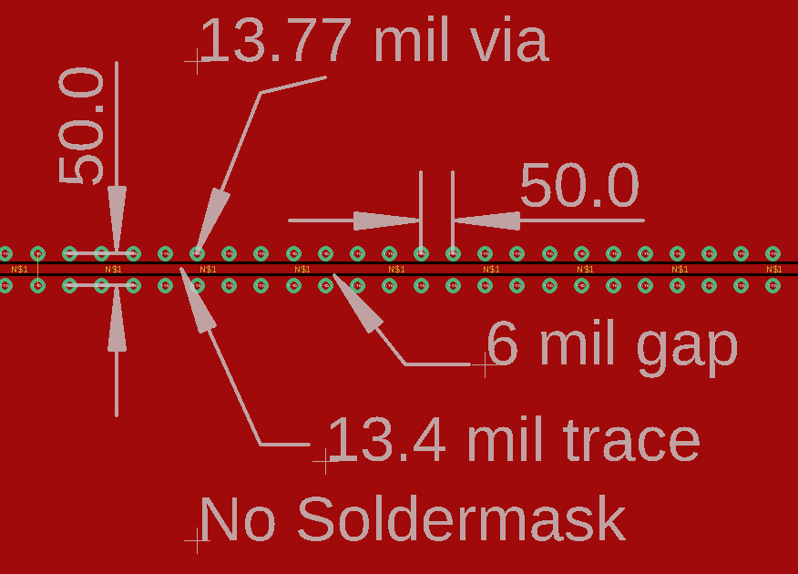
The ground plane for this line is on layer 2, i.e. 6.7 mils below the top layer.
Background
I set the gap to 6 mils somewhat arbitrarily. It's a little bigger than the minimum 5 mil gap in the OSH Park 4-layer design rules, but still small enough to matter for a coplanar waveguide.
To get an estimate of the proper width, I first consulted a number of on-line or application-based calculators. I used an Er value of 3.66 for all calculations. Here is a summary of what they suggest for a 50-Ohm trace:
- Chemandy Electronics: 13.6 mils
- KiCAD PCB Calc: 12.55 mils
- Saturn PCB Toolkit: 13.6 mils
- AppCAD: 12.55 mils
As you can see, there are a couple of different sets of equations floating around.
Sonnet Lite Simulation
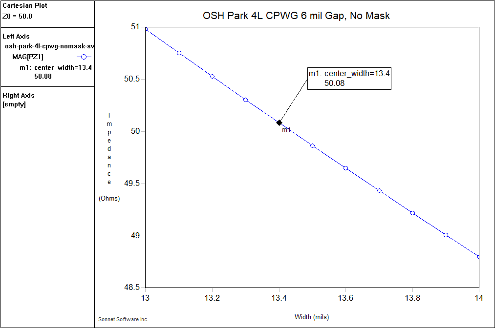
I also ran a test in Sonnet Lite, and produced the following plot of trace impedance vs width. It suggests that 13.4 mils is the correct value.
Test PCBs
I had a batch of three boards made at OSH Park. These each had a 13, 13.5, and 14-mil trace to test. I ignored the 12.55-mil result from some of the calculators, assuming that the model they were using was inappropriate for this structure. I have read that some of the equations used in PCB calculators were originally derived in the context of integrated circuit design, and have difficulties with certain PCB structures, but who knows.
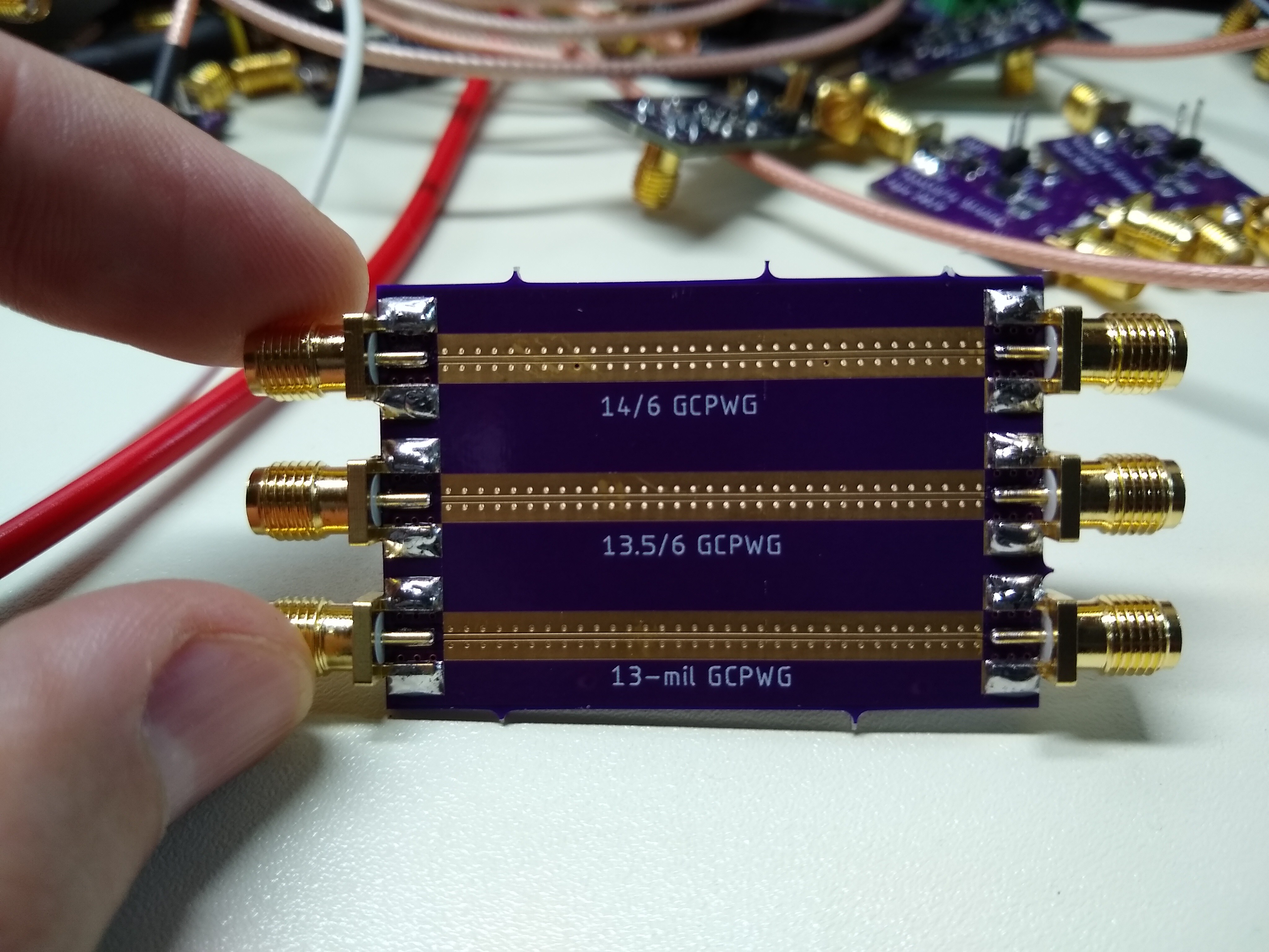
There is no soldermask on the lines, so you have to be careful soldering around them. It is easy to bridge them with solder, and even blobbing some non-bridging solder on there will affect the impedance. I covered the traces with Kapton tape before soldering on the SMA connectors. I removed the tape before testing the impedance.
Measurements
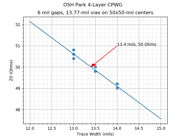
I measured the traces with a Tektronix 11801 sampling scope and SD-24 20 GHz TDR head. You can see the raw 13.5-mil screenshots at the end of this post, but here's a graph summarizing all nine traces. I fit a line to the impedance vs trace width, and it intercepts 50-ohms at a width of 13.4-mils. This is, perhaps not coincidentally, the optimum width suggested by the Sonnet Lite parameter sweep.
You can also get an idea of the deviation you might expect across a larger PCB, maybe on the order of a few tenths of an Ohm. I have no idea what the batch-to-batch variation will be like, and at $24 for a set of three PCBs, I'm not going to gather stats on it at the moment.
What About Soldermask?
So, this is a dilemma. The OSH Park 4-layer stackup uses FR408 substrate with well-defined properties to achieve repeatable high-performance. The dielectric has a known and predictable Er. The soldermask applied over the top does not have a known and predictable Er, and I suspect that the thickness is not terribly well-controlled, either. Soldermask in the gaps of coplanar waveguide will decrease the characteristic impedance of the trace. How large this decrease is depends on the CPWG structure and the nature of the soldermask. On 2-layer PCBS, I have seen the impedance decrease by a few Ohms when soldermask is applied. On the 4-layer version, since the gaps are wider compared to the dielectric thickness, soldermask should have less of an impact.
Then, there's loss. I don't have any data on the loss tangent for soldermask, but I'm guessing it isn't great. But, there's not too much of it involved, I guess, so it may not make a huge difference.
So, the effect is probably "small" but a little unpredictable. On the other hand, without soldermask, the trace is subject to environmental contamination, which can also affect the trace impedance. It's a tough call.
I guess I should make a test board to see what happens.
Screenshots
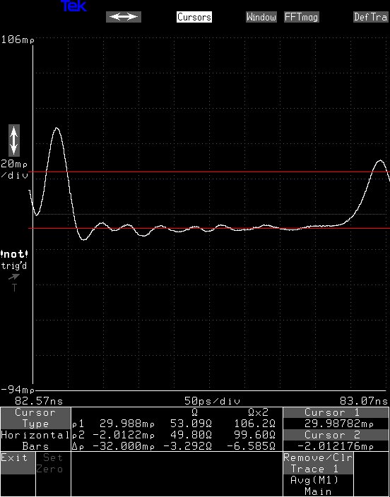
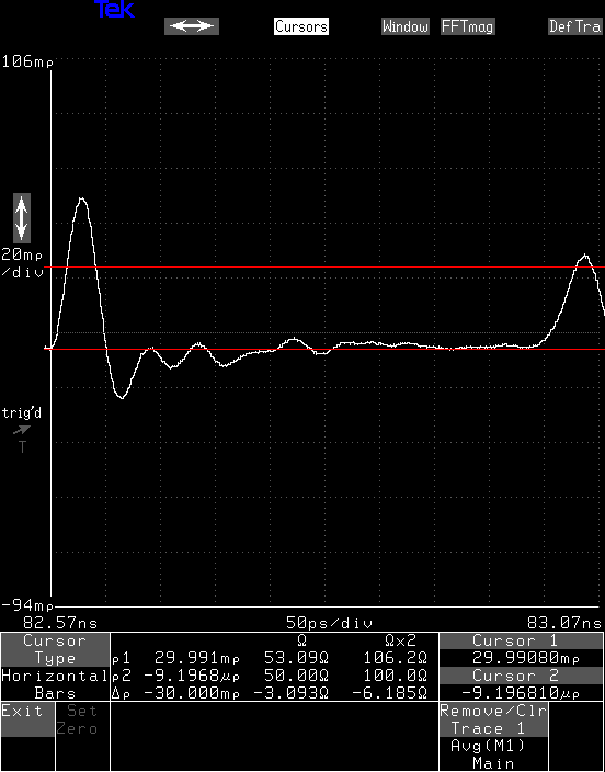
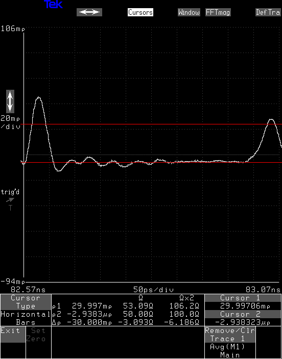
Here are screenshots of the three 13.5-mil traces -- one on each board. You can see where I had to exercise a little judgement in placing the cursor to read off the impedance. I keep thinking I should write some code to grab the raw data off this scope, but in this case, it's probably overkill. So, I should definitely do it.
Another thing. Those inductive impedance bumps on either side are from my SMA connector footprint. They bump up to around 56 Ohms, which didn't look too bad a while ago, but is starting to look like a problem. Maybe time to send out a test PCB with some different footprints.
 Ted Yapo
Discussions
Become a Hackaday.io Member
Create an account to leave a comment. Already have an account? Log In.
It would have been interesting to see the results using a micro-strip line. AppCAD outputs a trace thickness of 13.4 mils for the Osh Park 4 layer board...but perhaps this is purely coincidental. Either way...cool project
Are you sure? yes | no
LOVE this writeup, such good info! Test-driven iteration like this is always super interesting to see.
Are you sure? yes | no
Only just read your article. I have been doing a heap of research on Grounded Coplanar Waveguide (GCPWG) trying to understand the why the S11 performance of a customers PCBs do not seem give expected results on VNA. I have compared various online calculator and free tools against iCD Design Integrity and see much lower impedances when using iCD particularly for cases where (width + 2*gap) > height. This is the case for GPWG using the OSK Park 4-layer build.
The OSH Park 4-layer build does not actually specify the actual pre-preg used between L1/L2 and L3/L4 only the thickness which is given at 6.7mil. Pre-preg will be pressed to give final PCB thickness so the choice of pre-preg will be up to PCB manufacturer unless otherwise requested by the designer. So the Dk between L1 and L2 (same for L4 to L3) could vary from 3.2 @ 1GHz to maybe 3.6 depending of the final resin content.
iCD gives the following impedance results (no solder mask):
w=13.5mil, g=6.0mil, h=6.7mil
Dk=3.2 -> 48.11 ohm
Dk=3.6 -> 45.73 ohm
w=12.5mil, g=6.0mil, h=6.7mil
Dk=3.2 -> 50.20 ohm
Dk=3.6 -> 47.73 ohm
Looking at your plots it would suggest that the Dk is closer to 3.2 and/or the thickness (h) is greater 6.7mil. Etching and plating is going to change the final track width which will move expected results.
Just out of interest what was the finished PCB thickness measured copper to copper? This would allow us to estimate the pre-preg thickness since the other thickness will have less variation.
Are you sure? yes | no
OSH park specifies FR408 for the pre-preg layers and the core:
https://docs.oshpark.com/services/four-layer/
I don't know how iCD is calculating what it's calculating, but Sonnet seems to get this right using a planar method-of-moments simulation, assuming a Dk of 3.66, and the results match what I see on the bench.
Could you be having problems with your connector footprints? If you look at the TDR traces I measured for this board, you can see there would be a bad-looking S11 due to impedance bumps at the connectors, but the TDR can look past that and resolve the impedance of the trace afterwards. Can your VNA do time gating to ignore the connectors?
Are you sure? yes | no
Just to clarify, when I said OSH don’t state prepreg, I meant stating the construction (glass weave and resin content), ie the stated finished thickness for L1/L2 could be 2x3313 or possibly 2x2116 or other builds.
As for the issue I was having with Impedance difference between tool and board turned out the connector footprint was partly to blame.
Are you sure? yes | no
I've been using 12-mil trace widths on OSH Park 4-layer pcbs for my "50-Ohm-impedence" RF lines based on some video I saw and some impedence calculator I found. The good news is that according to your graph, I might be off by a couple of Ohms. The RF radios seems to work just fine (BLE, wifi, LoRaWAN, etc). I hope this is no big deal. But it looks like 13.4 mils might be a better choice. Thanks.
Are you sure? yes | no
It depends on a lot of things. For CPWG, both soldermask and via placement can have a couple of ohms impact. If you replicate the recipe above exactly, you'll probably be close to 50. Adding soldermask will reduce this somewhat, so to compensate, you could make the traces a bit thinner. I don't think I have exact data on this for OSH 4L.
The reality is that a few ohms absolutely doesn't matter for most use cases. Normal coax is 50 +/-2, and for almost everything this is "close enough." In my other project, the 'scope, a few percent reflection shows up as an annoying defect in the step response, so I want to get as close as possible. But, then again, changing the trace width is free, so why not try to hit it exactly.
Are you sure? yes | no
How about devising a method for impedance calibration? E.g. deliberately make a trace just a little bit on a high impedance side, and use a sharpie to add very thin layers of additional dielectric on top, as needed.
Or alternately, make trace a little bit on low impedance side and use very fine sandpaper to remove a little bit of solder mask from the top of it.
Are you sure? yes | no
@salec you could certainly do that for one-off projects. A layer or two of Kapton tape over the top of the trace, plus one of adhesive-backed copper foil would reduce the characteristic impedance, although maybe too much.
For larger traces, like the classic 100-mil microstrip on 1.6 mm FR-4, you can just trim the trace width if necessary.
Are you sure? yes | no
I've been appreciating your posts! Have you ever considered uploading some of the work in progress PCB designs to github? I'm interested in playing with PLL locking on the sampled output waveform, to generate a low frequency sample clock at just the right frequency. My brain is not convinced this is possible, yet I know HP in the '70's had vector voltmeters that did exactly this. My day job doing OS system software will hopefully get a little less consuming this winter, and I might have a little time to play with hardware. To even play in this area, I'd have to first get a functioning sample gate and sample pulse generator to work, an area you have already spent considerable time refining.
Are you sure? yes | no
Sorry I didn't see this comment until now; somehow the email notifications aren't working consistently for me. Anyway, there are some of the early prototype designs on GitHub -- not sure if they went up before or after your comment. Have a look.
https://github.com/tedyapo/sampling-scope-WIP
Are you sure? yes | no
also, if there's something you're interested in, but don't see posted, let me know. I can release things as needed. I made around a hundred small test designs so far for this stuff, and didn't take the time to clean them up enough to be released.
Are you sure? yes | no