All the circuits I am doing for this project are based on one fundamental unit logic gate: DTL invertor/NAND (depending on a number of inputs.
Here is the schematic for 2-input NAND gate:
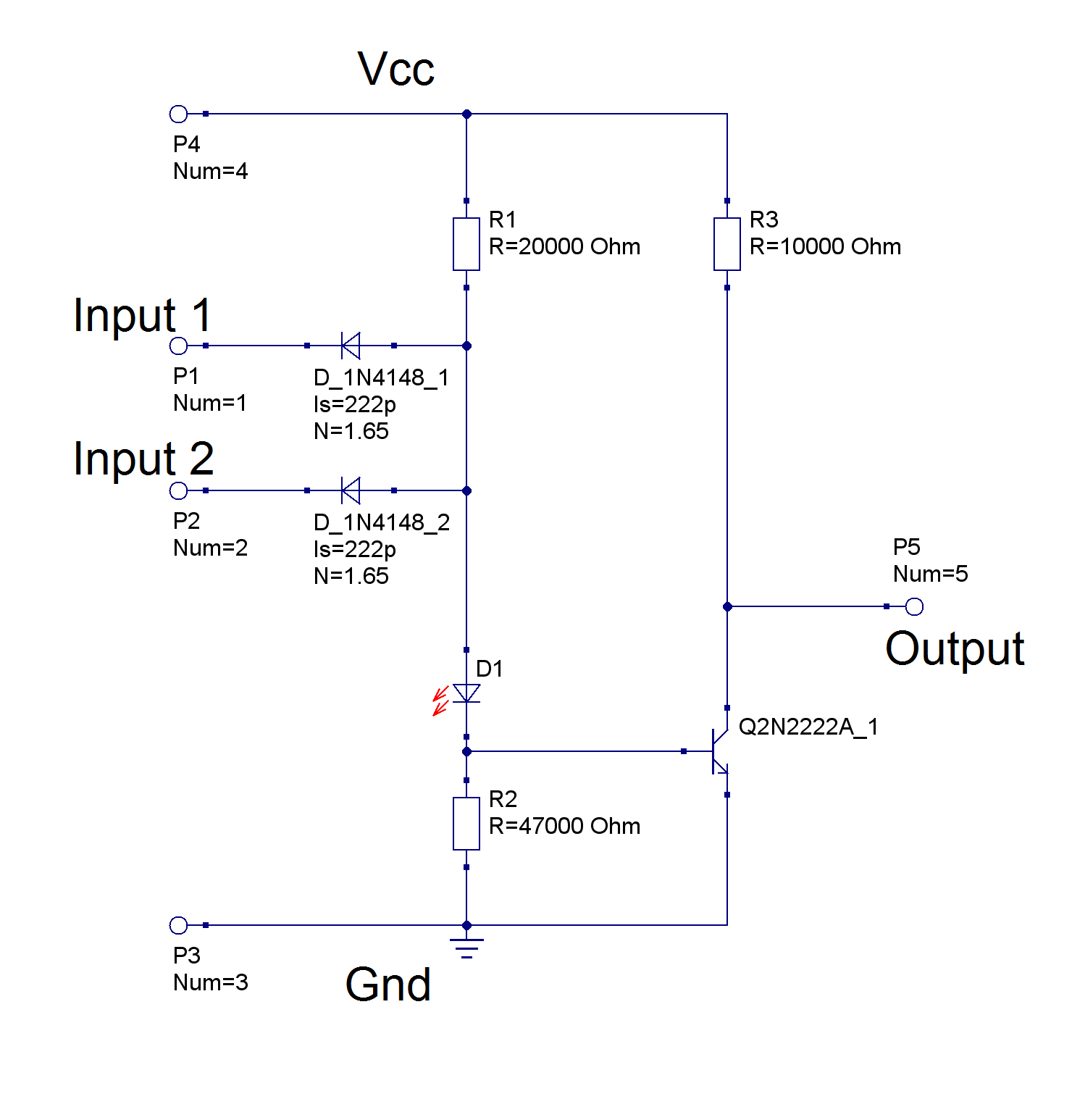
One can make arbitrary number of inputs (within reason) by just changing the number of diodes. By adding additional (inverting) output stage AND gate is done.
With the resistor values shown, the gates are not particularly fast, but on the other hand have a small power consumption. And anyway I have a ton of resistors with these values, so I am using them.
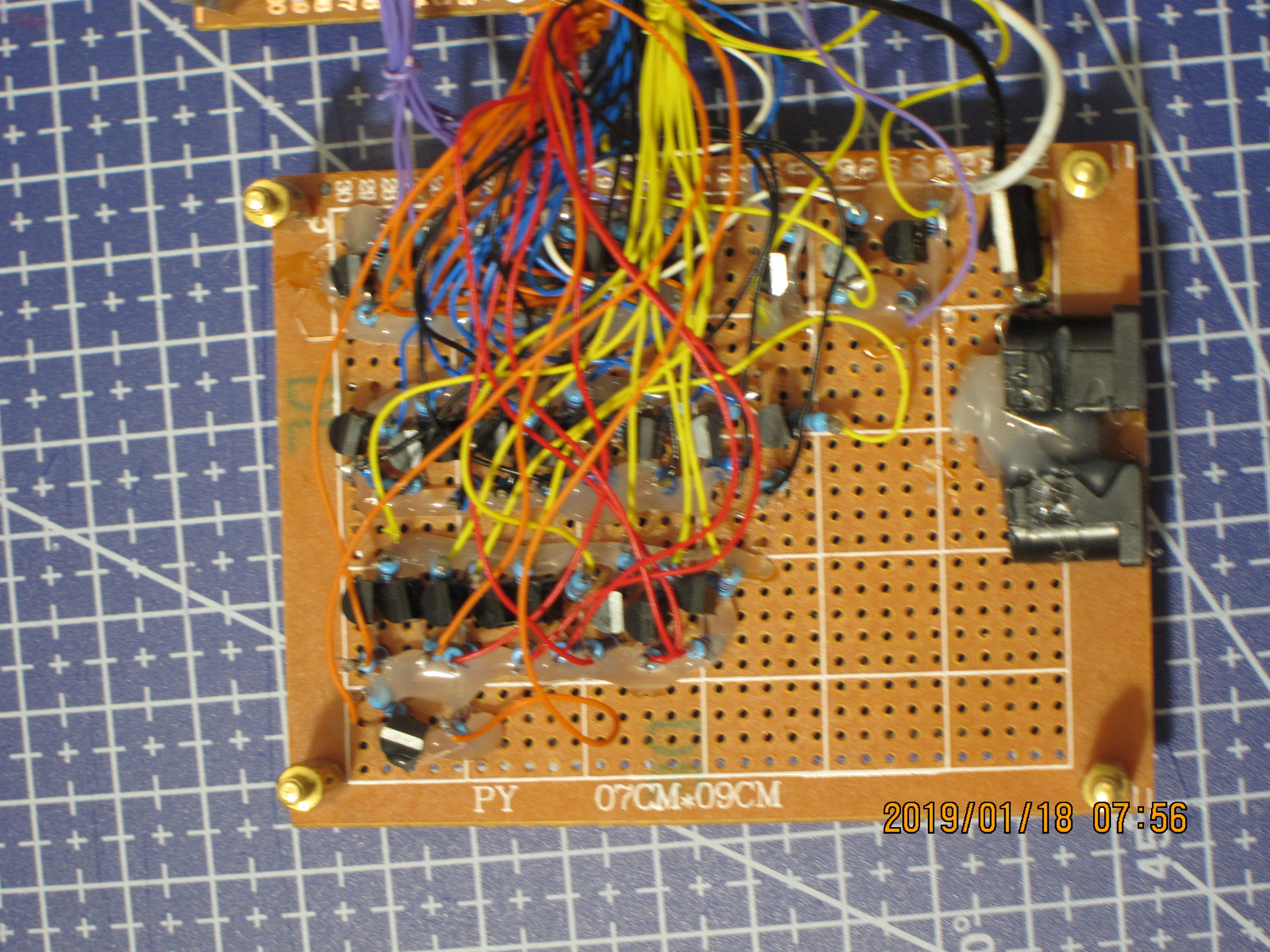
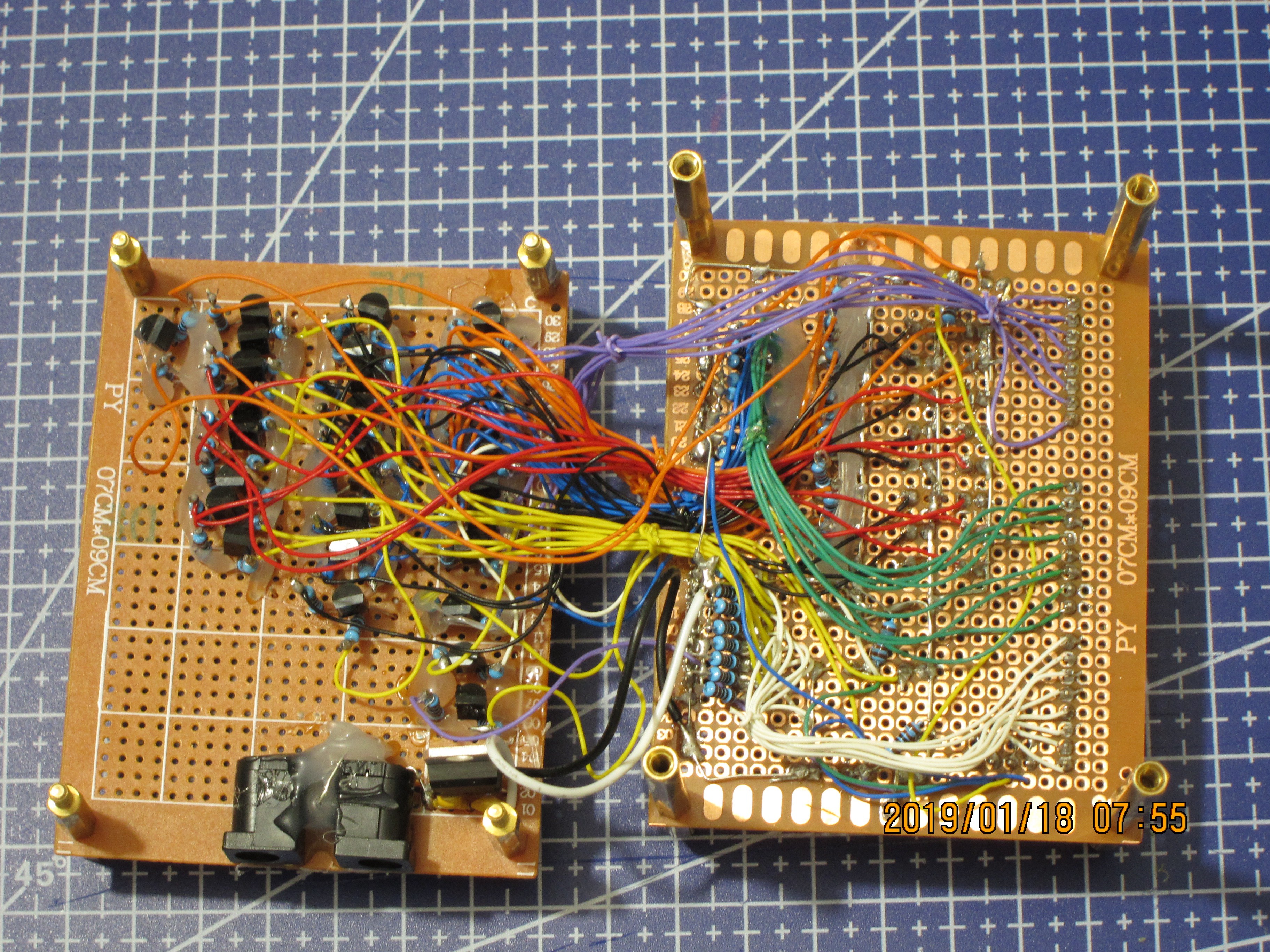
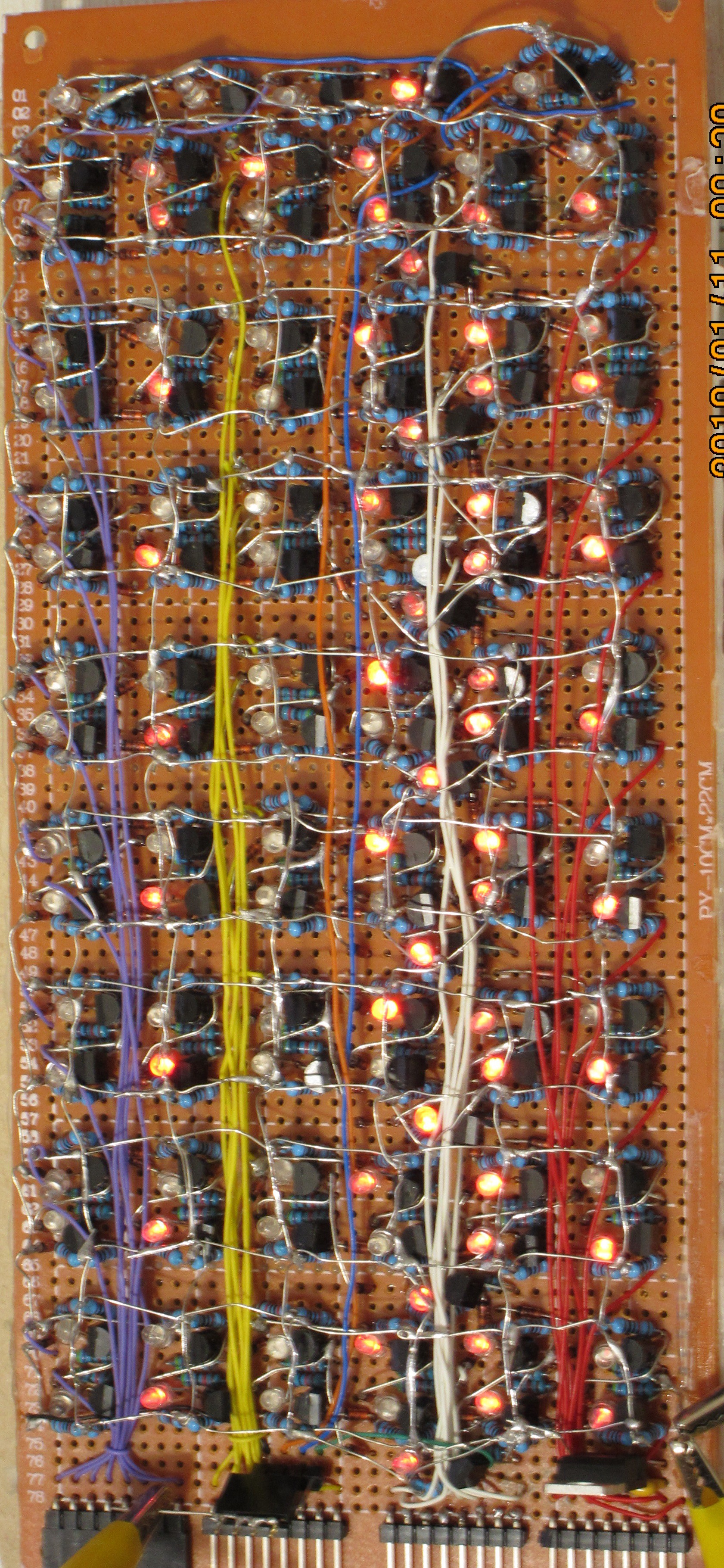
In the course of iterations through the time I came out with circuit layout which can be likened to "semi-cordwood" -- by using 3rd dimension I had achieved much more close packaging, and simplification of wiring, in exchange to reduced repairability. The Vcc and Gnd are on separate planes, with Vcc made as a mesh of inter soldered resistor leads on top of the circuit, and Gnd wires going under it.
On the photo below is the closeup on the Arithmetic board, where details of this construction method could be inferred.
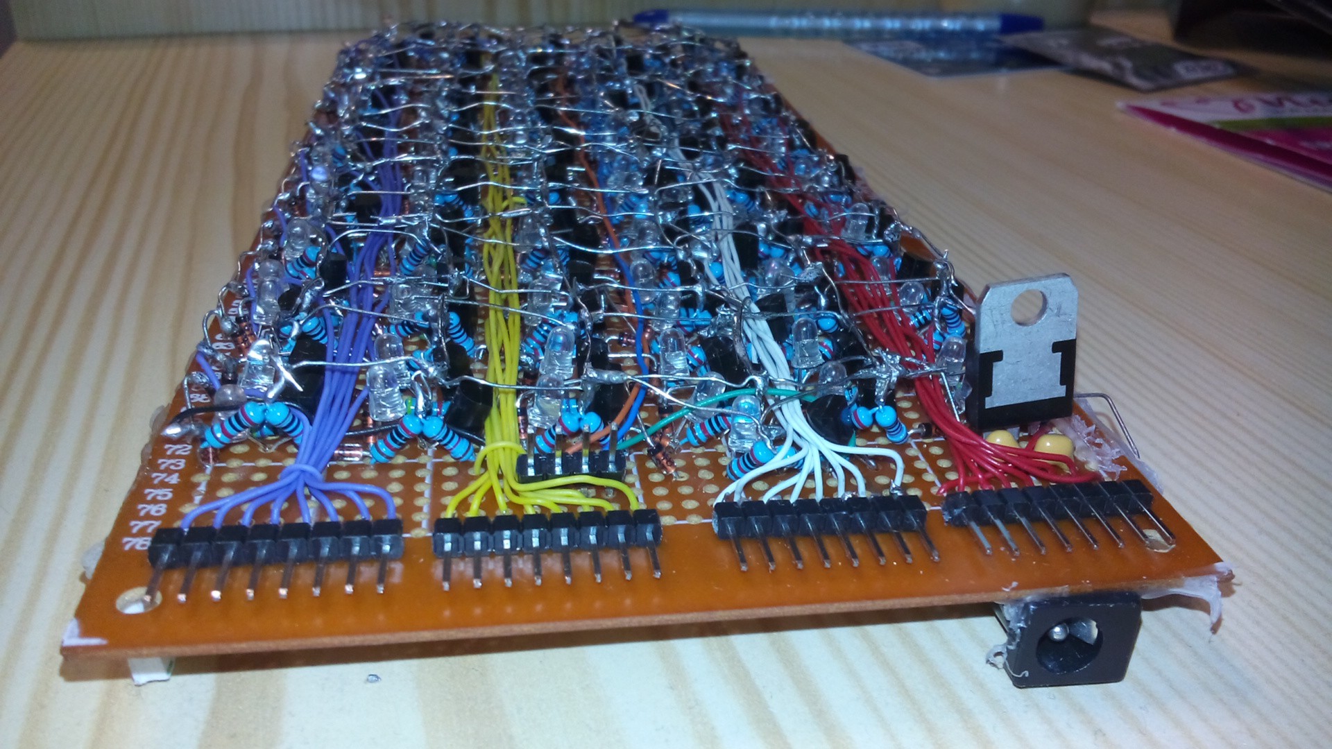
By using component leads as signal pathways and connecting gates directly with them, as well as placing gates more closely and symmetrically, further compactification and reducing number of additional connecting wires is achieved.
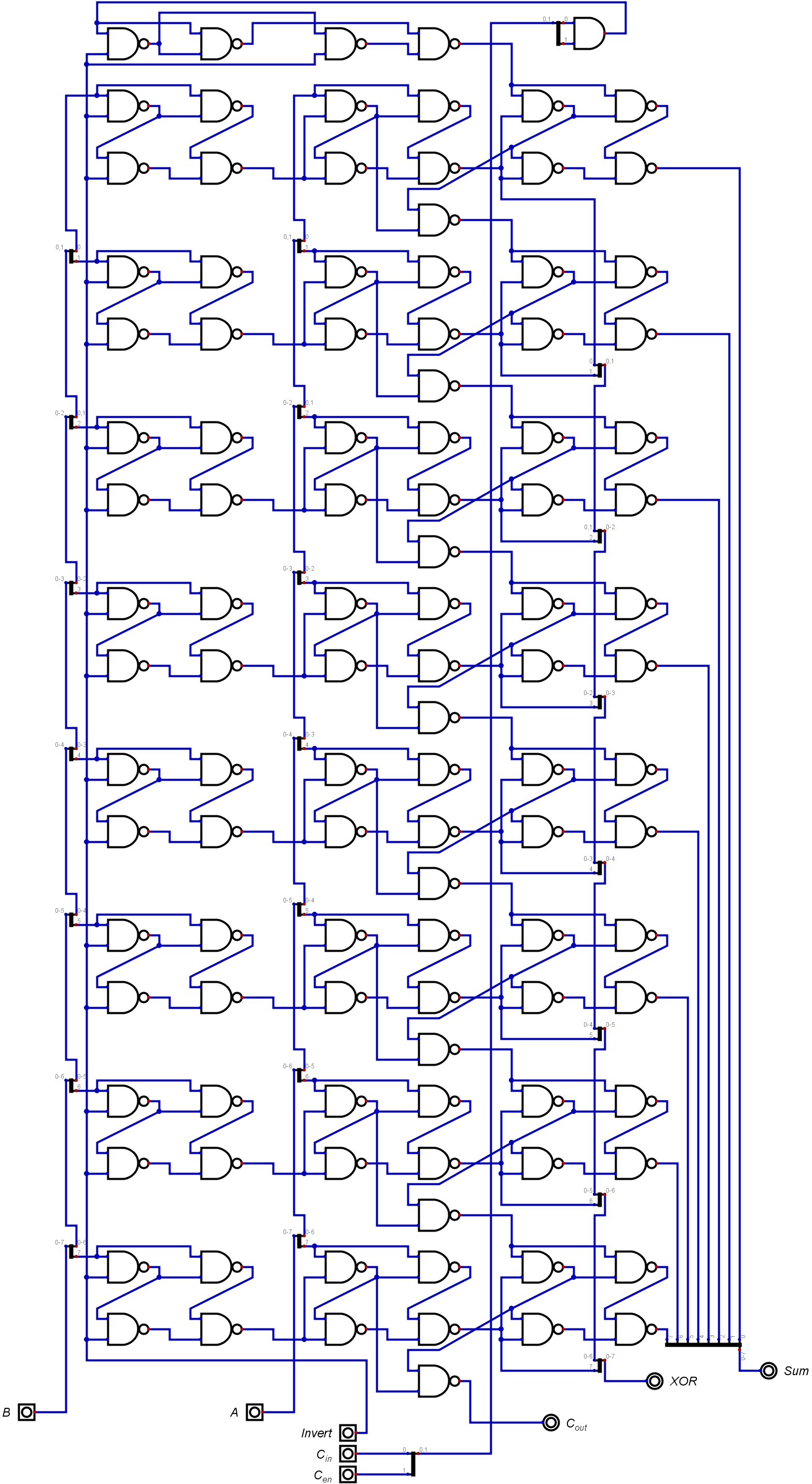
Here is an example of an XOR gate made of four NAND gates:
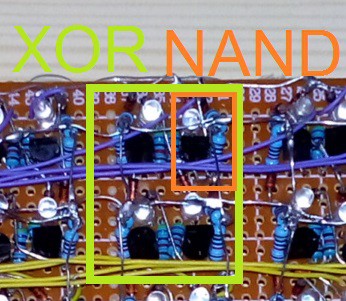
So, I am set to use these NAND gates wherever possible, with addition of AND gates where necessary. Using NOR / OR gates is not as parts/real estate efficient, and I am trying to avoid them.
 Pavel
Pavel
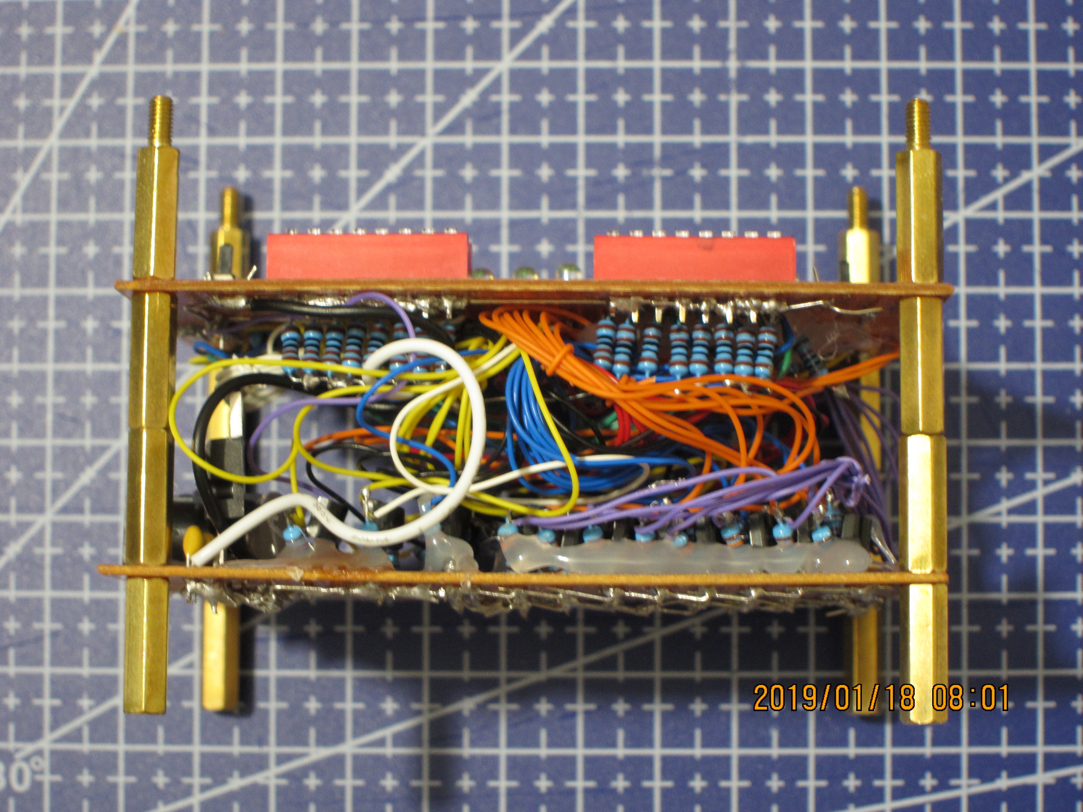
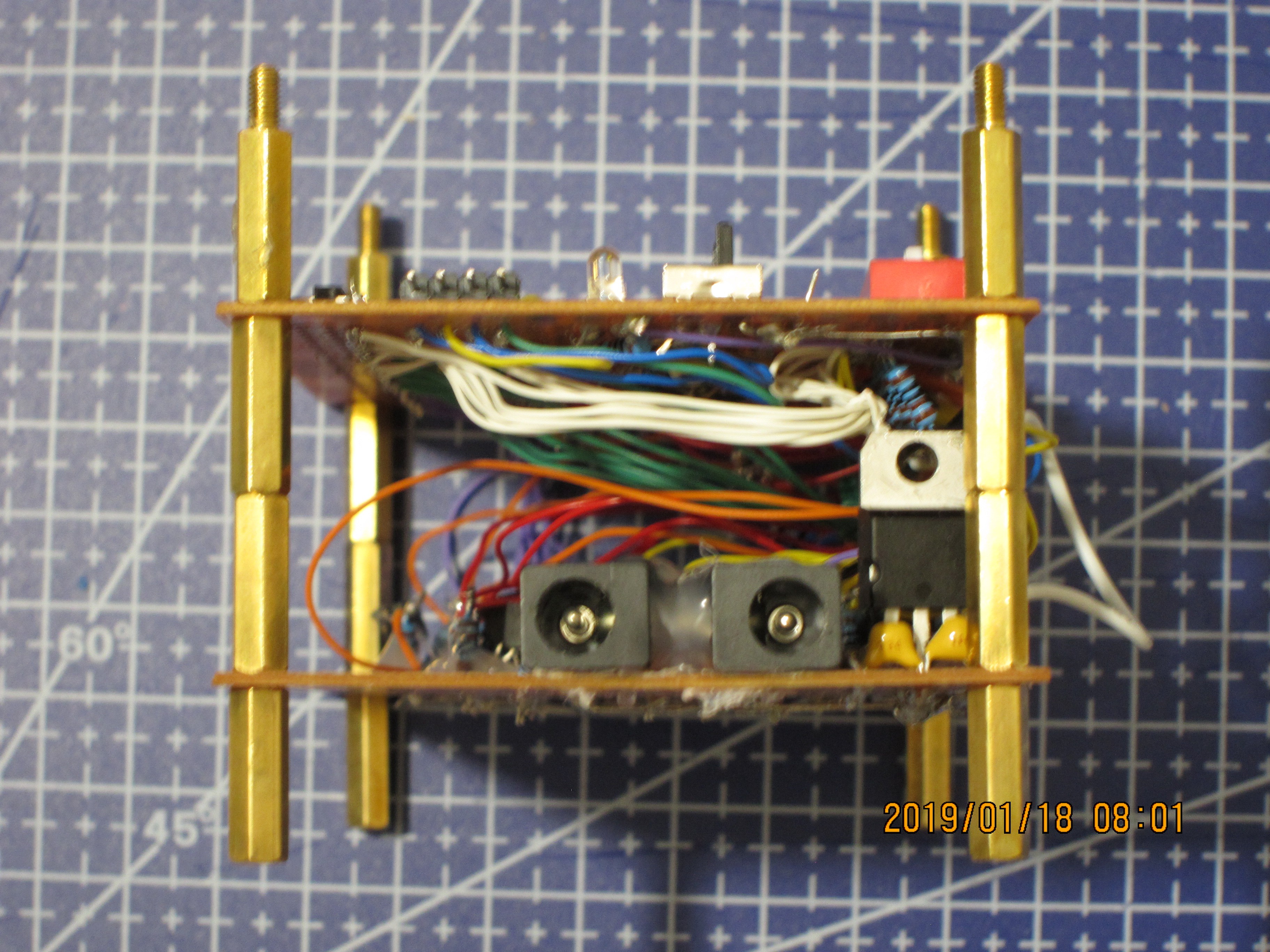
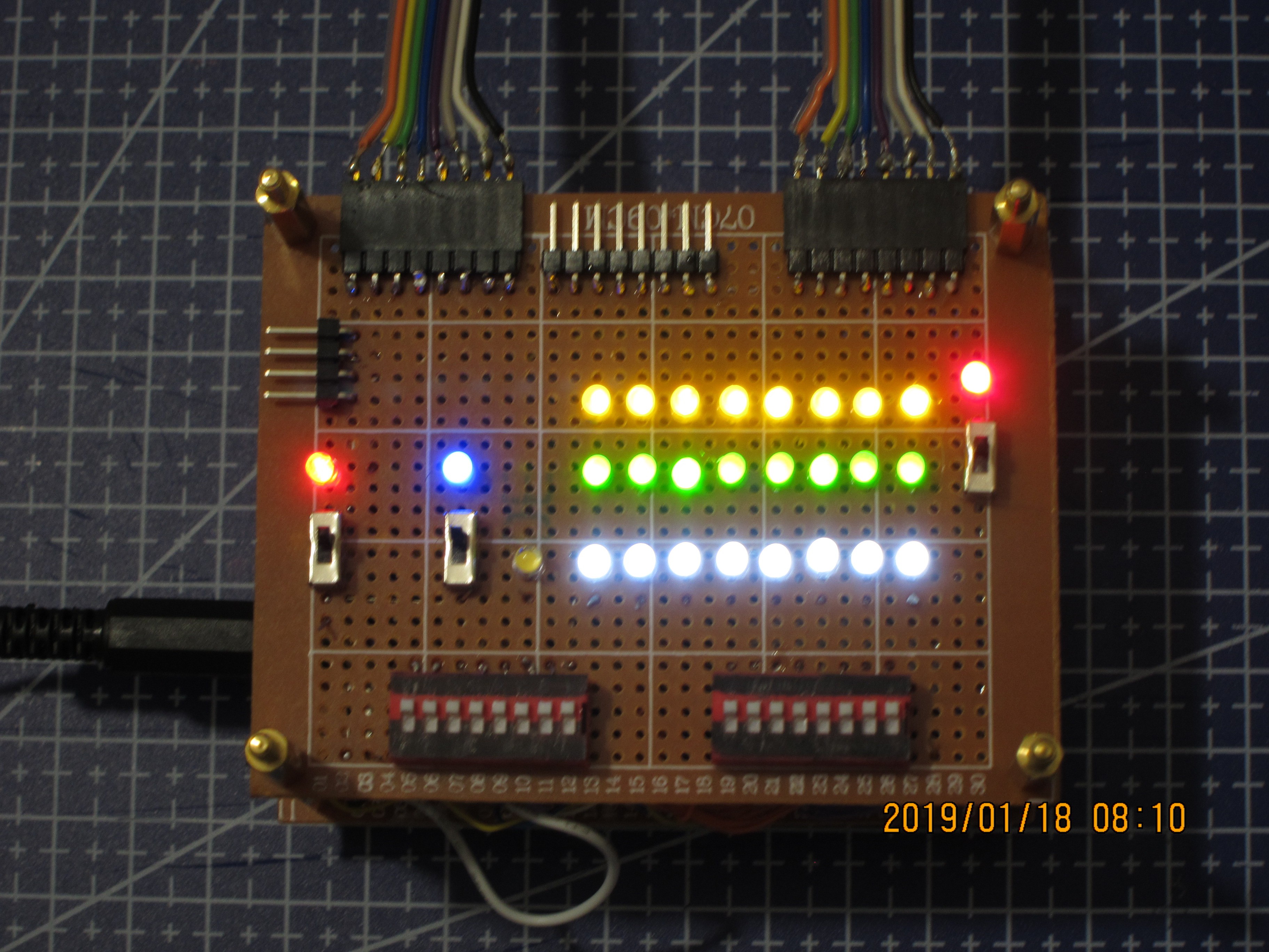
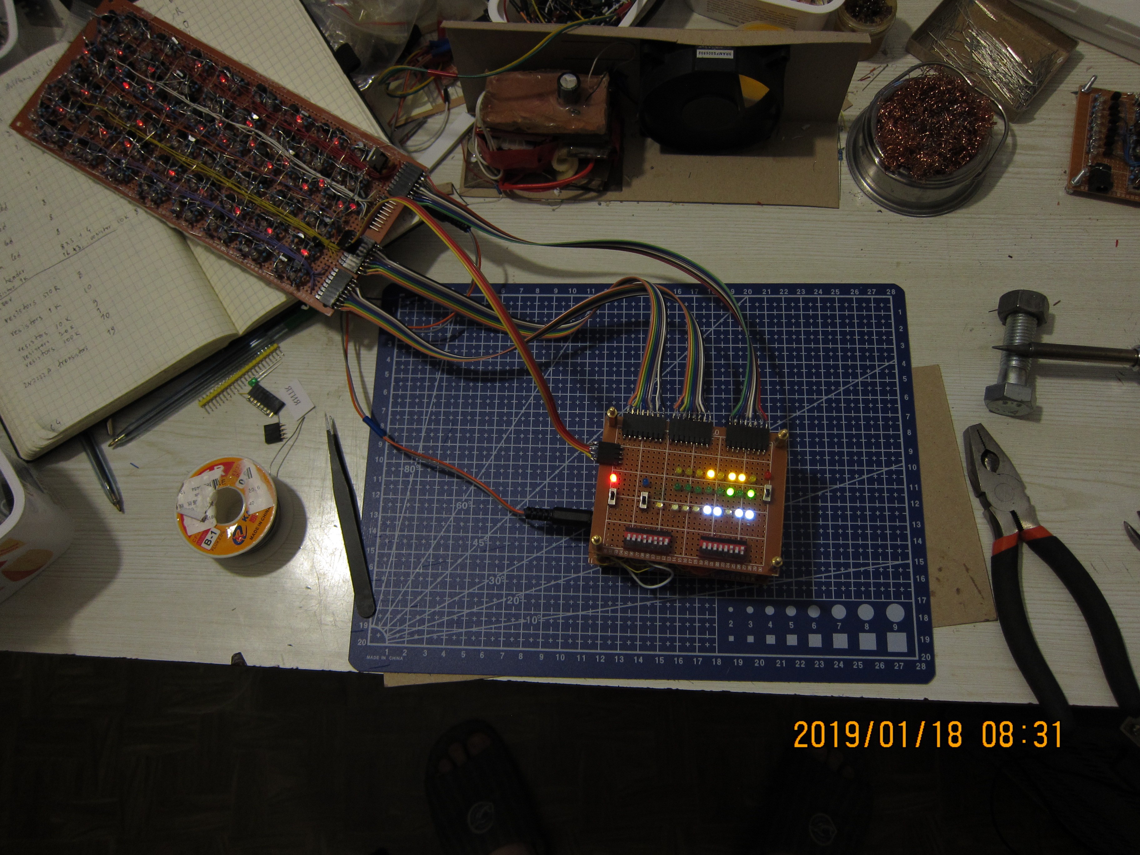
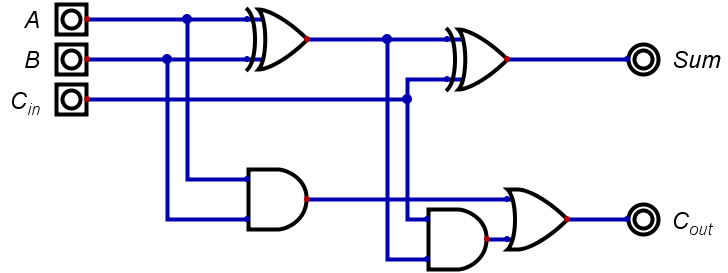
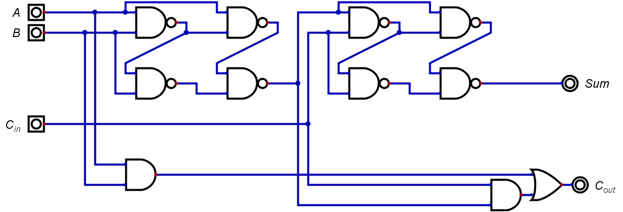
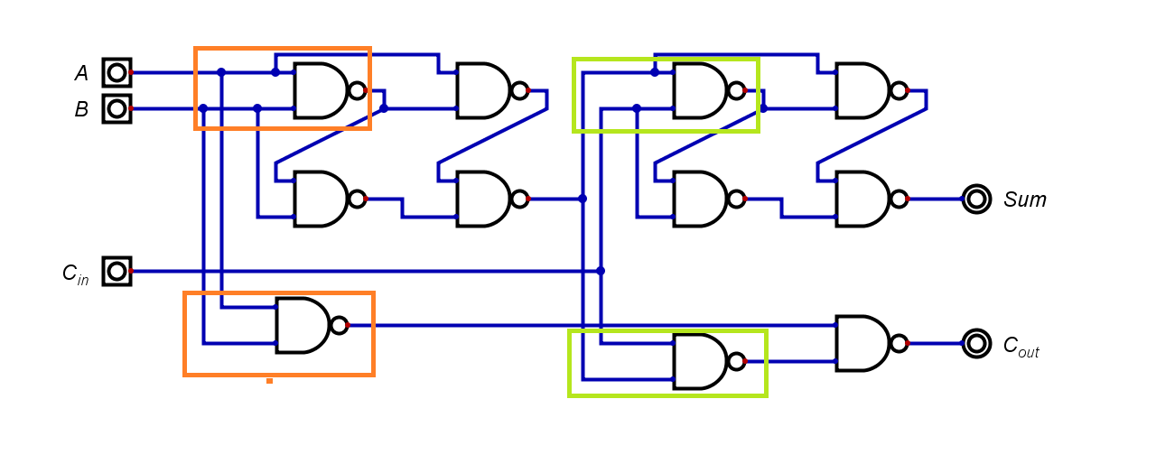

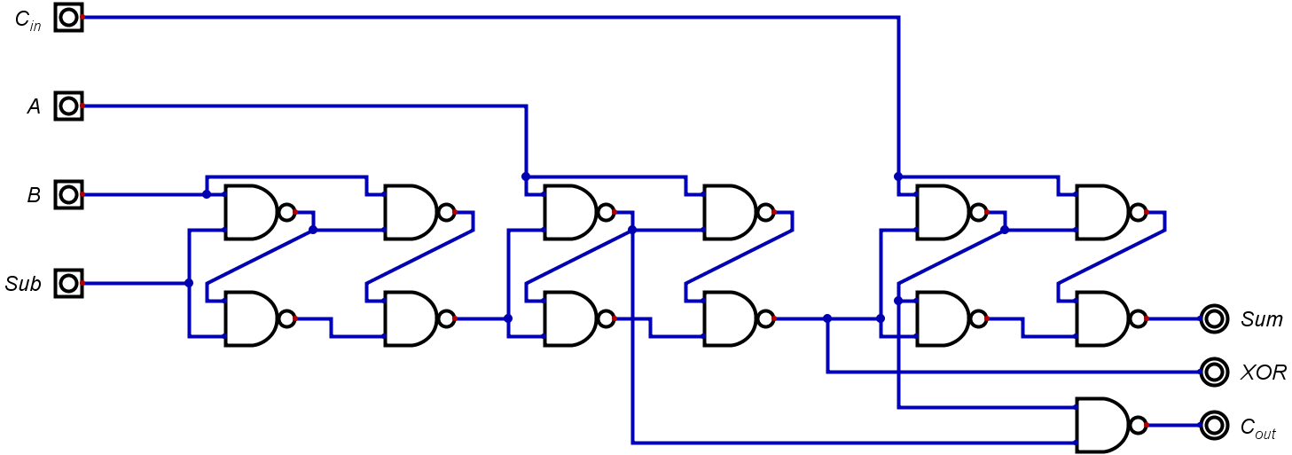


How would I make the ripple a higher or lower bit-rate? I thought you could remove half or add another for 8+ or 4- the unit.