-
Log #3: Firmware
02/20/2019 at 17:38 • 0 commentsThe firmware for this project is pretty straight forward, so I won't be cover it all, but I will discuss some of the code, and in a later log, I'll discuss what's left to implement and what I might re-implement in a later version.
Rolling average for analog inputs:
int temp_values[10];
int getTemp(int arr[]) {
 long temp_value = 0;
  for (int i = 0; i < 10; i++) { // loop through the array and sum values
    temp_value += arr[i];
  }

  for (int i = 9; i > 0; i--) { // move the values along
    arr[i] = arr[i-1];
  }

  arr[0] = analogRead(TEMP_SENS);
  temp_value /= 10; // average the adc inputs

  return tempCurve(temp_value, cal);
}
This function takes an input (from the temperature sensor amplifier) and returns an average of the last 10 readings (in C, through the function tempCurve. Note that the sensor is polled once per loop. This was done to smooth out the readings, without slowing down the loop with nested loops. But as you can see, there are still two loops, so it would probably be faster to simple poll the sensor 10 times and average it. This might be changed in a future version, but probably not, because as we will see later on, we have too much time on our hands already.
Converting to C:
int temp_multiplier = 91; // adjust slope of temp curve
const float adc_voltage = 0.0049; // 5V / 1023 = 0.0049 =  volts/adc-step
int tempCurve(int in, int offset) {
  float k = adc_voltage * temp_multiplier;
  // the linear expression for the temperature is: (adc_voltage*temp_multiplier*adc_in) + offset (offset is ambient + cal)
  // it is required that the output from the thermocouple amp is 1V/100C
  in = (k * in) + offset;
  return int(in);
}
This function takes the the raw value from the ADC and converts it to C. Ideally the temp_multiplier would be 100, since we were aiming for 1V/100C from the temp amplifier. Since we are a little of because of non-ideal component values, I've tweaked it to got a close match across the entire temperature range. This will be solved when the calibration function is implemented.
Waiting for temperature reading to settle:
if (current_time - sense_start < sense_time) {
      // sense
      //Serial.println("Sensing");
      if (current_time - sense_start > settle_time) {
        actual_temp = getTemp(temp_values);
      }
}
This is probably the trickest problem so far, and something I don't know the cause of yet. When the power is removed from the the heater, it takes a while for the sense voltage from the op-amp to settle back down, which means we have to wait before sampling the temperature of the iron. We could sense immediately, but that would cause problems in the next part of the code.
power_time = (set_temp - actual_temp) * 50;
power_time = min(power_time, 1000);
This calculation simply checks how far from the set point we are and sets the time for the iron to be on before shutting down again to measure the temperature. If we were to measure immediately, we would start at the measured temp being above the set temp, and keep measuring until the actual temperature was under the set temp, but since the temperature decreases over time, we would always end up powering on the iron the minimum time, because the measured temp is only a tiny bit below the set temp.
-
#Log 2: MOSFET bootstrapping
02/08/2019 at 12:58 • 1 commentAs discussed in the previous log, I wanted to build this project with components at hand. This, combined with issues in amplification meant I would have to use a N-channel MOSFET as a high-side switch. I knew that this wasn't the common application for N-channel MOSFETS, but I never understood why. Here is what I learned:
First, let's look at the problem. A MOSFET is controlled by the electric charge on its gate, in respect to the source. Basically, for a N-channel MOSFET, you need your gate to be at a higher potential than the source (a positive Vgs) for the transistor to turn on. In my case, the Vgs required to turn on the transistor is about 4.5V, that is; the gate needs to be 4.5V about the source.
This is the reason that N-channel MOSFETS are generally used as a low-side switch. Any (positive) voltage at the gate will be at higher potential than the source, because the source is connected to ground. This is not the case when in the high-side configuration. Let's take a look:
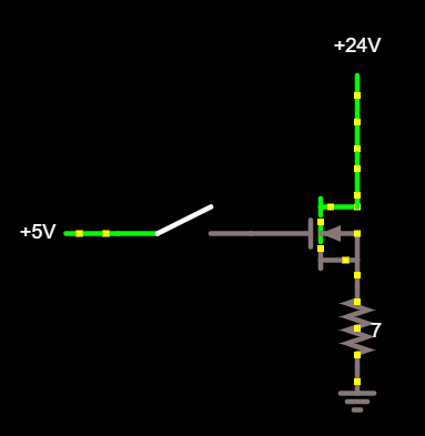
If you are like me, and have a limited intuition about these things, this configuration looks like it would work fine, When the switch is closed, the gate will be at 5V, and the source is at 0V, so what's the problem?
When the the switch is closed, the transistor does turn on, however, the voltage across the resistor cannot rise above Vgate - Vgs_threshhold (5V - 4.5V). This results in the load having 0.5V across it, and we get 0.5V / 7ohm = 71mA through our load. Far from enough to drive a soldering iron.
What if we use the supply rail to drive the MOSFET? Let's look at the following configuration:
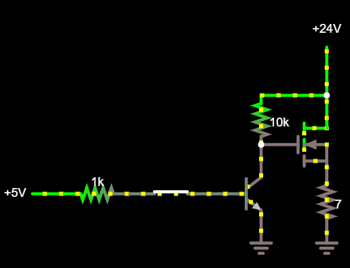
Here, we use a NPN BJT to drive the gate of the MOSFET. When the BJT is ON, the gate is pulled low, and the MOSFET is off. When the BJT is OFF, the gate is pulled to the supply rail through the 10k resistor.
Great! Now we have 24V at the gate, surely that solves the problem! But no, this makes our problem worse.
When the gate is pulled to 24V, the MOSFET turns on and passes current through to the load. But once again, the voltage across the load can't rise above Vgate - Vgs_threshhold (24V - 4.5V = 19.5V). This results in 2.8A through the load. Great, but wait! What about those 4.5V that are missing across the load? They don't magically disappear. Instead, they are dropped over the MOSFET. 4.5V * 2.8A is over 12W. That's way too much. Not only would the MOSFET heat up far to much, but we also lose 15% of our theoretical max power of 82W.
Here's what I did:
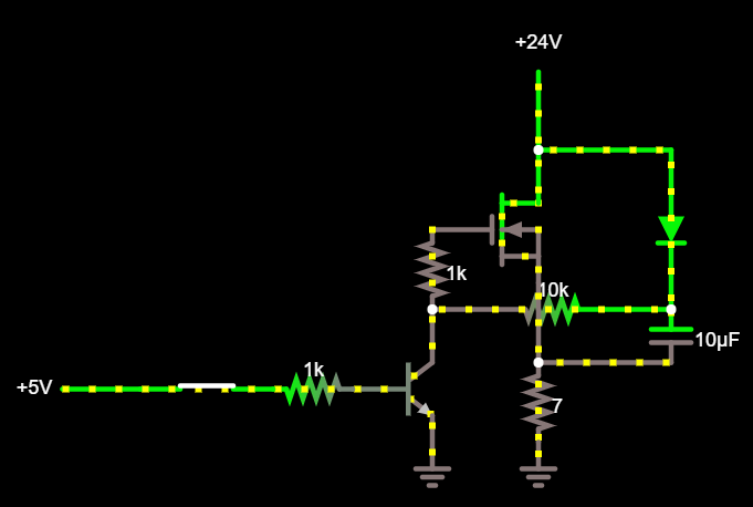
We can use the capacitor and diode on the left side of the diagram to "capture" the potential difference over the transistor when the transistor is off. The capacitor charges through the diode, until there is 24V across it (minus the forward voltage of the diode). The NPN BJT is initially on, which means the gate of the MOSFET is pulled low and will not conduct. When the BJT is turned of, the voltage across the capacitor is transferred to the gate of the MOSFET, turning it on. This is where the magic happens.
As the potential across the load rises, the potential at the negative side of the capacitor rises. The cap can not discharge (bar reverse leakage current of the diode and leakage current through the gate of the MOSFET), so it will maintain 24V volts across it. This means that if there is 24V across the load, we have 24V+24V (ideally) at the MOSFET gate! Perfect, now we have produced a Vgs of 24V, plenty to keep the MOSFET fully on. (Careful though, Vgs has an upper limit, and overloading it can damage your MOSFET).
I copied this solution straight from this video by Julian Ilett and this one by 0033mer.
In conclusion: There are pros and cons with using this configuration for high-side switching.
Pros:
- N-channel MOSFET's are more widely used, and one might be more likely to have one at hand.
- Lower on resistance, leading to higher efficiency and less heat.
- Easy to drive
Cons:
- Large number of components (all though they are all what I would consider jellybean parts)
- Not suitable for higher frequencies. (I haven't calculated or simulated this but it does need quite a large capacitance to work, and that is rarely great at higher frequencies).
- Potentially harmful to the MOSFET if the Vgs is too high.
-
Log #1: Thermocouple and amplification
01/31/2019 at 19:37 • 0 comments
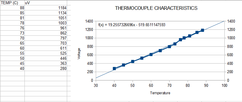
As outlined in this article/log by Marius Taciuc, the thermocouple in the HAKKO clone tips seem to be type C. I did some measurements of my own, by boiling a cup of water, sticking the iron in the cup, together with a cooking thermometer and plotting the thermoelectric voltage against the measured temperature.Even though my methods weren't as good as Marius', I came to the conclusion that I could expect about 19uV/C.
Since all I had at home was N-channel mosfets, I was planning on doing lowside switching and using a differential amplifier for amplifying the voltage of the thermocouple. How ever, I couldn't get this to work. My theory is that the the voltage was simply to small for the LM358 to accurately amplifiy. I tried my best to match the resistors for the differential amplifier, as well as using opamp followers for the outputs, but nothing seemed to help.
Instead I tried using a simple non-inverting amplifier. This would require a high side switch (more on this in a separate log) since it required common ground, but this way, the amplificatoin seemed to work without issue. The initial plan was to make sure that the amplified voltage was 1V/100C. As it turns out that requires some very precis resistor matching.
I settled for for 500k (1M // 1M) and 1k, for Rf and R1 respectively. for an approximate gain of 501, depending on the exact values of the resistors. This give me about 0.95V/100C. I can compensate for the discrepancy in software.
YATSS (Yet another T12 soldering station)
An arduino-based temperature controlled soldering station for the ubiquitous T12 clones.


