Address decoding for the m68k is a bit more involved than for most (all?) of the 8-bit CPUs that were around at the same time, and so requires a bit more careful design. The specific things that make it complicated are:
- The larger (16MB) address space
- The different address spaces supported by the processor (e.g. Supervisor program)
- The /UDS and /LDS lines (used to select upper byte, lower byte, or both bytes for a 16-bit operation)
- The fact that there's no separate IO address space
- The requirement to have ROM at 0x00 for the first four clock cycles, then RAM there afterward
My address decoder design completely ignores the second item on that list, and just uses one address space. I may decide later to expand to support the different address spaces, but for now I don't need it.
The /UDS and /LDS lines are easily supported in the usual way for m68k builds - having odd and even ROM and RAM chips. This means that chips must always come in pairs, but it simplifies the logic quite a lot and anyway, I've found parallel chips are easier to get with 8-bit data width.
The last point is quite interesting - At startup, the m68k family expects the first eight bytes of memory to contain two 32-bit longwords, one each for the initial stack pointer and the initial program counter. Therefore, at startup (or on reset) the first eight bytes of memory should really be ROM. However, during normal execution the m68k requires RAM at the bottom of memory, to allow interrupt vectors to be modified (at least, the 68000 does. With the 68010 its not strictly necessary due to the 010 having the VBR register, but I want to have RAM at the bottom of memory in normal running anyway). The 68000 Programmers Manual does actually recommend a solution to this - simply map ROM low for the first four clock cycles. So the address decoder has to have a way to make that happen.
The memory map I decided I wanted for this system is:
- 0x000000 - 0x0FFFFF - Onboard RAM (1MB)
- 0x100000 - 0xF7FFFF - Expansion Ram (Initially, will just generate /BERR)
- 0xF80000 - 0xFBFFFF - IO (256KB)
- 0xFC0000 - 0xFFFFFF - ROM (256KB)
(With the caveat previously mentioned that, for the first four cycles after reset, ROM will be mapped low).
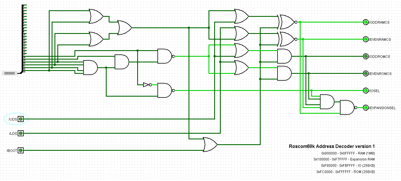
I fired up Logisim, and after a few (read: a lot of) iterations I had the following design, which I think does everything I need it to do:

The address bus is at the top left, and currently set to address 0x0. Notice the /BOOT line, which is low in the image - this is how I'm controlling whether the ROM is currently mapped low or not. You can see that, with that active, the /ROMCS lines are active.
When the /BOOT line is high (i.e. during normal running) the /RAMCS lines are active instead:

As you can see, the /BOOT line just directly selects ROM, bypassing the normal way it is selected, using the highest four address lines. This means that ROM is just shadowed low with this setup.
It also doesn't do anything with the /UDS and /LDS lines, meaning that when /BOOT is low, the chip can only do full 16-bit memory accesses - this should be fine because, according to the manual, that's all it will do during those first clock cycles, in order to read those two 32-bit values. After that point, /BOOT will go high, and the /UDS and /LDS lines are decoded as normal and used to select the appropriate chips.
The /IOSEL line indicates that the address decoded falls into the IO range - this will need further decoding to select the appropriate IO device - since I have none at this point, I'm doing nothing further with it. The same goes for the /EXPANSIONSEL line (which indicates a RAM address outside the 1MB I'll have on the board) - I might eventually use this to drive decoding on a memory expansion board, but for now I'll just tie it to /BERR on the CPU.
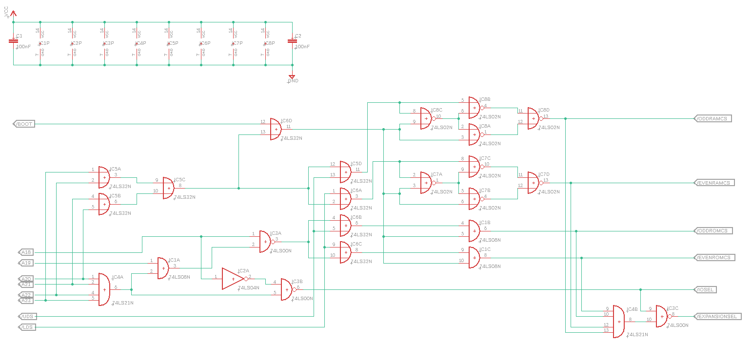
This is how it looks in EAGLE:

The major difference to notice is that I just haven't been able to get hold of XNOR gates in the 74LS series. There are some listed but they seem only to be available in the later HC series which isn't TTL compatible. I could probably have gotten them in HCT, but to be honest I have a bunch of 72LS02 chips so I decided to just go ahead and build the XNORs with NOR gates. It ups the chip count by one, but to be honest I was tired of trying to source the chips and wanted to just go with what I had.
That said, this still isn't built yet because I'm waiting on a couple of chips (a 74LS32 and a 74LS00) but they should be here in a few days, so I'll update once its built.
The one thing left to do is handle that /BOOT line, which I'll write up in the next log.
 Ross Bamford
Discussions
Become a Hackaday.io Member
Create an account to leave a comment. Already have an account? Log In.
Nice work. If you are not wedded to the idea of using TTL parts throughout, consider replacing all of that with a GAL like the 16v8. They are only a couple of dollars and easily do the job of ten or twenty gates. For the software there are free apps like galasm. You do need a programmer though.
Here's a log from my current project about GALs: https://hackaday.io/project/164087/log/160589-programmng-the-gal
Incidentally watching your project with interest as I have a bunch of 68k CPUs in the retro parts box.
Are you sure? yes | no
Thanks, Ken!
I'm not especially wedded to using TTL parts throughout, and I did read up on GALs a bit recently (coincidentally after reading the log you linked above :) ), but I figured for my learning I'd be best to start with baby-steps and do this with basic logic, and then look at more advanced stuff like programming a GAL. It's definitely something that's on my radar for the future though (Probably somewhere around the time I'm trying to wire all this up!)
You have some really cool projects, so I'll definitely look forward to your 68k build :)
Are you sure? yes | no