-
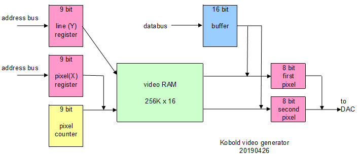
Plan for video generation
04/26/2019 at 19:05 • 0 comments[ Edit: around one year later, a new VGA generation project has started, with better specs ! ]
Trying to have the hardware simple, and keeping in mind that 'large' SRAMs are easy to obtain, the choice was made to have just a single basic video mode.
That is, 640 x 480 pixels, with 256 colors per pixel. The pixel time for VGA is 40nSec.
The hardware needs assistance from software in order to operate correctly.
![]()
The pixel counter will increment every 80nS, so the video RAM will deliver two new pixel values every 80nS. The 8 bit color values go to the 'first pixel' and 'second pixel' registers. During the next 80nS, each of the outputs of these registers will be enabled for 40 nS.
When the pixel counter has reached a certain value, an interrupt will be given to the CPU. In the interrupt, the CPU will:
- obtain exact synchronization with the pixel counter
- when the pixel counter is exact 199, reset the pixel counter to zero, to obtain 32 uSec line duration
- start the horizontal sync signal
- obtain access to the video RAM, disabling the pixel counter and the updating of the two pixel color registers, and enabling the pixel(X) register. It can now, after setting the correct pixel address in the line and pixel registers, write new data to the video RAM. The line and pixel registers may be latches, so the data can be written in the same cycle together with the address. Several locations may be written, depending on the available time during blanking.
- set the line (Y) register to the starting point of data for the next line
- when the end of a frame has been reached, do functions for frame synchronisation
- stop the access to video RAM, and stop the horizontal sync signal
- end the interrupt
The sequence of actions might be a little bit different than listed here.
The actions might be done by microcode, and the 16 bit processor can deliver 16 bit at a time, so this will be fast enough for most operations. If there are applications (games) that need higher speed, resolution could be dropped to 320 x 240 (TBD to be determined). [ edit: Sprites were added to the video system, see here]
Since the starting point of a line is under software control, it will be easy to do fast vertical scrolling. A clear screen will also go fast, because only a single cleared line has to be present, and all other lines can point to the same cleared line.
-
System diagram
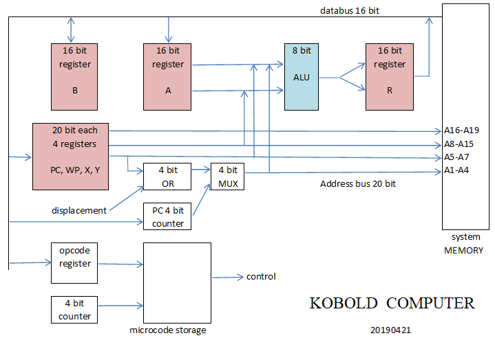
04/21/2019 at 09:13 • 0 comments![]()
This is the new system diagram for the 16 bit bus system.
The program counter is in the set of four registers. However, incrementing the program counter would either cost several extra cycles or extra hardware. In this low-part-count solution, the lowest 4 bits of the PC are in a hardware counter, and the other bits are provided by the register set. When the 4-bit counter overflows, the microcode will add 16 to the part that is in the register set.
Register B is a temporary register for MOV instructions. It is loaded with 16 bit data from a source memory location, and then its contents can be stored to a destination memory location. These locations include the R0-R7 because they are also in memory. Register B can also shift data. It is constructed of two 74HC299 devices.
The ALU can do only two instructions, ADD and a logical instruction, NOR or NAND, [TBD, to be determined]. Other instructions are done by microcode. The ALU takes one operand from one of the registers PC, WP, X or Y, and the other operand from A. The outputs of these registers can be tri-stated in 8-bit sections, so adding A to X will first enable the low section of X and A, add them and put the result in the low section of R. Then the same will be done for the high byte.
Note that the ALU can also swap the two bytes in a word. This will be used when byte instructions need to store a byte in the upper 8 bits of a memory word. The microcode will look at address bit 0 to determine if a byte must be moved to or from the low or high part of a memory word. For storing a byte to a memory location, the microcode can disable writing to one of the two bytes that are in a memory word, so when a byte is written, the other byte in that memory word is not affected.
-
Design upgrade
04/18/2019 at 11:27 • 1 commentThe current design of the microcode structure is almost complete, with just a few loose ends that have to be solved.
However, the total design effort for the project will be quite huge, and it would be a pity if the result is inferior on certain aspects. It seems that with a little more effort, a better result can be obtained (at the cost of a few more components).
This will focus on two main aspects:
- Most instructions are just moving data around. If we change the bus from 8 to 16 bit, the system will run almost twice as fast. The ALU might
stay 8 bit to keep the part count reasonable (This will perhaps only cost a single extra cycle for instructions that do calculations). - Several aspects of the Kobold are inspired on the PDP11. With some more effort, the design could be such that the microcode can implement a binary
compatible PDP-11 instruction set. (This will only be practical with a 16 bit bus).
So, work to do !
- Most instructions are just moving data around. If we change the bus from 8 to 16 bit, the system will run almost twice as fast. The ALU might
-
Opcode handling
04/15/2019 at 17:17 • 3 commentsThe Kobold is advertised to handle 16 bit instructions, but everything is 8 bit. Even the microcode is only 8 bit wide. How does it work ?
[ What you need to know for the examples: The program counter is in register R7 (as on the PDP11), and is copied into address register PC when needed. The lowest bit of the PC is always 0.]
EXAMPLE: 16-bit ADD
As example, take an instruction that adds (X+6) to register R4:
add (X+6),R4
The instruction is split into two parts, that operate almost independent of each other:
The first byte of the instruction is fetched from (PC) into the micro-program counter. From here, the micro-instructions determine the operation:
- First part:
- load the LSB of the 16bit accumulator with (X+6), (the LSB part)
- load the MSB of the 16bit accumulator with (X+6), (the MSB part)
- fetch an instruction byte from (PC+1) into the micro-program counter (changing flow of the microcode).
This instruction byte tells to add R4 (16 bits) to the accumulator and store the result back to R4:
- Second part:
- add the LSB of (WP+4) to the LSB of the accumulator
- add the MSB of (WP+4) to the MSB of the accumulator
- store the LSB of the accumulator back into (WP+4) (the LSB part of R4)
- store the MSB of the accumulator back into (WP+4) (the MSB part of R4)
The next section of the microcode will increment the PC and start the next instruction:
- connect the LSB of the PC (from the address registers) to the B-input of the adder of the ALU. The value 2 will be provided to the A-input of the ALU, so the byte value P+2 will be put in the accumulator.
- fetch the MSB of the pc from R7 [in the workspace] and put it into the accumulator, to make 16 bits complete.
- move the 16-bit accumulator contents to the pc in the address register set.
- fetch the next instruction from (PC) into the micro-program counter.
( from here, the micro-instructions for the next instruction are executed )
EXAMPLE: 8 bit immediate load
There are also instructions that have a single opcode byte, followed by an 8-bit immediate operand or z-page location. Branch instructions are an example of this.
As example, load register R3 with value 0x80:
mov #0x80,R3
- load the LSB of the accumulator from (PC+1)
- load the MSB of the accumulator with zero
- store the LSB of the accumulator in (WP+3) (the LSB part of R3)
- store the MSB of the accumulator in (WP+3) (the MSB part of R3)
Finally, the pc is incremented and the next instruction is fetched, as in the previous example.
-
Address registers schematic
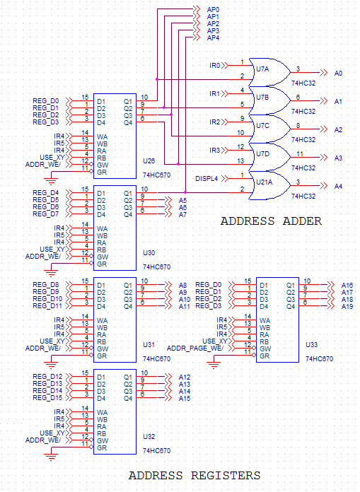
04/14/2019 at 18:17 • 0 comments![]() Here you see the schematic of the four address registers, with the five 74HC670 chips.
Here you see the schematic of the four address registers, with the five 74HC670 chips. Each address register holds 20 address bits. The four address registers are called PC, WP, X and Y.
Loading the address register
The inputs (REG0-REG15) come from the accumulator. The address register to write to is selected with the WA and WB inputs (that connect to bit IR4 and IR5 of the microcode byte). When ADDR_WE is active (low) the data is written into the selected address register.
The upper four bits (16-19) of the address register are written when ADDR_PAGE_WE is active.
Output of the address registers
The five 670's always put an address on the address bus (A0-A19), because the GR signal is always active [edit: in a newer version, the outputs can be tri-stated]. When the USE_XY signal is low, the PC or WP is connected to the bus (selected with bit IR4 from the microcode). When USE_XY is high, the X or Y register is connected to the bus, also selected with IR4.
Adding the displacement
At the upper right you see five OR-gates that "add" a displacement to the address. The lower four bits of the displacement come from the microcode byte. The fifth bit (DISPL4) comes from the control section. Since the displacement is not really added, it only works if the address in the address register is properly aligned. Alhough a four bit adder chip could have been used for the A1-A4, this only moves the problem when that adder has a carry. But having more than one adder chip here is against the minimum parts philosophy of the project.
The upper signals AP0-AP4, together with A5-A8 can be connected to the adder in the ALU. This connection is used for incrementing the PC. Only the lower byte of the PC is incremented. To cross a 256-byte boundary, an explicit instruction will be needed.
-
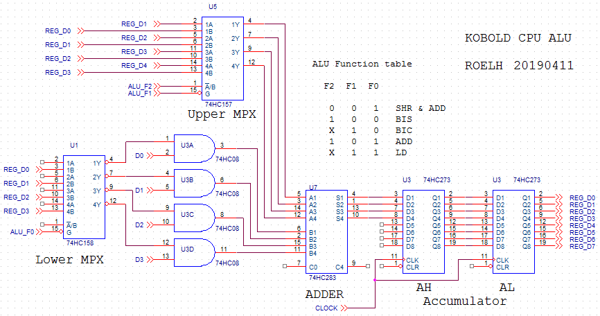
The ALU of the Kobold
04/12/2019 at 20:01 • 0 commentsThis is the current state of the ALU design. There are still several loose ends. Carry signals for addition and shifting are not yet present. The ALU is 8 bits wide, but for clarity I only show 4 bits. (Clicking it will show a better readable version).
![]()
The ALU functions are LOAD, ADD, BIS, BIC, SHR and SHL
The ALU is intended to work on 16 bit words, in two sequential cycles that each handle a byte.
ADD function
The ADD function is the easiest to explain. The upper MPX (multiplexer) connects the output of the AL accumulator byte to the upper inputs of the adder chip, 74HC283. The lower MPX is disabled (by ALU_F0 signal), so all its outputs are high. That means that the input from the databus (D0-D7) is flowing through the AND-gates to the lower inputs of the adder chip. So, the adder will add the databus byte to the AL byte and deliver the result in AH.
Ooops... what is that lower byte doing in the high part of the accumulator ? And the accumulator has been clocked, so the high byte of the accumulator is now in the low byte ?
After the next cycle, it will be all right. The high byte coming from the databus will be added to the high byte of the accumulator, that is in AL now. The result will go to the AH register, and the previous result of the low byte will at the same time go to the AL register.
LOAD function
How do we put something in the accumulator ? We set the ALU-F1 signal (connected to the upper MPX) to 1. This disables the upper MPX, its output will be zero. We now do the ADD operation. The databus contents will be added to zero, and the result will be put in the accumulator.
BIC function
For the BIC (bit clear) function (that is a logical AND where one of the operands is inverted), the upper MPX is disabled but the lower MPX is now enabled. The lower MPX inverts the data (it is a 74HC158). The following AND gates will give result: DATA and (not ACCU). The adder will add zero to this, so that does not change the result. So the result is that any bit that was set in the accumulator, will cause the same bit from the databus input to be cleared.
BIS function
The BIS (bit set) function (PDP11 parlance for logical OR) is similar to BIC, but now also the upper MPX is enabled again. so both adder inputs can receive data. When an accumulator bit is 0, the AND gates will transfer the databus inputs, the adder will add the 0 bit to it, so result for this bit is 1 (if there was no carry from previous bit). And when an accumulator bit is 1, it is inverted by the lower MPX so it delivers 0 to its AND gate, so the lower input of the adder will be 0. The adder output will be 1 because the upper input is 1 and the lower input is 0. The key idea is, that at the adder, the two inputs for a certain bit are never both 1. In this case, the adder will never generate an (internal or external) carry, and will behave as four OR gates.
SHR function
Finally, the SHR (shift right) function can be done by the upper MPX, because it has a shifted version of the accumulator bits connected to one of its input groups. The databus input should be zero (or not, in that case it will be added to the result).
SHL function
SHL (shift left) is the same as adding.
Other functions
A few functions are missing, but they can be composed from the functions that are available. This can be done in microcode, so the instruction set can still contain these missing functions. It will only have a small impact on performance. The functions that I'm talking about are SUB, XOR and NOT.
[edit: ALU design changed due to switching to 16 bit design, new version is here]
-
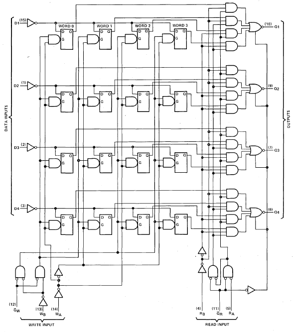
Address generation
04/10/2019 at 14:15 • 0 commentsFor generating the memory address, the square inch processor had only a H-L register pair, that had to be reloaded each time when another address was needed. For the new processor, I want to have several addresses on standby, ready to be connected to the address bus when needed. I also want 20 bit addresses.
The 74HC670 seems to be very suitable for this. It has 4 latches of 4 bits each (and only 16 pins). If we use five of them, we have four 20-bit registers. 1-to-4 decoders for read and write are built-in ! Here are the internals:
![]()
Bits 1 to 4 will get or-gates or an adder to add the 4-bit word-displacement to the address. The lowest address bit, bit 0, is used to select upper or lower byte in a word.
So, the address generation takes only 6 chips !
-
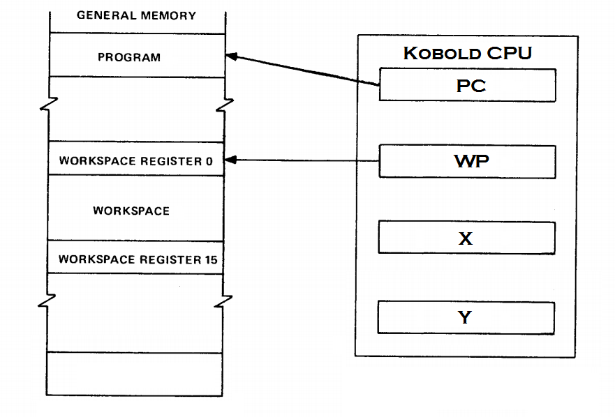
High level instructions
04/09/2019 at 19:45 • 0 commentsFor the instructions, there will be the following registers visible:
Hardware address registers: (20 bit wide)
PC program counter
WP workspace pointer
X index register
Y index registerRegisters in RAM (16 bit wide): R0 - R15
The WP register points to the location of R0.
![]()
The instructions will follow the assembly format of the PDP11 computer.
Most instructions will have two operands, like:
MOVB #17,R4 ; load register R4 with the value 17 (decimal)
Instructions handle a single byte or a word (2 bytes).
Possible instructions are:
MOVB src,dst  ; move data (byte size)
ADDB src,dst  ; add data (byte size)
SUBB src,dst  ; subtract data (byte size)
BISB src,dst  ; bit set  (byte size)
BICB src,dst  ; bit clear (byte size)
BITB src,dst  ; bit test (byte size)
CMPB src,dst  ; compare (byte size)

MOV src,dst  ; move data (word size)
ADD src,dst  ; add data (word size)
SUB src,dst  ; subtract data (word size)
BIS src,dst  ; bit set  (word size)
BIC src,dst  ; bit clear (word size)
BIT src,dst  ; bit test (word size)
CMP src,dst  ; compare (word size)

BR label     ; branch. conditional versions also available
JSR label    ; jump to subroutine
RTS          ; return from subroutine
There will be more instructions, but these are the main ones.
Now the addressing modes:
Rn        ; general register
X, Y, WP  ; address register
(Rn)      ; register indirect
(Rn+)     ; register indirect with post-increment
disp(X)   ; indirect with displacement, displacement 0-15 words
disp(Y)   ; indirect with displacement, displacement 0-15 words
#number   ; immediate data
label     ; zero-page memory location
Most instructions will be 2 bytes (16 bits).
There will be special instructions to load the four upper bits of X, Y and WP. This might be done with instructions that handle LONG operands (4 bytes).
Due to the limited number of opcodes available, not all combinations of addressing modes will be available in the final instruction set.
It is under investigation to make the instruction encoding equal to the encoding of the PDP11.
Well all that has to be done is write microcode to implement this.... Oh wait, there is no hardware yet....
[edit: new instructuction set is here]
-
Hardware registers and microcode
04/09/2019 at 18:59 • 0 commentsREGISTERS
The data width of the CPU is 8 bits.
The CPU will now have four address registers (instead of the single HL register pair ).
The address registers are 20 bits wide. Regular instructions will operate on the lowest 16 bits, and there will be special instructions to fill the upper 4 bits of each register.
Register naming:
PC program counter
WP workspace pointer
X index register
Y index registerThere will be two 8-bit accumulator registers, coupled to the new ALU. They can, together,
contain a 16 bit value.MICROCODE
Hopefully, the microcode can stay 8 bits wide.
For the moment, this is the idea for the micro-instructions:
00AA DDDD  load accumulator 8bit, addr register AA with displ. DDDD
01AA DDDD  store accumulator 8bit, addr register AA with displ. DDDD
10AA DDDD  add to accumulator, addr register AA with displ. DDDD

1100 FFFF  set ALU function FFFF (instead of the default ADD)

1101 AA00  16-bit accumulator to addr. register AA (bits 0-15)
1101 AA01  16-bit accumulator to addr. register AA (bits 16-19)
1101 AA10  16-bit accumulator to addr. register AA if true (bits 0-15)
1101 AA11  16-bit accumulator to addr. register AA if false (bits 0-15)

1110 FFFF  reserved for I/O

1111 FFFF  microcode jump
[edit: a new version of the microcode is found here]
Kobold - retro TTL computer
A 16 bit computer with 20 address bits and video display, from just a few TTL and memory chips. Instructions resemble 68000 / PDP-11.
 Here you see the schematic of the four address registers, with the five