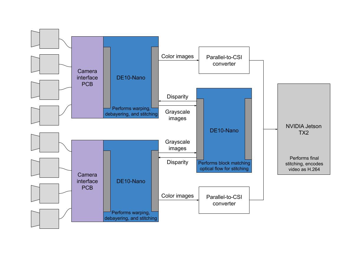
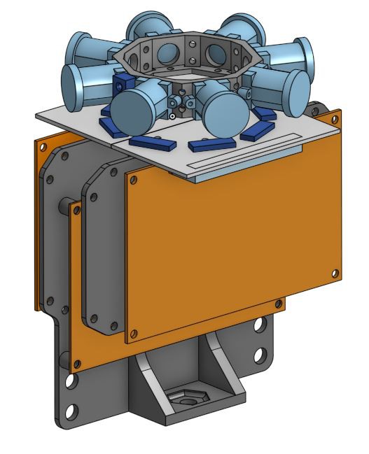
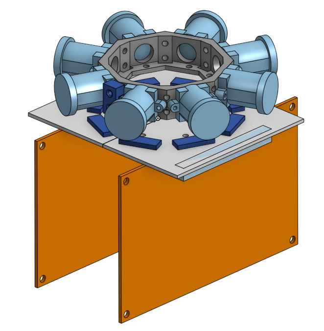
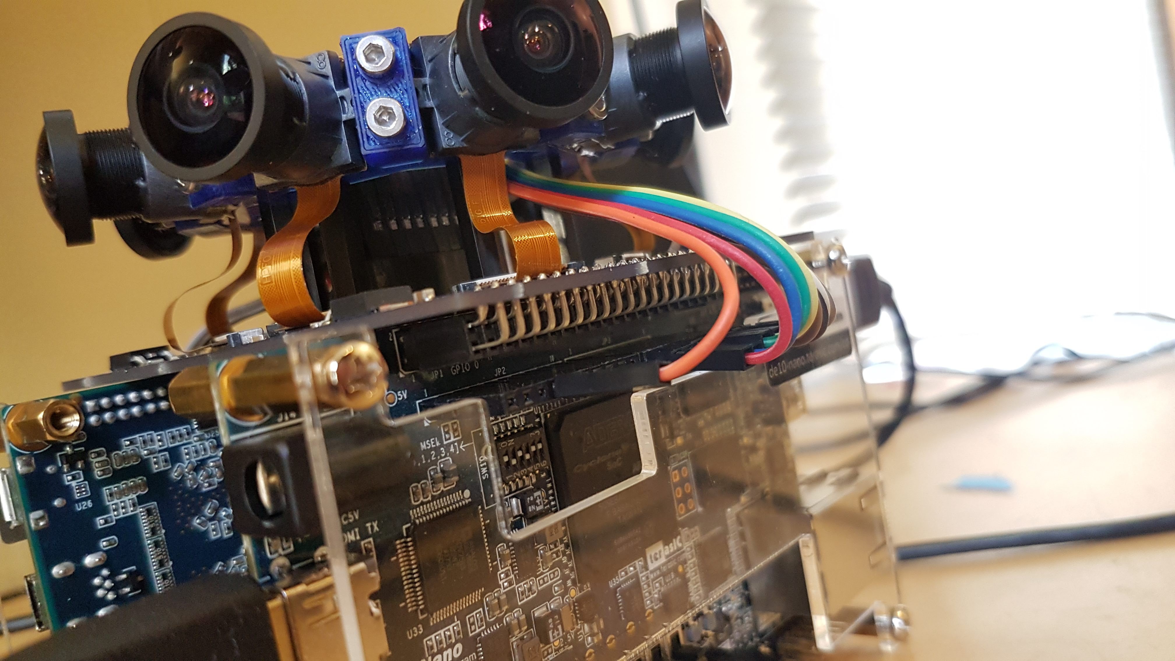
Shown below is the high-level data flow and hardware connection diagram for the camera.
Here are the components of the project that I have successfully implemented so far:
- Camera I2C control
- Debayering module
- Camera image warping modules
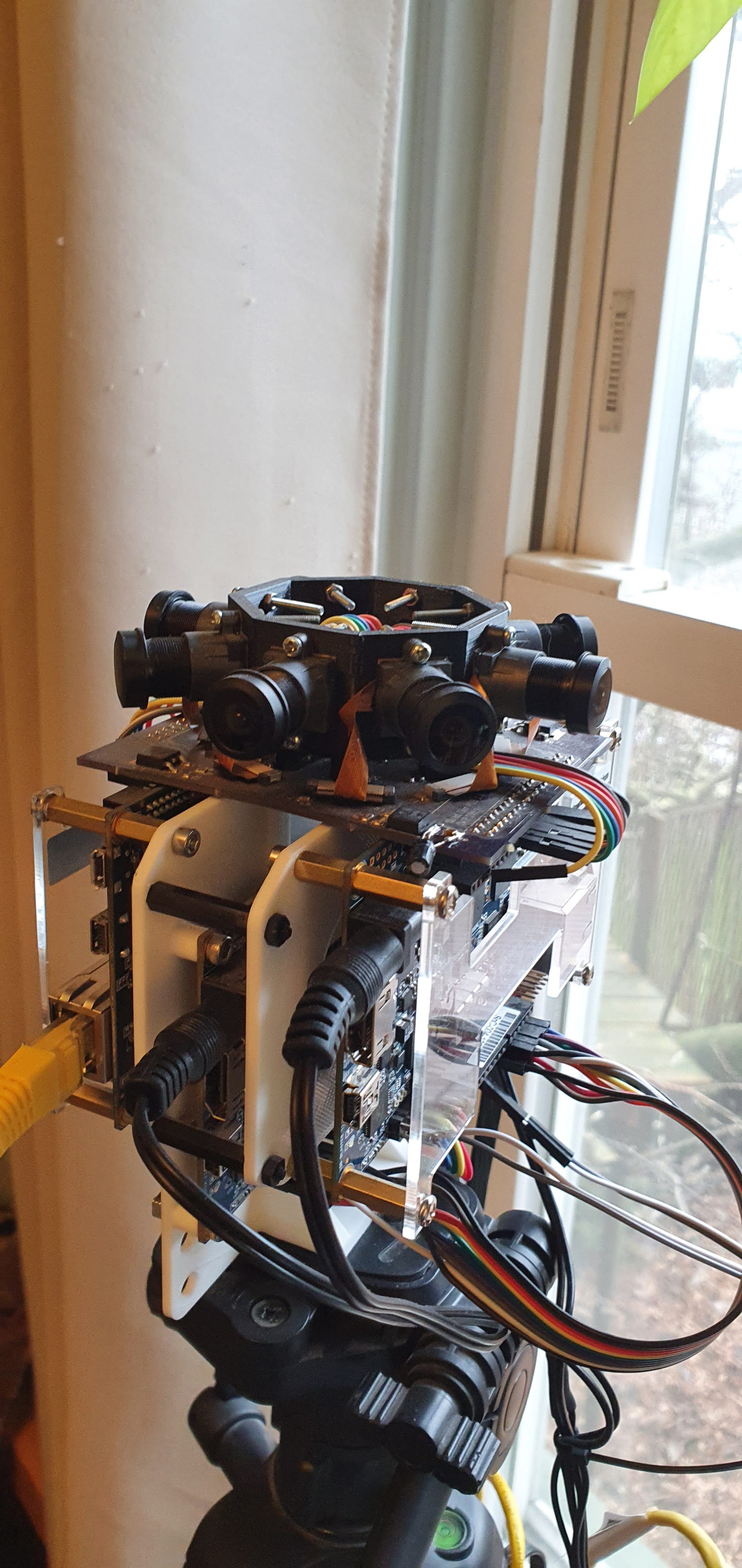
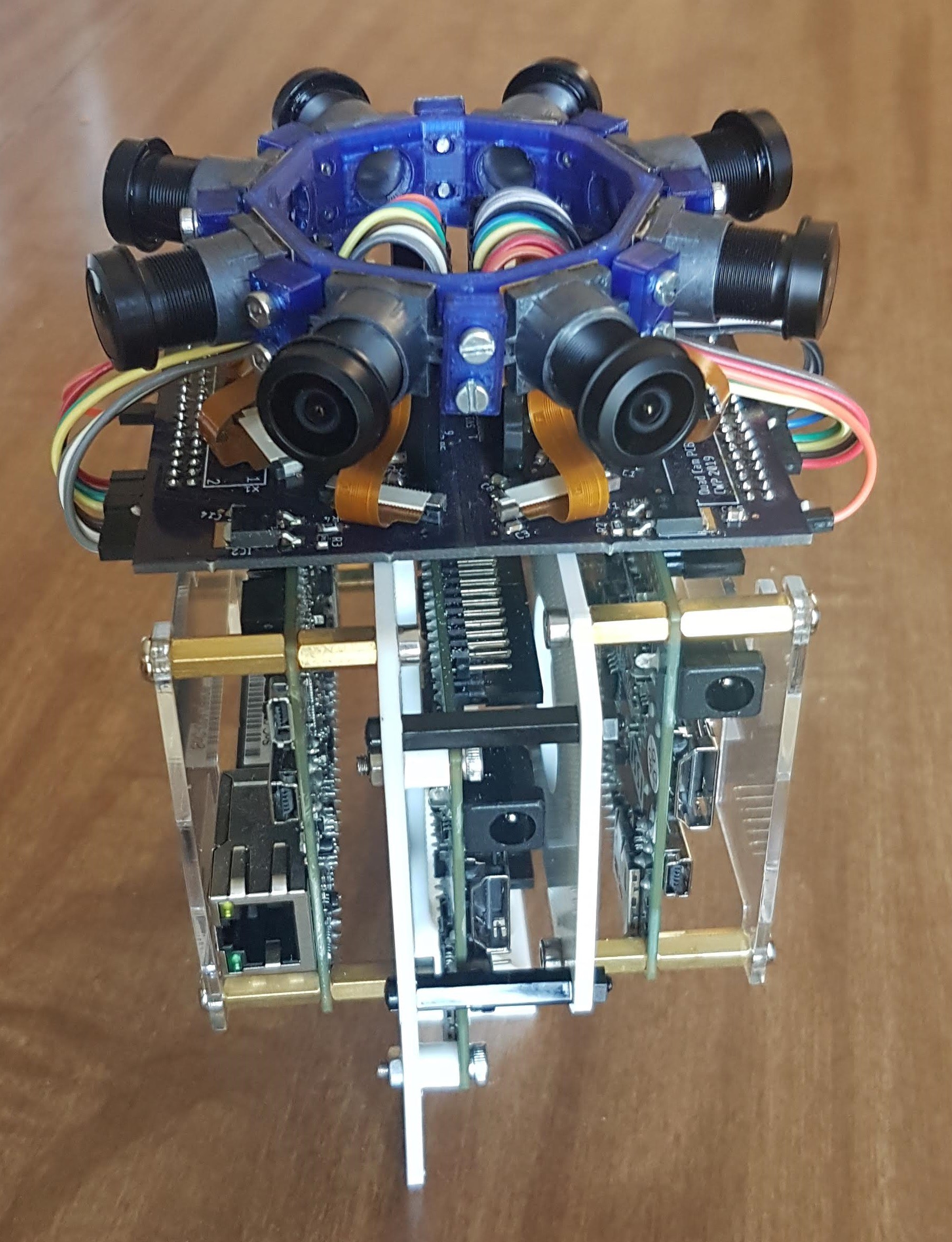
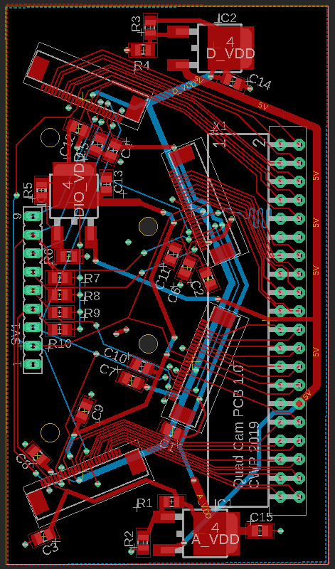
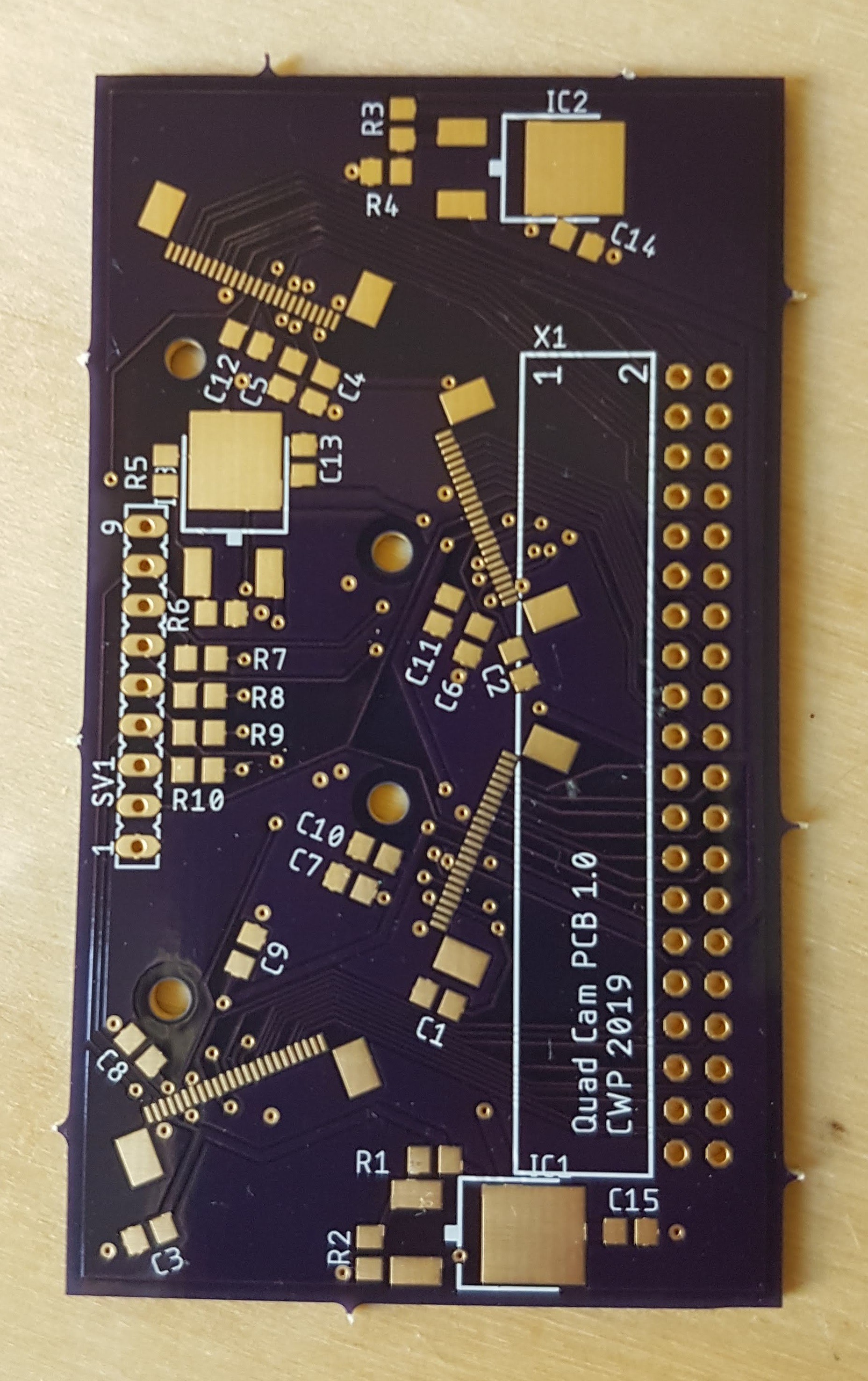
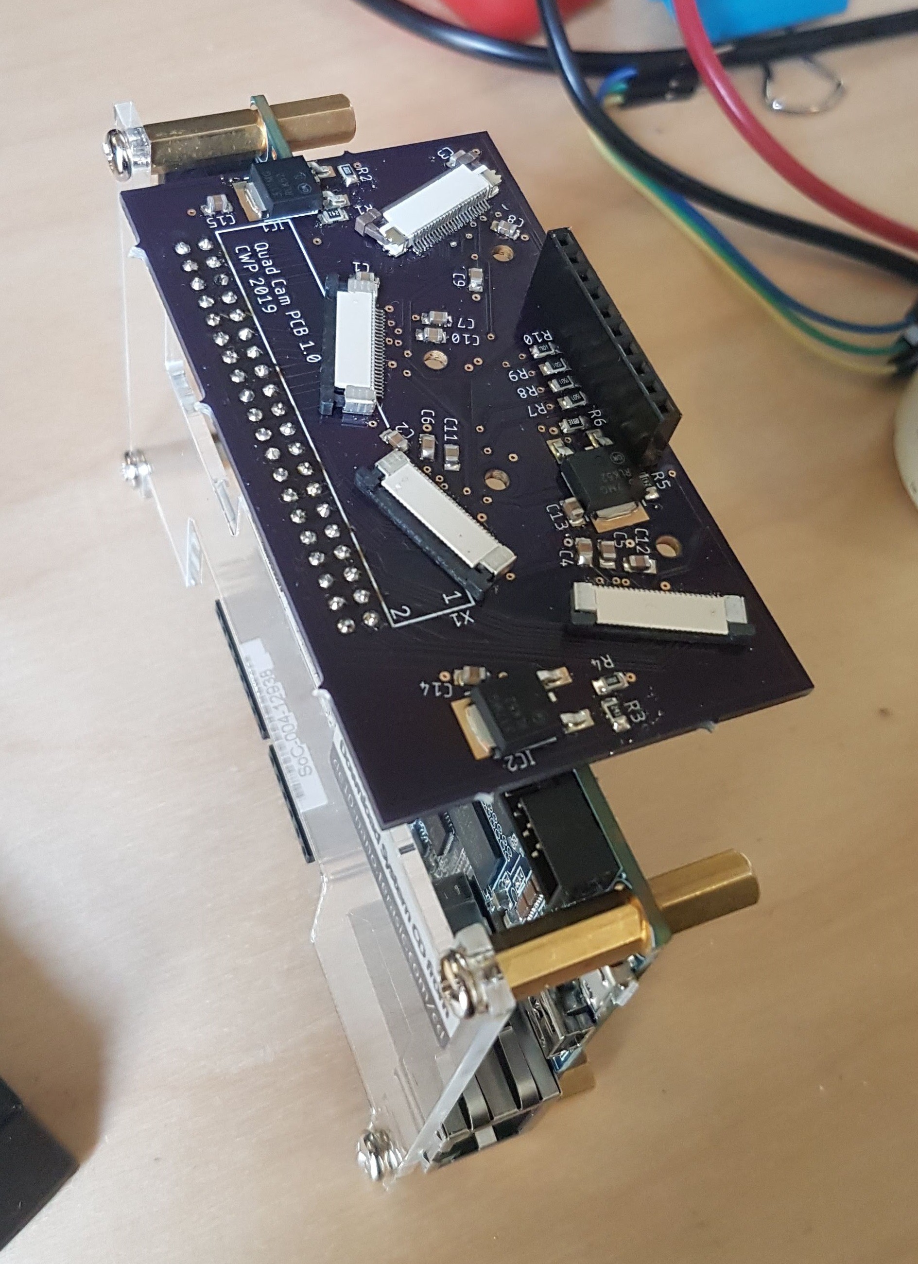
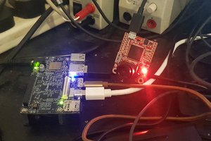
- Camera interface PCB
In progress/partially working:
- Block matching optical flow
- Grayscale conversion and downsampling
- Optical flow filtering
Not yet started:
- Jetson encoding software
- Image stitching modules (uses optical flow map to shift pixels and create interpolated views between cameras)
- Data interfaces between FPGAs and FPGA -> Jetson (either use MAX 10M50 dev boards or some other parallel-to-CSI device)
Off-site resources
Image warping FPGA module GitHub repo
Block matching FPGA (the middle one) GitHub repo
C++ Code that runs on the image warping FPGA SoCs GitHub repo


 alex
alex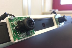
 Adam Taylor
 x-labz
Hi, I am interested in building the project! Did you make any further progress? Thanks!