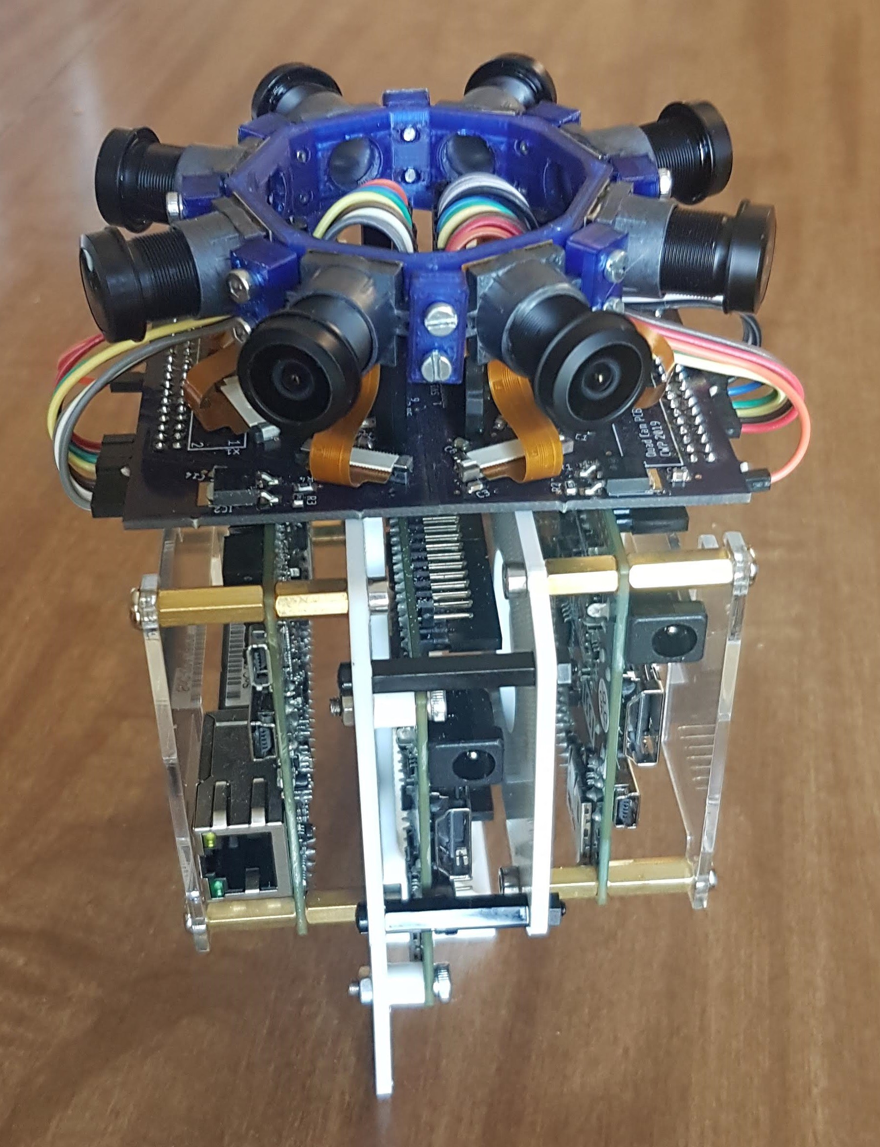
-
Progress on the important stuff
01/18/2021 at 01:02 • 0 commentsTo continue my last post, I'll share the progress I've made on getting the camera closer to doing what it's supposed to. What follows is a technical description of how the system that I've been building works.
Grayscale image to single-bit pixels
The block matching FPGAs receives 8-bit grayscale images from each of the two remap FPGAs over a simple 8-bit parallel bus. This is a total of 8 images, 4 per remap FPGA since they each have 4 cameras. These grayscale images are downsampled by 2x in each dimension from the color image resolution. They are cropped vertically so they are only 90 degrees tall rather than the full 180 that's captured in color. Since they are 135 degrees wide, and the full-res image is 360 degrees and 3840 pixels wide, that means the dimensions are (135/360) * 3840 / 2 = 720x480 pixels.
Recap of 3D image stitching/block matching/optical flow
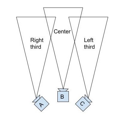
We slice these grayscale images into 3 vertical sections: left, center, and right. Each of these thirds is a 45-degree slice of the full 360-degree horizontal image. Because we have 8 cameras that are distributed equally, that means our cameras are angled at 360/8 = 45 degrees from one another. From this, we know that if we have cameras A, B, and C arranged like so:
![]()
Then the right third of camera A, the center of camera B, and the left third of camera C must all be pointed in the same direction. If they're all looking at something that's an infinite distance away, all three of those slices should be the exact same image. However, we want to show depth in our output images. Therefore, we'll use the left third from camera C and the right third from camera A for the images that we feed to the right and left eyes of the viewer when they're facing in that direction, respectively. As the viewer turns their head to the left, their right eye will go from seeing the left third of camera C to the left third of camera B. Since these cameras are in different locations, that can result in a strange-looking transition between the two images, as nearby objects will be shifted to the right in images from camera B compared to images from camera C. To blend the images, we want to calculate the offset between the positions of objects in the left third of C and the center of B, and then we can shift those objects in the output image to blend the two images together as our final output image transitions between cameras.
I'm doing this optical flow calculation using block matching, where you select the a block of pixels from one camera and search for a matching block of pixels in the image from another camera. Ideally, the block with the least differences will be the same object as the original block.
Back to the main topic: block matching optical flow
To run block matching as fast as possible, I'm converting the grayscale images to images with one bit per pixel. This is done by creating a filtered version of the grayscale image, where each pixel is the average of a 16x16 block of pixels around it, and then comparing each pixel in the grayscale image to the local average at that point. If it's above it, the bit pixel is 1 and otherwise it's 0. This should preserve edges and details while simplifying the image as much as possible. Then, to do block matching we just do an XOR of the original block to the candidate block and count the bits, otherwise known as calculating the hamming distance.
This works for areas of the image with the right amount of detail, but completely fails on areas with no texture or repeated patterns (walls, floors, etc). We want to save the block matching results that are correct and discard the ones that are just random noise. How do we do that? My method assigns a confidence score to each block match. Right now, this confidence is just the minimum (best) hamming distance minus the average hamming distance for all the blocks that we tried to match to. This actually works surprisingly well to predict how good a block match is. See the results below:
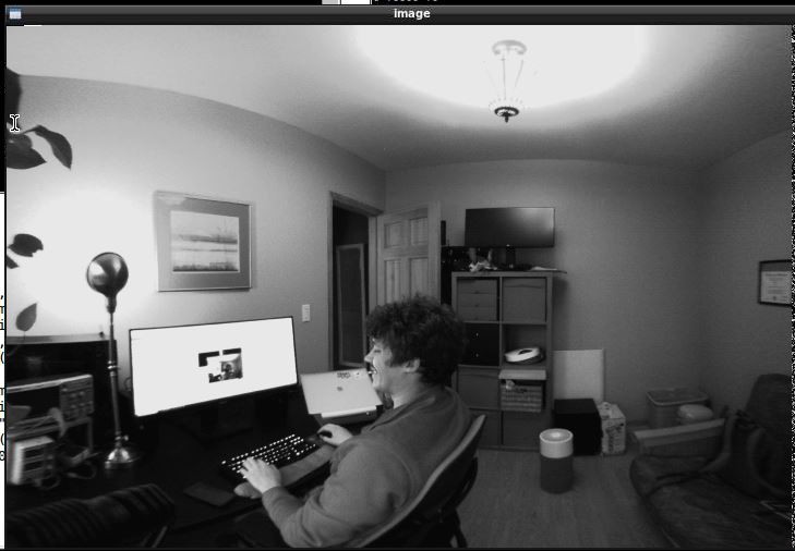
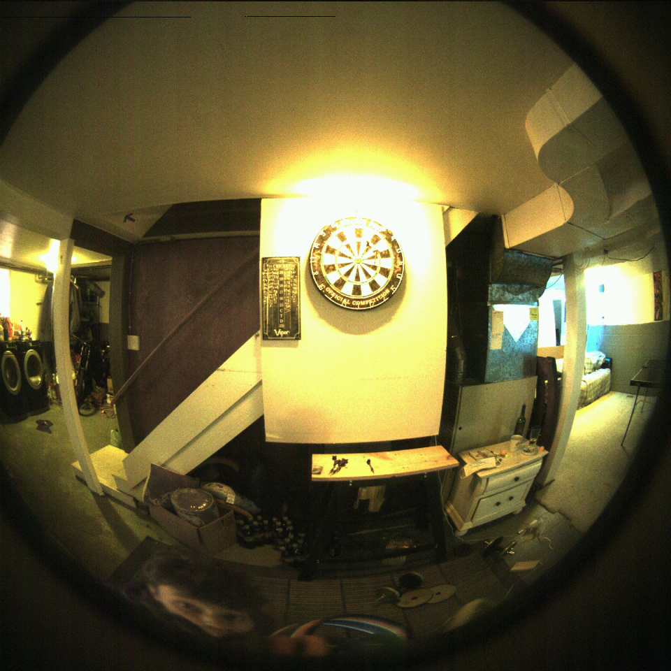
Above: The full 135-degree wide grayscale image from the center camera. We receive this from the remap FPGA
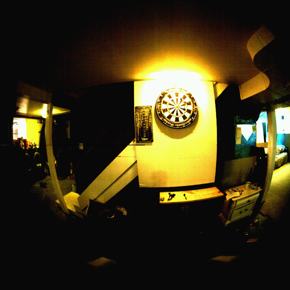
Above: The center third (45 degrees) from this converted to 1-bit pixels
Above: The depth and confidence. This one requires some squinting to interpret.
On the left is our depth output, with darker pixels being closer. The black pixels at the top are completely wrong - those are the ceiling which doesn't have enough texture to figure out the depth. The gray blob in the lowerish center is me, and I'm darker than the surrounding pixels since I'm closer to the camera than the background is. On the right is the confidence. As you can see, the wall and ceiling are darker than the detailed areas. This means our confidence is lower, which it should be, since the depth estimates there are totally wrong.
What's next?
What I'm working on now is how to process the depth and confidence, preserving depth in high-confidence areas and propagating that to lower-confidence areas. Once that's working, we need to upsample and stream the depth back to the remap FPGAs so they can use it to stitch the color images!
-
Slow but steady
01/17/2021 at 22:03 • 0 commentsI recently picked this project up in November after a year or so of little to no progress. I'm happy to say that while it's not taking videos yet, I've made some good progress towards that goal. Here I'll list some of the updates I've made and try to throw in some pictures to keep your attention.
Turned the image sensors sideways
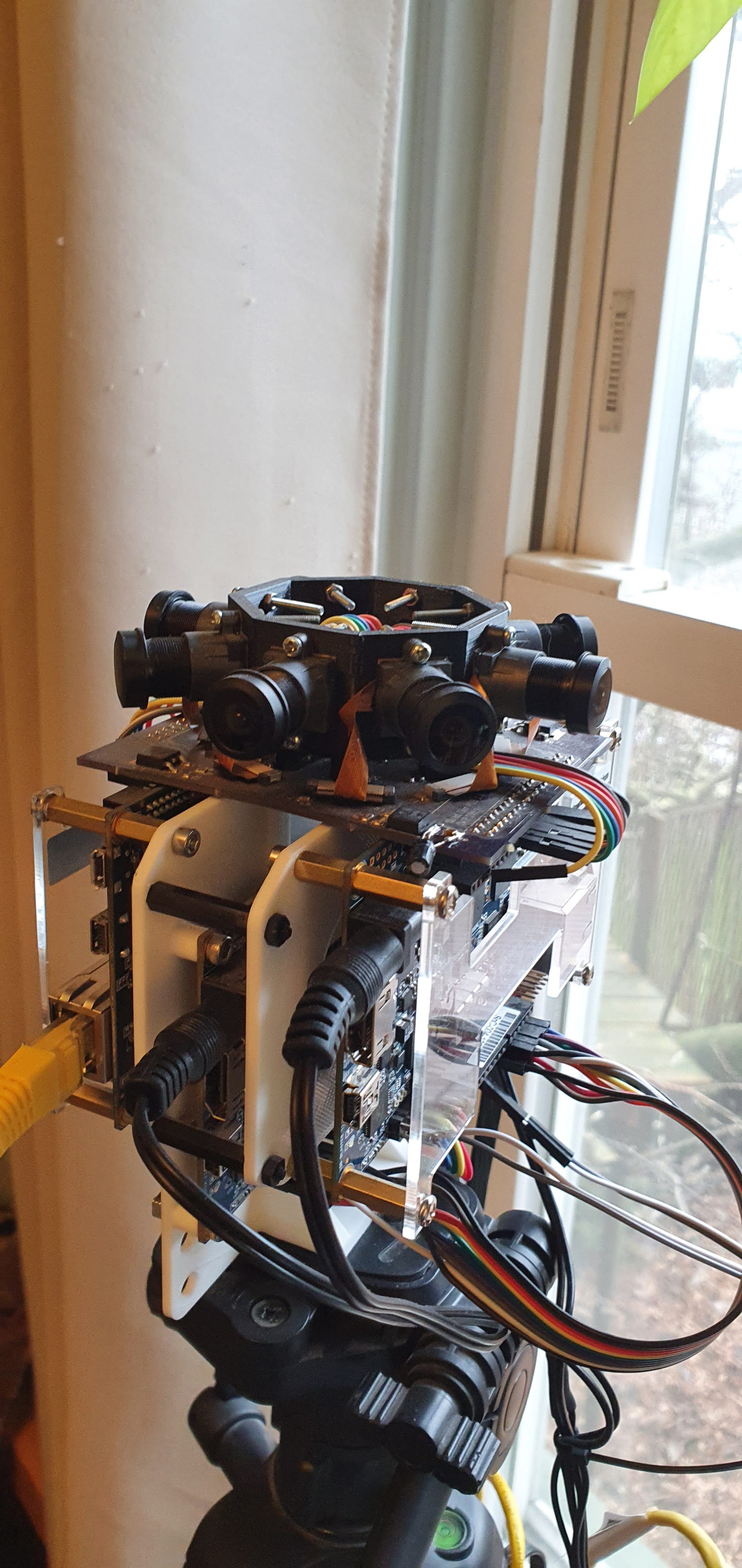
As it turned out the way I originally mounted the AR0330 image sensor modules had them sideways, so the image was longer in the vertical direction than in the horizontal. At first I thought this would be okay, but I quickly realized that with the 1.44mm focal-length lenses I'm using, the image circle is too large so I have less than the required 135 degrees of horizontal FOV if the image sensor is portrait-oriented. To rectify that, I printed a new camera bracket that you can see here. The ribbon cables get a little kinked but luckily none of them have displayed symptoms of reduced connectivity.
![]()
Power stuff and PCB fix
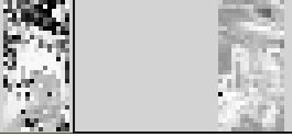
Ever since I put together the camera I've noticed an odd issue where images from some of the image sensors would have very low dynamic range, or have rolling stripes of darkness/lightness:
![]()
Above: Good one. Below: bad one.
![]()
I recently got an oscilloscope and decided to do some probing. Turns out that the analog power supply to the image sensors (AVDD) was having some major noise issues at the image sensors that were farthest from the linear regulator that supplied it. Makes sense, as I made the supply traces pretty thin to those last couple cameras. I expected too much from those tiny ceramic capacitors I guess. Adding an electrolytic capacitor to the PCB across AVDD helped a lot. There are still some barely visible image quality issues but probing the supply voltage shows that it has gotten a lot cleaner.
I also decided to replace the 3 different 5V wall warts that I was using with a single 5V supply. This turned out to be a terrible idea at first, as the parallel busses between the FPGAs were causing major ground loops that didn't occur before since the supplies to each FPGA was isolated. However, shortening the power supply wires seems to have mostly fixed it.
Grayscale image transfer fix
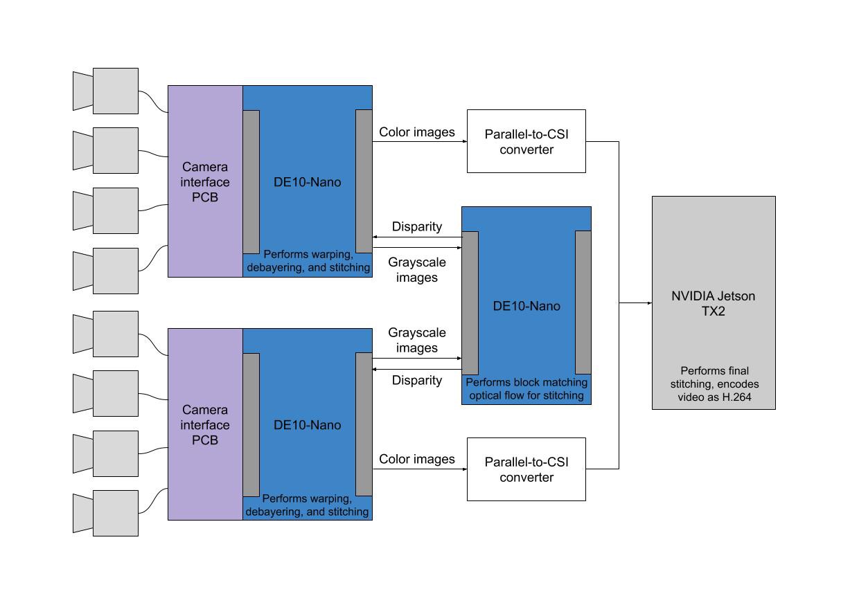
As shown in the dataflow diagram for the project, there are two FPGAs that receive and warp color images from 4 image sensors each. They downsample and grayscaleify the color images and send them to the center FPGA, which is responsible for calculating the optical flow of the images (stereoscopic depth estimation, pretty much). This pipeline was sort of working but mostly not. It would get hung up and miss pixels or entire frames quite frequently. Turns out a major issue was that the remap FPGAs (ones that are connected to the cameras) were reading the grayscale images from DDR3 with a burst size of 16. The FIFO held 128 entries, which seemed like plenty. However, what I didn't realize was that the DDR3 slave interface supports up to 14 pending reads, so in rare cases, there could be 14 bursts of 16 words that came in all at once, overflowed the FIFO, and caused output pixels to be missed. Fixing that made it all happy again.
Quality of life stuff: VNC, code cleanup
A lot of the work I've done has centered around making it easy to work on the camera. I started by hooking up all the FPGAs to the internet so I could install VNC and remote into them rather than having to manually plug an HDMI cable and mouse and keyboard into each one to access the Linux GUI running on the SoC. For the remap FPGAs, I just hooked them up to ethernet and they worked, after following these instructions to set a static MAC and install VNC:
https://community.intel.com/t5/Programmable-Devices/MAC-Address-changes-on-reboot/td-p/124962
https://techloverhd.com/2015/05/install-lxde-vnc-gui-on-ubuntu-debian-server/
The middle FPGA was a whole 'nother story. When I made the 3D printed frame, I neglected to leave enough room for the ethernet jack. 2019 Colin decided I would never use the ethernet jack, so rather than just printing a new frame, I should just pull it off. 2020 Colin was very upset by his predecessor's poor decision but figured he'd just get a microUSB to ethernet adapter, and purchased the first one on Amazon, without thinking to check driver support. Several days of struggling and crying with kernel panics and confusion ensued. Don't be like 2019 Colin or 2020 Colin. I finally gave up and bought a mt7601u Wifi adapter since there is a driver called "mt7601u" in the LXDE kernel tree. It worked, and that terrible saga came to an end.
Another effect of putting the FPGAs on the network is that now I can just scp new bitfiles to them from my PC, and no longer have to manually remove the MicroSD cards and copy them over.
I also have all the C++ code on the FPGAs in a github repo, making it a million times easier to edit and keep in sync between the FPGAs rather than having to edit in a 1280x720 window in the LXDE GUI.
I also refactored the github repo for the remap FPGAs so there's less random Quartus artifacts and hopefully just the files that are needed to open the Quartus project, generate the IP, and build the FPGA. I haven't tested that yet though.
More stuff
That begins the list of things I've done. I'll continue with another, even more exciting project log.
-
Frame
07/20/2019 at 02:14 • 0 commentsI've been working on the HDL side of things for a while, getting the block matching and remapping working well. I thought it would be nice to switch things up this week and finally make a proper frame that holds the third FPGA board, which will perform the block matching and depth map filtering. You can see the updated design in my OnShape document: https://cad.onshape.com/documents/e230395963de661bfa5c14c7/w/05d75a95b60ee2972e714205/e/a708f4a0d0e872dd361e0a75
![]()
![]()
-
Camera Interface PCB
04/27/2019 at 23:38 • 0 commentsThe camera interface PCB connects the DE10-Nano GPIO to 4 AR0330 modules and provides the power rails for the image sensors. My main design objectives were to keep the connections between the cameras and DE10 as short as possible to maintain signal integrity, and to mount the PCB perpendicular to the DE10 PCB so it would stay out of the cameras' field of view as much as possible.
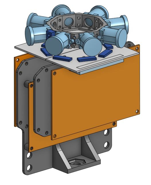
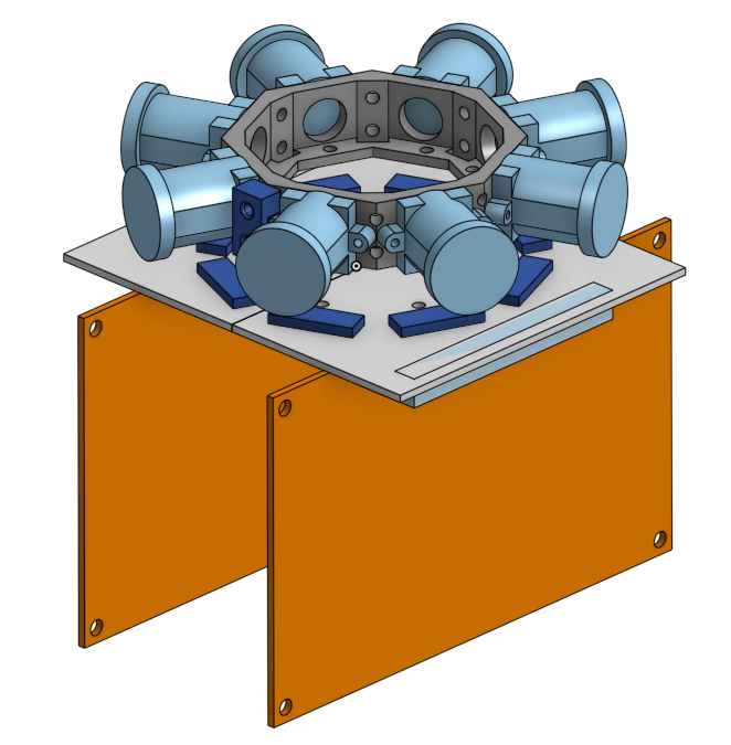
To create seamless stereoscopic images, the 8 camera modules have to be laid out in an octagon with 64mm between every other camera's center of projection. I used OnShape to design a camera mount and sketch a PCB to attach to the mount and connect to the cameras. You can access the OnShape document here.
OnShape screenshot. Dark gray is the mount, light gray is the PCB, light blue is the camera modules, and orange is the DE10-Nanos. From OnShape, I exported the PCB shape, mounting hole locations, and connector positions as a DXF for use in Eagle. Ideally, I could route all of the camera connections through the 40-pin right-angle header and have only one connector to the FPGA board. Unfortunately, there are 36 available pins (4 for power and ground) and 4 cameras, leaving only 9 pins per camera. The parallel bus on each camera has an HSYNC, VSYNC, PCLK, and 10 pixel data lines. PCLK and HSYNC are the most critical to getting valid pixel data, so I opted to put these on the main header along with 7 bits of pixel data. 7 bits is far from optimal but the colors are going to be converted to 16-bit RGB with 5 bits per color so I don't think it makes much of a difference. The rest of the connections, VSYNC, XCLK (camera clock input), SDA, SCL, and RESET, are all on another header that connects via jumper wires to the DE10-Nano Arduino IOs.
I ended up assembling the PCB using solder paste and a hot plate for the SMD parts. The camera connectors were surprisingly easy, requiring a bit of rework but a lot less than I experienced the last time I soldered this type of connector.
Check out the Files section of this project for the PCB EAGLE project and BOM.
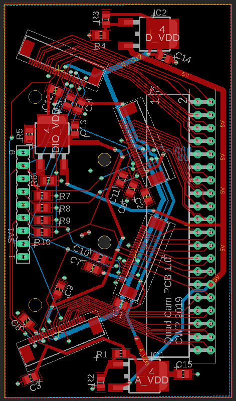
PCB design in EAGLE ![]()
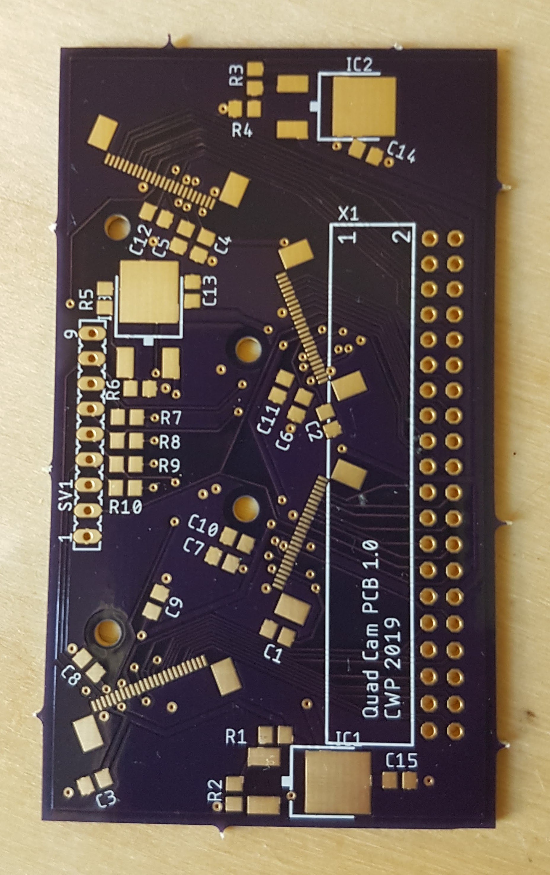
Unpopulated PCB from OSHPark ![]()
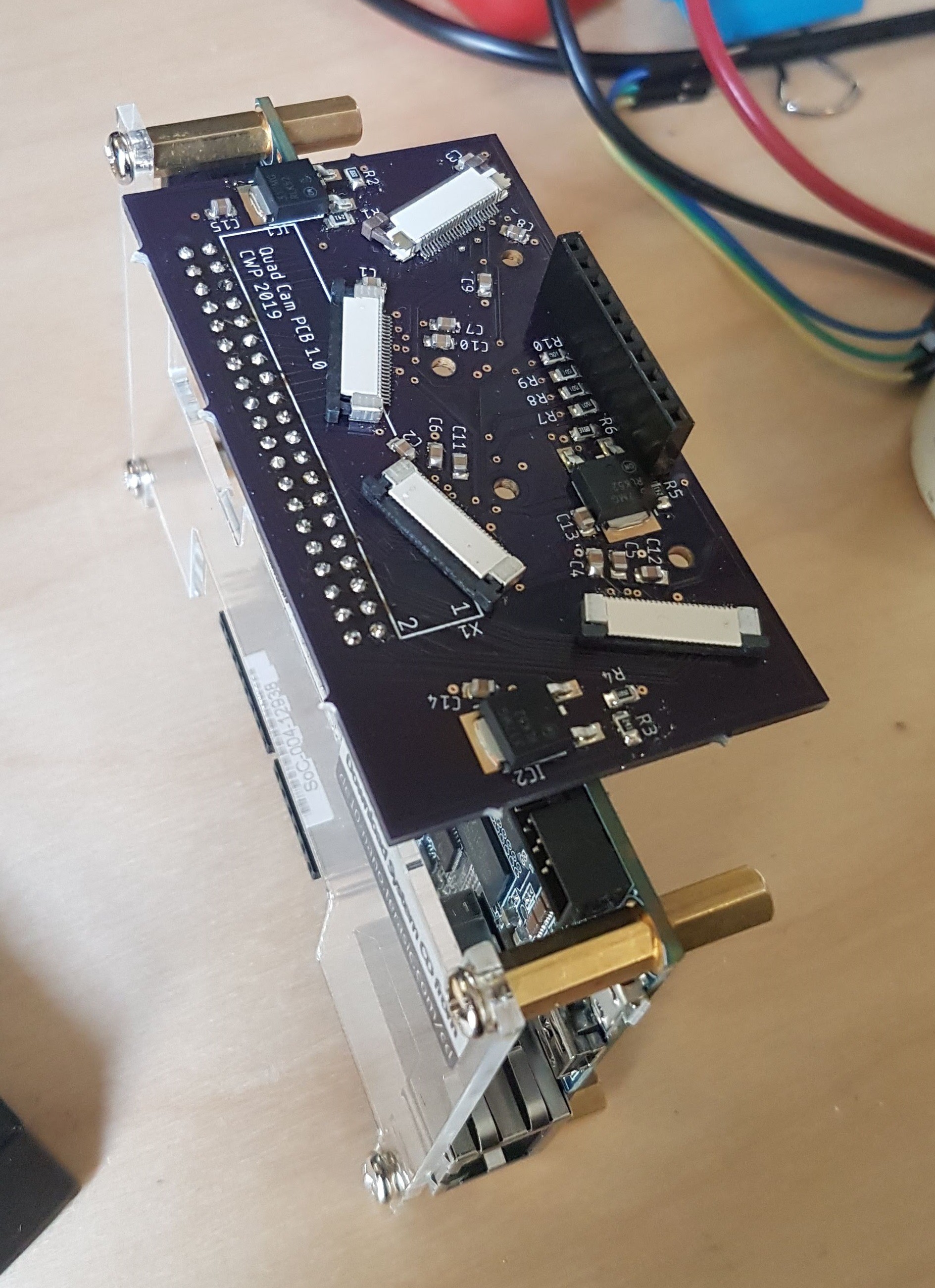
Fully populated PCB, mounted on the DE10-Nano ![]()
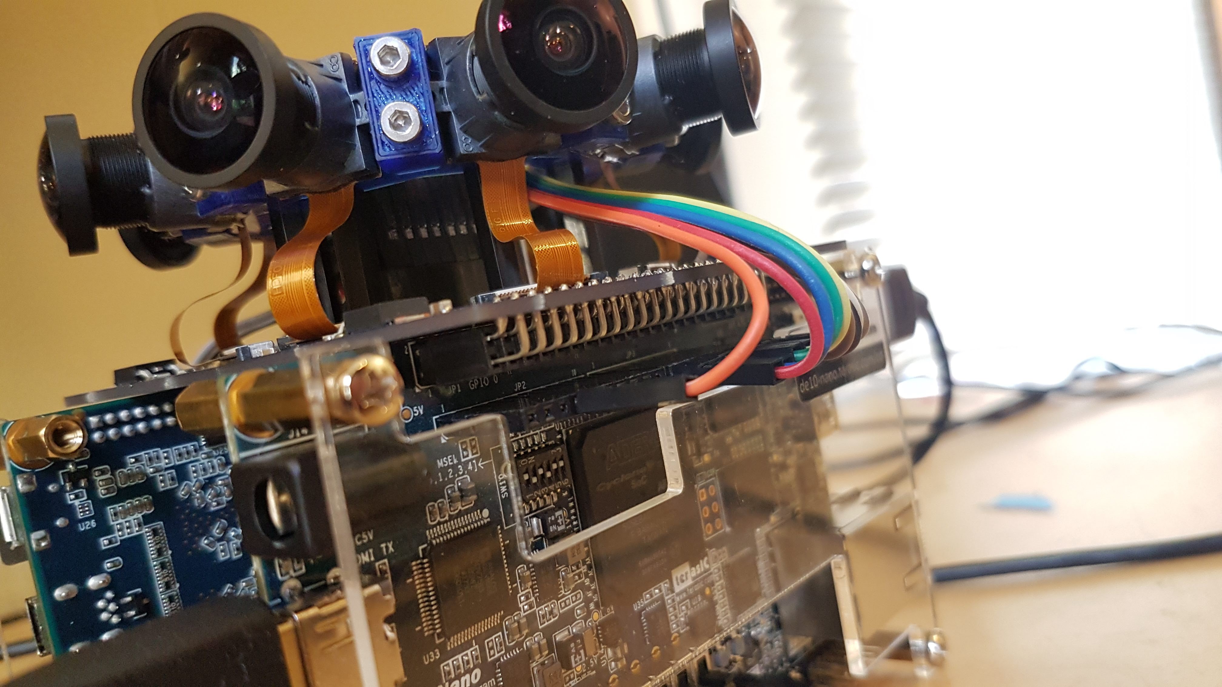
Right-angle 40-pin female header on the underside of the board to connect to the DE10-Nano GPIO header. The colored wires are the signals that didn't fit on the main header. -
Dataflow
04/27/2019 at 21:41 • 0 commentsThe figure below shows the system diagram I came up with after running the numbers on the system requirements. The DE10-Nano is still the centerpiece of the camera due to its high number of IOs, strong FPGA, and low price. I debated using the Ultra96 board, which has high speed connectivity, a faster memory bus, and more powerful Xilinx FPGA, but it wouldn't be able to support input from 4 cameras simultaneously and costs $200 compared to $130 for the DE10-Nano.
![]()
So far, I have the front end of the camera mostly working - the PCBs are assembled, and two DE10-Nanos are successfully talking to the cameras and performing debayering and warping.
-
Specification/Initial Design
04/26/2019 at 22:57 • 0 commentsBuilding my first 360 camera was extremely instructive of the difficulties and pain points of capturing immersive VR content. After crafting the image capture modules for the FPGA and creating stitching software for my desktop PC, I realized that capturing video and performing stitching on-board in real time would require an exponential increase in system complexity. To meet this challenge, I started by choosing my goal specifications and redesigning the camera from the ground up.
Specs
- Output format: 3840 x 3840 @ 30fps, 3840 x 1920 per eye
- 8 cameras
- No audio recording on board, to keep things simple - all videos will be accompanied by a fitting orchestral score to be performed at the time of viewing
- Ideally keep cost under $1k
Image Sensors
The image sensor I previously used, the OV5642, was great for its ease of use and resolution but the output interface limited it to 5fps of full resolution output. In my search for an inexpensive replacement, I found this $15 module with the Aptina AR0330, capable of outputting 3MP at 30fps through a simple parallel interface, just like that of the OV5642.
Processing
The logic on the FPGA needs to be significantly more complicated than the modules in the previous version, which simply stored the incoming raw pixel stream into the DDR3 RAM, where the ARM HPS read the image buffer and saved it to the MicroSD card. High-speed image processing tasks like this require a great deal of memory bandwidth and processing power. To power the full warping and stitching pipeline, I designed a setup using 3 DE10-Nano boards. 2 of the DE10 Nanos run identical logic, each one receiving images from 4 image sensors, debayering, and warping the images to the spherical projection required for VR viewing. The third DE10-Nano receives downsampled grayscale versions of the camera images from the first two FPGAs. It performs block matching on these grayscale images to get disparity maps, filters the disparity maps, and sends them back to the other FPGAs to be used for stitching.
Encoding
From my research, it seemed that the Jetson TX2 was the best option and only reasonably price embedded device capable of encoding 4k video at 30fps. The fastest and most efficient way to get image data onto the Jetson is through its 12-lane MIPI CSI-2 camera interface. Unfortunately, the DE10-Nano doesn't have pins that can be configured to be used as CSI transmit lanes. Because of this, it'll be necessary to insert an intermediate parallel-to-CSI image conversion device. There is at least one chip (Toshiba TC358748XBG) designed for this purpose, but it's in BGA format - meaning it'll require an expensive and hard-to-assemble PCB - and doesn't appear to be regularly stocked. The simplest option seems to be using the Intel MAX 10M50 development board, which has 3.3V IO pins that can talk to the DE10s and a built in MIPI CSI-2 transmit PHY. I'll need at least 2 of these, since they have 4 TX lanes each.
VR Camera V2: FPGA VR Video Camera
An FPGA-powered camera that shoots and stitches stereoscopic 360 video in real time.
