-
Moving the project to Digilent Cmod-A7!
08/13/2019 at 12:52 • 0 commentsWhew! Apologies for the long delay - I was working on this on-and-off, and struggled on the new Digilent Cmod-A7 I got in a cheap price from a local store (they are doing stock clearence).
Unfortunately, I had been also wrestling on the Xilinx Vivado toolchain, and it looks like it hasn't been quite nice to me. I've asked around in Digilent, and lucky me they are helpful enough to get a simple project to be compiled: https://forum.digilentinc.com/topic/18479-cmod-a7-vivado-2019-cannot-get-past-implementation/
Also, unlike the Intel Quartus ones, I couldn't add 74 logic blocks inside their system board, and had to fabricate my own 74245 + 74373 glue logic in Verilog instead.
Even compiling it could be painful - 5 minutes and I ended up simulating on the most part of the design. Finally, I got this to catch the lower address without using 74373 and 74245! (all inside the FPGA)
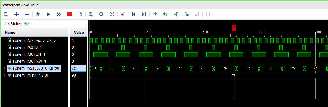
All is not done yet, and I'm doing my best to make it run a simple program. As usual, the logic analyzer output shows the 8088 reading 0x90 (NOP) from FPGA and the FPGA latches the bottom half of the address each strobe.
Note: For the previous log, I had found out that Cyclone 2 doesn't have libraries or Nios part to directly connect the SDRAM to some other peripherals. This only exists in newer Cyclone models, so I had to use the Digilent Cmod-A7 I got from a stock clearance sale instead.
-
Cyclone 2 Nios 2 - A little diversion!
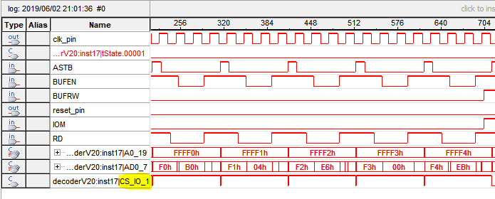
06/02/2019 at 13:16 • 0 commentsWhew! I have got the chip select to work finally - all I need to do is to put the address in the "always" block:
always @(A0_19) begin
	if(A0_19 >= 20'hffff0 && A0_19 <= 20'hfffff)
		CS_IO_1 <= 1;
	else
		CS_IO_1 <= 0;
end
At the least, when it resets, it goes back to the same address and the same instructions instead of going everywhere in the last experiment:
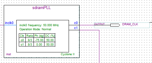
Since I can get it to be selected, what if I try to connect this to an SDRAM? Sounds like I'm wrestling with a grizzly bear. Or maybe not. Hmm, I can try to dump some stuff into the SDRAM as a start. Fortuntately, I still have the old copies of the sample codes when I purchased the ASK2CB. However, I got into a big roadblock - getting this to compile, and even getting this to be programmed into the SDRAM is a big issue too! That old codes which have the NIOS only worked in Quartus II 12 and below, and I'm using the last version 13, so I have to port that whole project into Qsys.
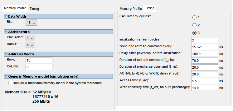
And that's isn't fun, I admit. I couldn't even convert the thing without getting errors during compilation and etc. I have to create that project again, and used these SDRAM values I got from the old codes:
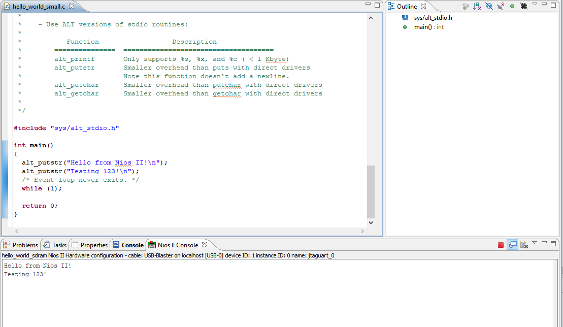
It is extremely tedious! After a whole evening, I got this to work finally:
Of course, that doesn't end here. I'm writing a simple loader program that loads stuff from the PC to the SDRAM on that board. And here are the updated NIOS 2 project template too, if you do not feel like creating the whole project again. (The project template is in the files section: nios_sdram_ASK2CB)
-
Running short fragment of program - but needs a lot of fixing!
05/26/2019 at 14:42 • 0 commentsI have squeezed some simple instructions into a 16-byte ROM that writes 0x04 into the I/O address 0x00, and repeats (http://www.homebrew8088.com/):
A:
MOV AL, 04
OUT 00, AL
JMP A
This is then converted into machine code (https://defuse.ca/online-x86-assembler.htm), and I write this in the *.mem file that the Quartus 2 can deploy into the array (https://timetoexplore.net/blog/initialize-memory-in-verilog):
module storageReadOnly(output [7:0] data, input [19:0] addr, input RD);

reg [7:0] memory16bytes [16:0];

initial $readmemh("rom_image.mem", memory16bytes);

assign data = memory16bytes[addr & 20'h0000f];

endmodule
The "rom_image.mem":
B0 04 E6 00 EB FA
And here it runs:
However, the decoding part isn't the most straightforward thing to write in Verilog. I'm not even sure if my version of decoding could work:
always @(negedge ASTB) begin
	if(A0_19 >= 20'hffff0 && A0_19 <= 20'hfffff)
		CS_IO_1 <= 1'b1;
	else
		CS_IO_1 <= 1'b0;
end
This CS_IO_1 is a temporary chip-select to select an I/O address which I will connect these to the LEDs later to verify the operation. I'll expand on the V20 writing to the FPGA after this.
-
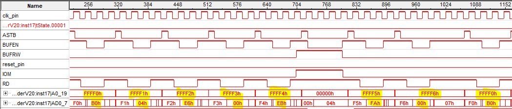
A8-19: Can be seen too!
05/25/2019 at 15:48 • 0 commentsAfter connecting all these wires from the V20's A8-19 to the FPGA and quickly turn on the SignalTap, it's already known that it is starting from the reset vector 0xF_FFF0.
My next step is to have these connected to a simple, small 16-byte memory block and run a short piece of code there.
-
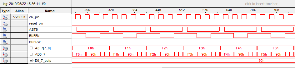
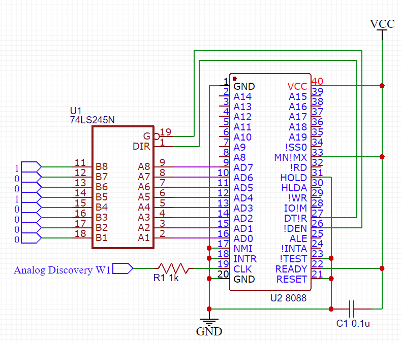
AD0-7: Address grabbed.
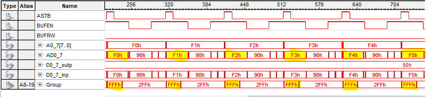
05/22/2019 at 13:45 • 0 commentsI have added a 74373 into the Quartus 2 BDF on the inputs of the 74245. And yes - it grabs the first 8 bits of the address.
I have even placed a 0x90 opcode for the processor to read - and at least, it looks like it now starts from the reset vector.
The top bits of the address - gonna connect these afterwards. Hopefully it's the 0xFFFF0. :)
![]()
-
AD0-7: Me trying to grab its address first!
05/20/2019 at 15:08 • 0 commentsLucky me I have a bit of a long holiday here and I managed to have the FPGA to grab the address from the AD0-7 first. The bad news is, the FPGA couldn't grab anything on the address. Going back to the basics and to further understand how this 8088 works, I wired up the extra 74373 on top of the 74245, with reference to http://www.homebrew8088.com/:
And when I connected the first four bits on the 373's Q0-Q3, I'm getting this:
I'm suspecting that it's working alright, since the address is counting upwards (the 8088 starts at address FFFF0).
The more tough part is I do not have enough pins on the FPGA board's connector to even connect that latched address A0-A7, so I'm cooking up some method on how I could effectively make this run properly without adding even more stuff on top of it!
-
Back to the drawing board!
05/12/2019 at 14:03 • 0 commentsAfter another weekend on fumbling on why the ASTB that wasn't strobing, I had to take apart the FPGA and the V20, and did some research on it.
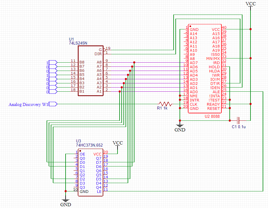
Referring to the page: http://www.vcfed.org/forum/showthread.php?53999-Suspected-fake-counterfeit-NEC-V20-uPD70108HCZ, seems that to get the ASTB to strobe, I had to connect this to a 74LS245. The other port of the 74LS245 is a bit pattern 0b10010000 (x86 NOP instruction). Without the ASTB strobing, the rest of it will not work even if I connect the FPGA to it (this schematic is made using EasyEDA):
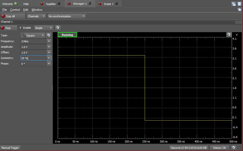
With all the trial-and-error again, I breadboarded everything and connected the clock to the Analog DIscovery 2's waveform generator. Also, the supply is +3.3V because I wanted it to be compatible with the FPGA board.
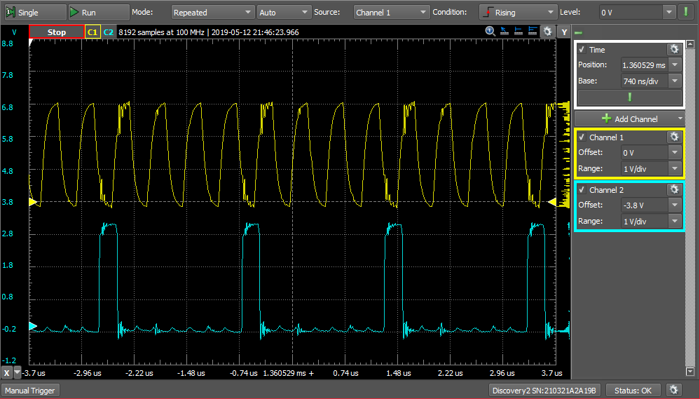
And there's the ASTB strobing! Unfortunately, the noise was terrible and I'm planning to get rid of it as much as possible!
Well, it's at least working, but the challenge is to put this back into that FPGA! No easy task, I'm expecting a lot of roadblocks ahead! :)
-
Oscillator!
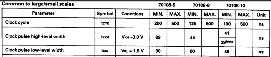
04/28/2019 at 15:06 • 0 commentsAs the title said. Here we are trying to write up a simple oscillator for the V20. It looks like the V20 allows a square wave with 50% duty cycle, as long as you exceed these minimum values:
(NEC V20 Datasheet)
Here is a simple Verilog code for the oscillator:
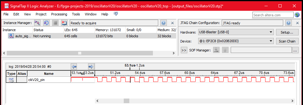
module oscillatorV20(input clk, output reg clkV20);

reg [31:0] counter = 0;

always @(posedge clk) begin

	if (counter == 8'd5) begin
		counter <= 0;
		clkV20 <= !clkV20;
	end
	else begin
		counter <= counter + 1;
	end

end

endmodule
And using SignalTap 2, we see this as an output (this is an example 1 MHz square wave, and I'll tune to the 2 MHz after this):
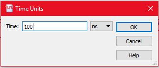
The problem with the little time bar was, I have to manually key in the "Time Units" (right click on the time bar, and click "Time Units"). Enter 100ns inside:
As this is working, my next step will be wiring the thing up to the FPGA board (ASK2CB) and check whether the ALE pin are pulsing or not.
Let's experiment: NEC V20 + FPGA
What happens when you connect a NEC V20 to an FPGA? Let's find out!