-
1Transformer Build
This instruction is for building the transformer. It describes materials and fabrication guidance but assumes the reader has experience assembling magnetics. Additional information can be found in the magnetics zip file and the 'inductors' tab of the Excel design file.
The following materials are required:
- TDK RM14 Power bobbin, mfg #B65888C1512T001, Digikey 495-5341-ND
- TDK RM14 N41 Ferrite core, mfg #B65887E0000R041, Digikey 495-5335-ND
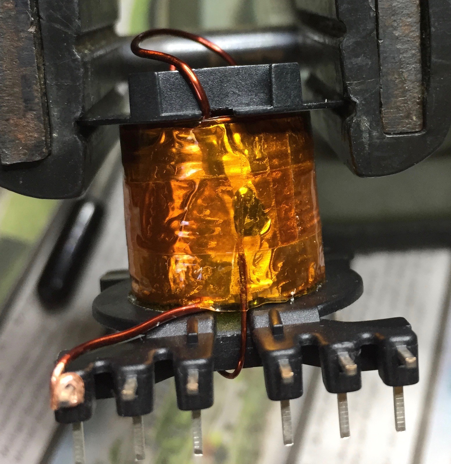
- TDK RM14 clamps, mfg #B65888A2002X000, Digikey 495-5339-ND
- 3M 1mil Polyimide tape 1205 (various widths) or equivalent
- 3M 1oz Copper foil tape 1181 or equivalent (required width = 17mm)
- 20 AWG MW35C HY magnet wire
- 24 AWG MW35C HY magnet wire
The transformer consists of three windings:
- High voltage secondary, N=32 consisting of two layers of 16 turns each, single strand 20 AWG
- Primary, N=2, single layer, 10 strands 20 AWG
- Auxiliary secondary, N=3, single layer, 1 strand 24 AWG
Assembly.
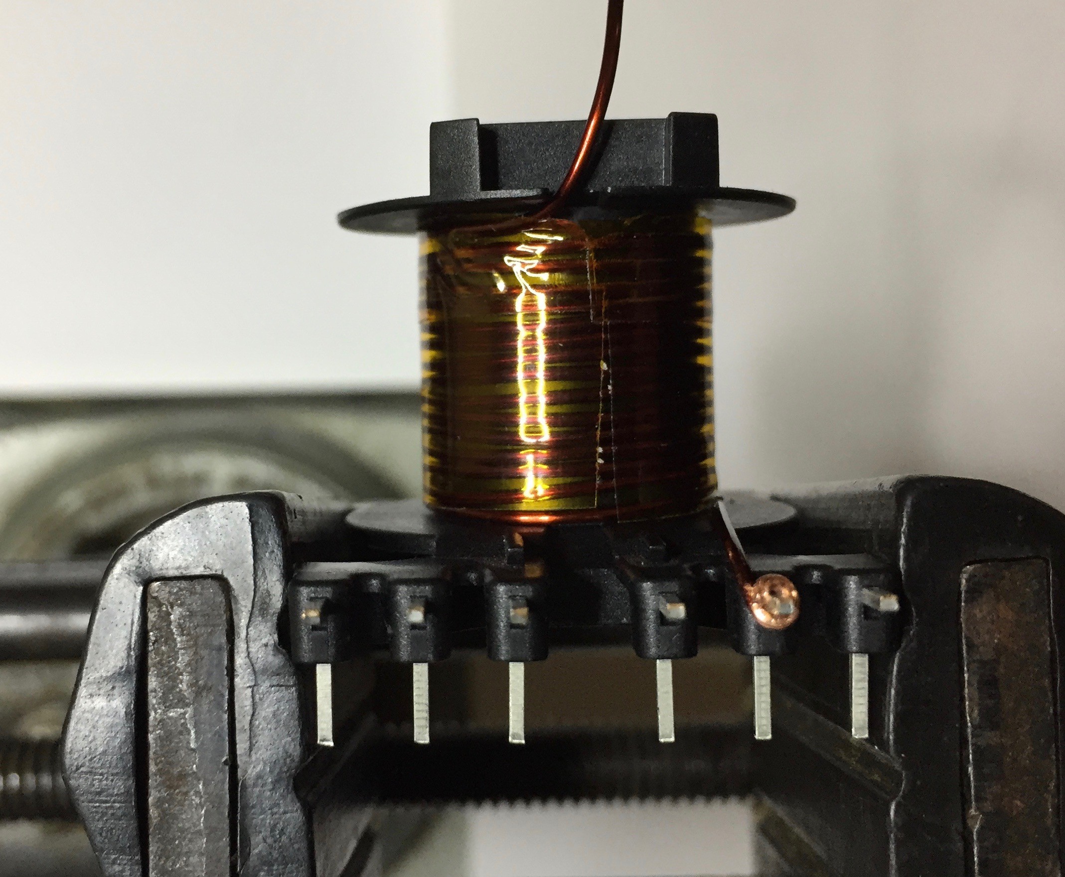
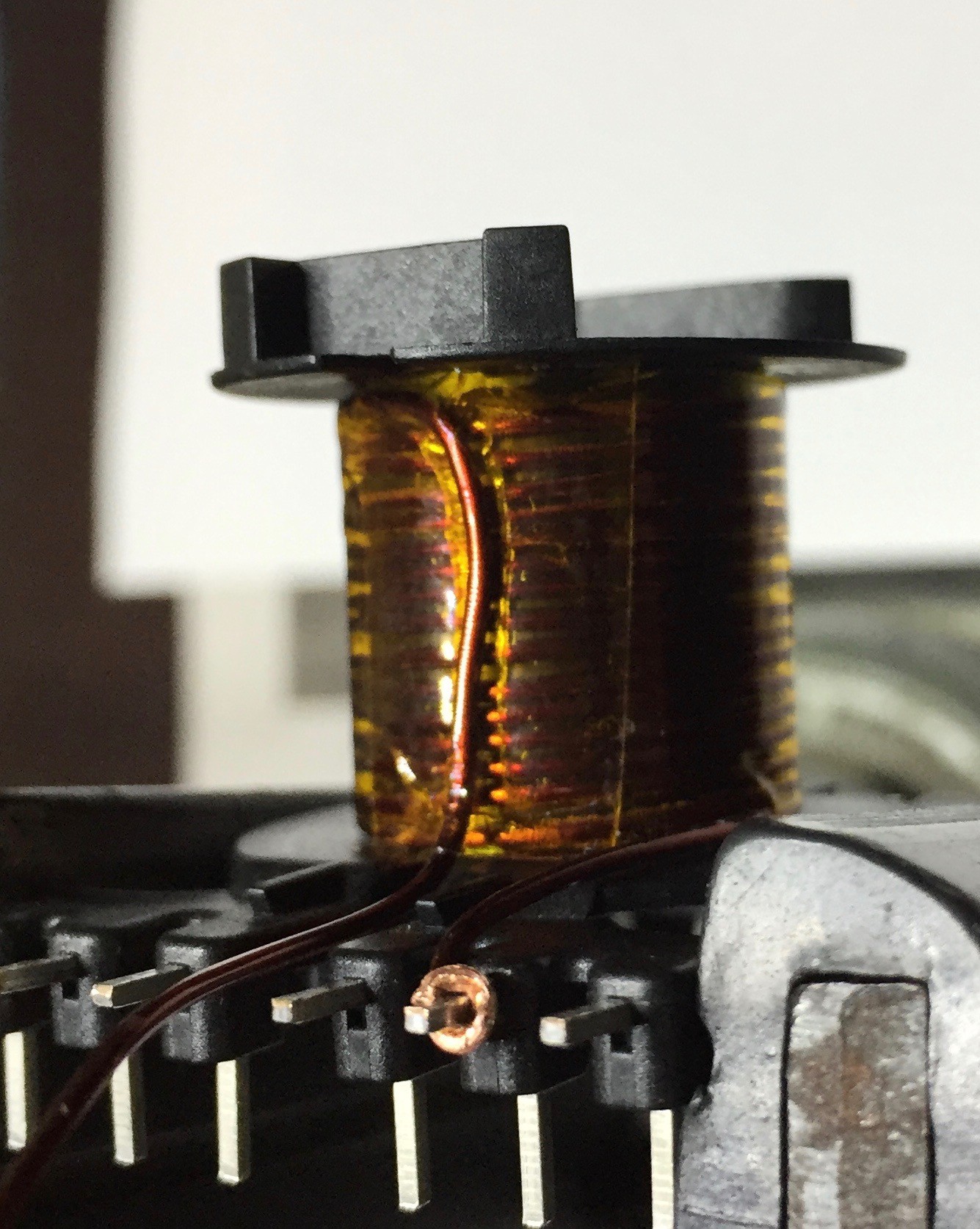
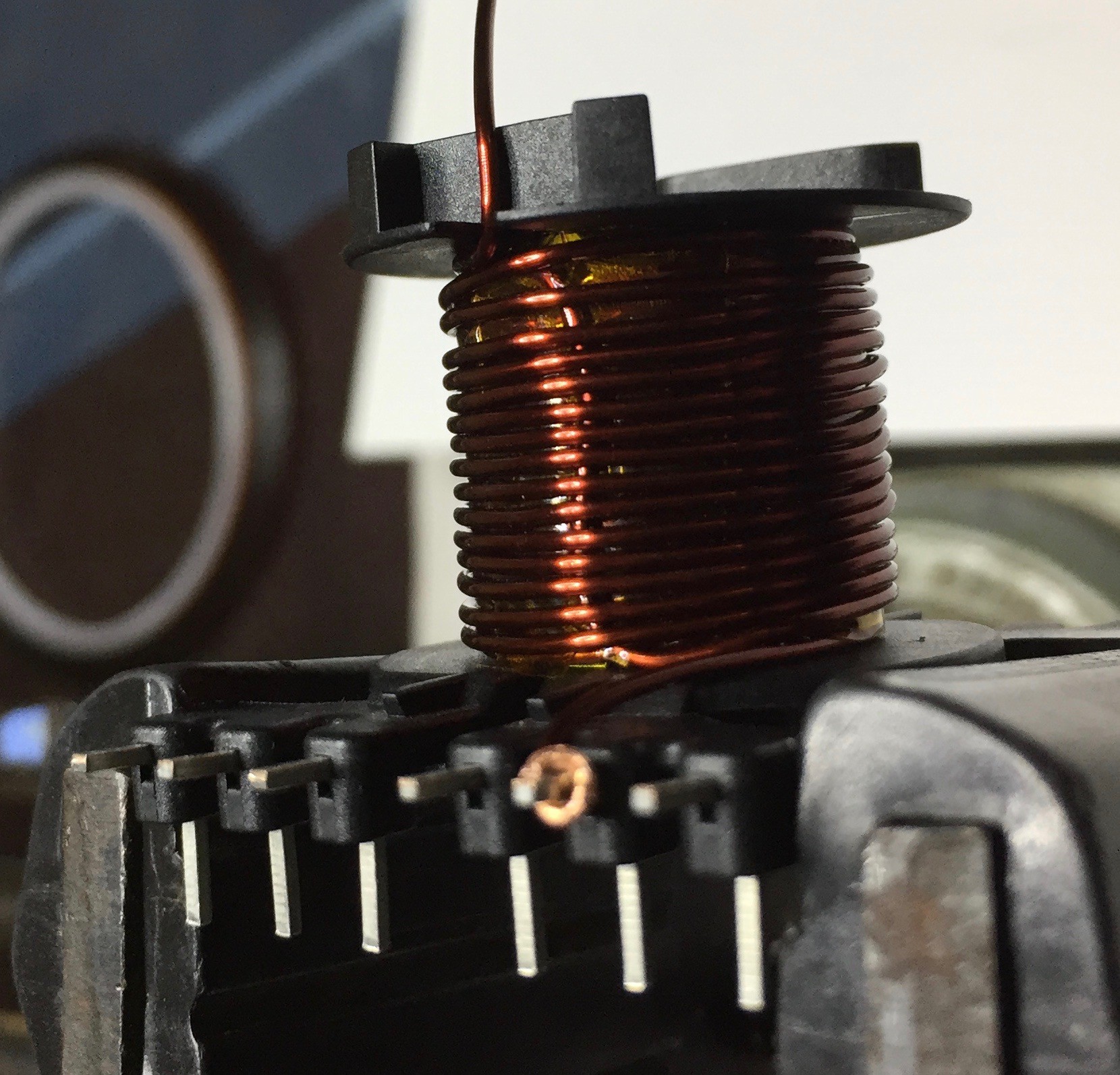
1) Wind high voltage secondary first. Two layers of 16 turns each. Terminate to pins 7 & 8. Apply one layer of tape over first layer. Begin second layer using foldback technique.
![]()
Above: 1st layer complete with tape.
![]()
Foldback taped in position and ready to wind second layer.
![]()
Second layer complete.
2) Apply one layer of tape to completed secondary. Leave unterminated (stuff into bobbin center) until complete with other windings.
![]()
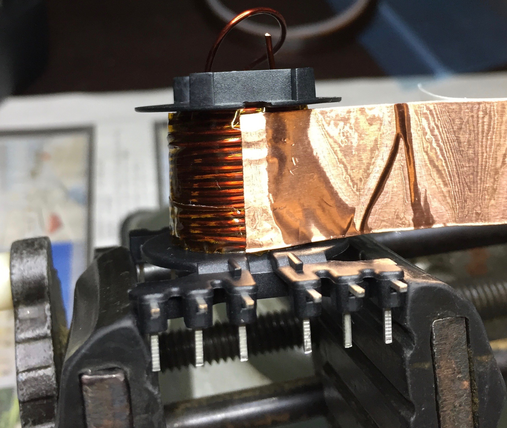
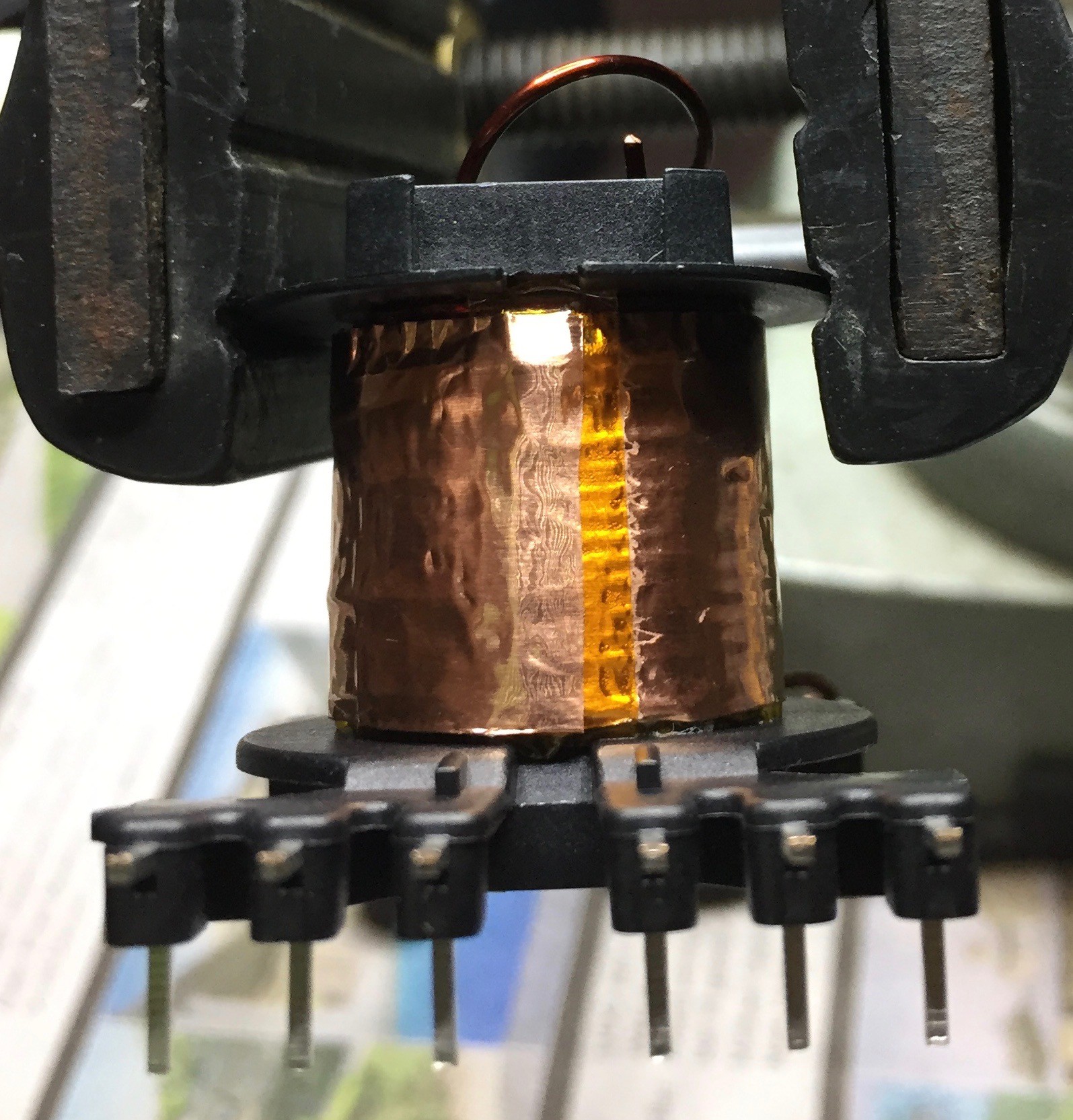
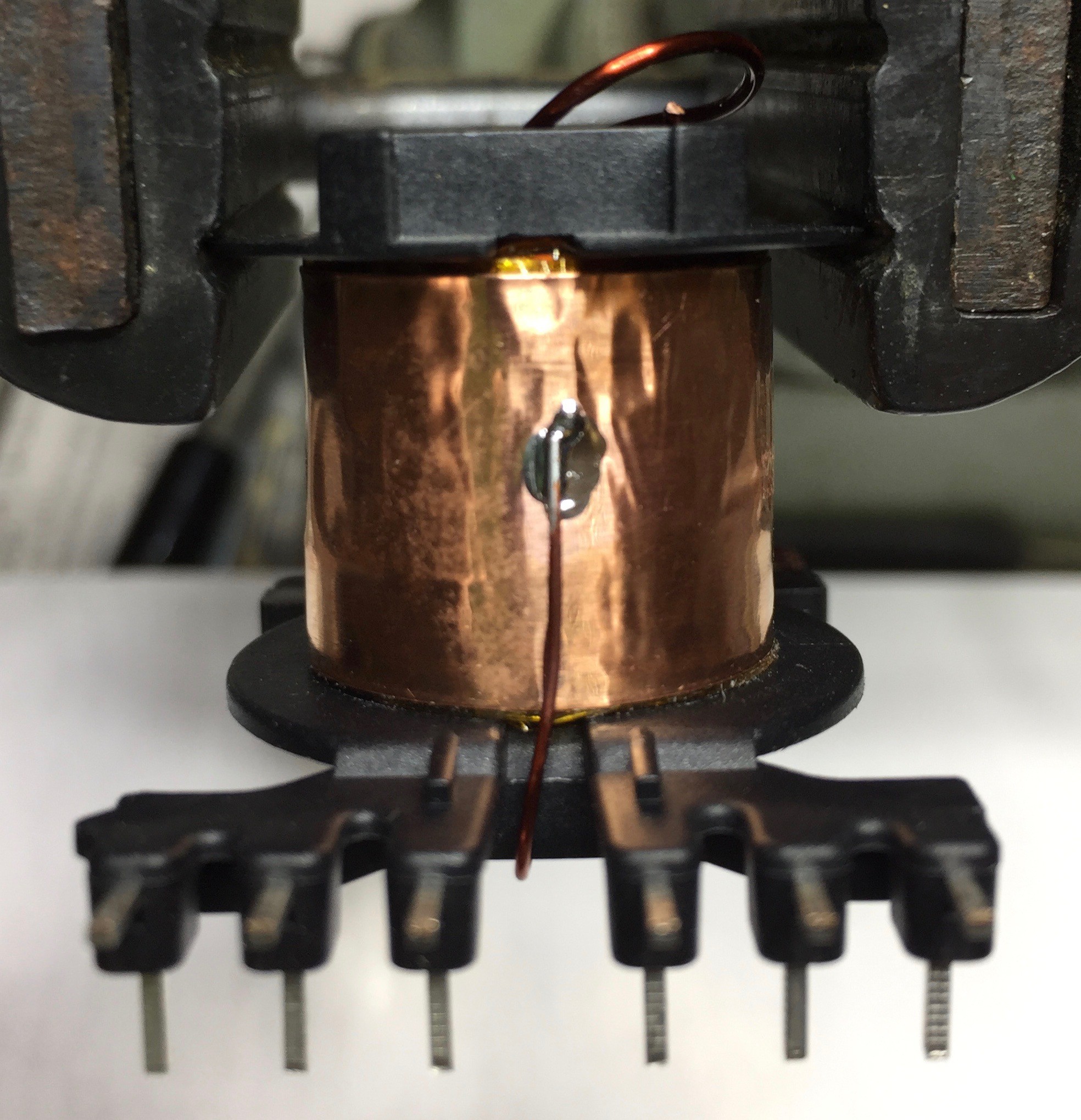
3) Install Faraday screen (terminates to secondary (-)). The copper tape should be trimmed to a width of 17mm. Measure a length that allows for a few mm of overlap. The ground lead will connect to pin 12 on the bobbin so the turn should start on the opposite side of the bobbin.![]()
4) Before completing the turn apply tape over the start of the turn to avoid a short. Then complete the turn.
![]()
![]()
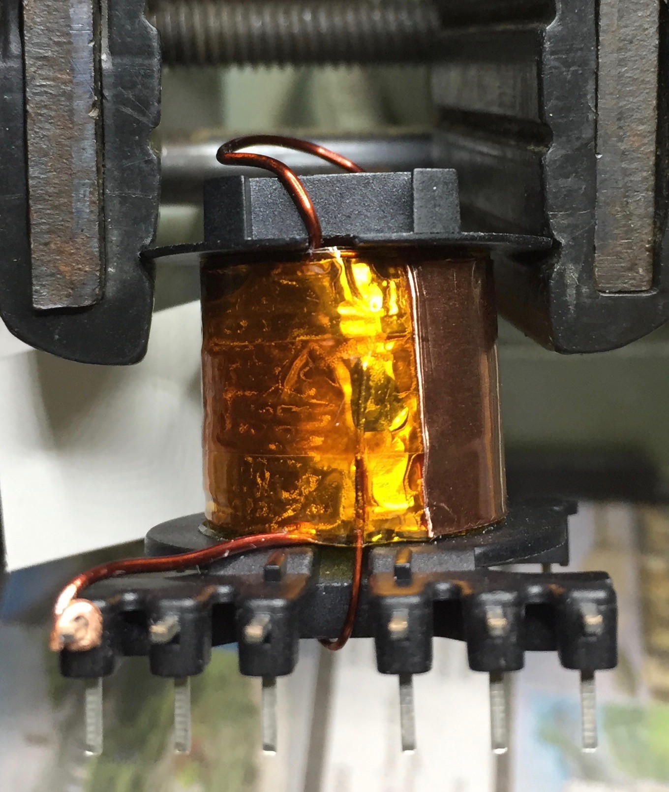
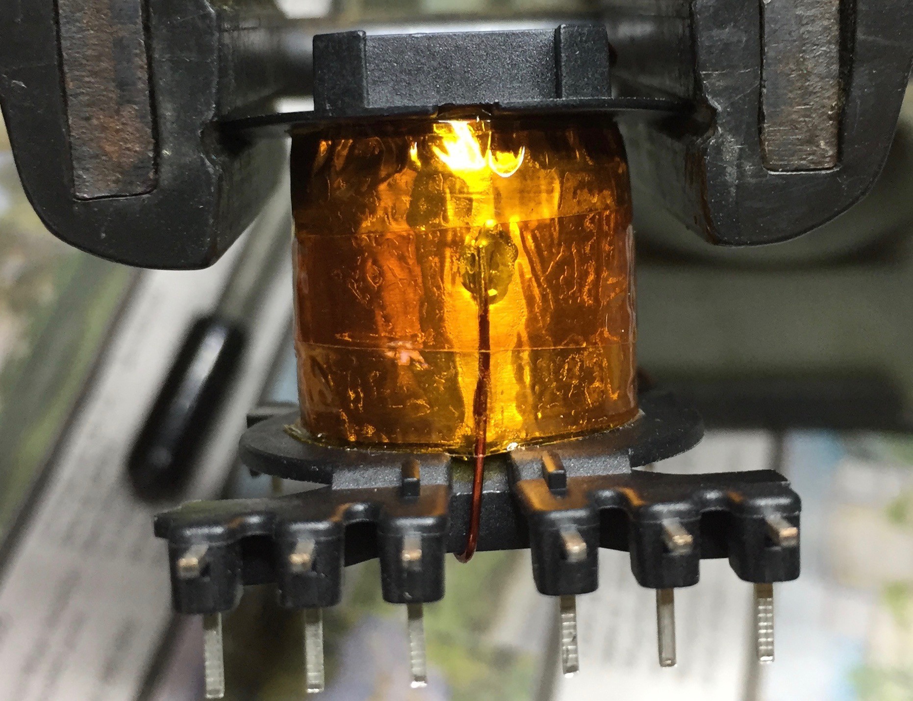
5) Opposite the termination (other side of bobbin) solder a ground lead (24 AWG magnet wire) to the center of the screen and terminate to pin 12. Then apply a layer of tape: be sure to overlap the edges of the bobbin so the next screen doesn't short to it.![]()
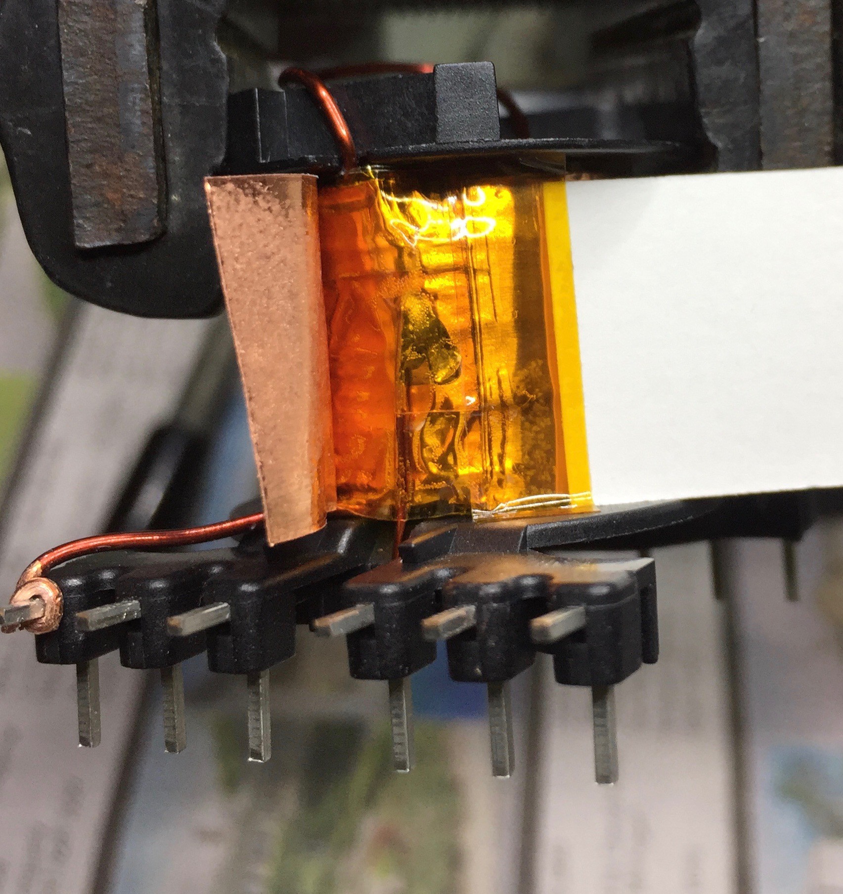
6) Install the second screen. This one will terminate to the primary (-) so the turn should begin on the secondary side. There is no pin available to connect the ground lead (it terminates to PCB when installed) so protect the lead by stuffing in bobbin when done. Otherwise the build is same as first one.Pictures:
![]()
![]()
![]()
![]()
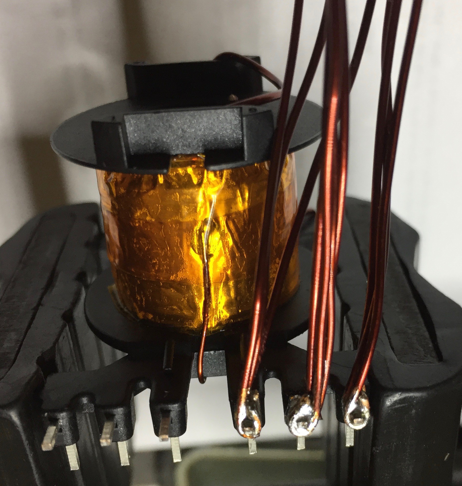
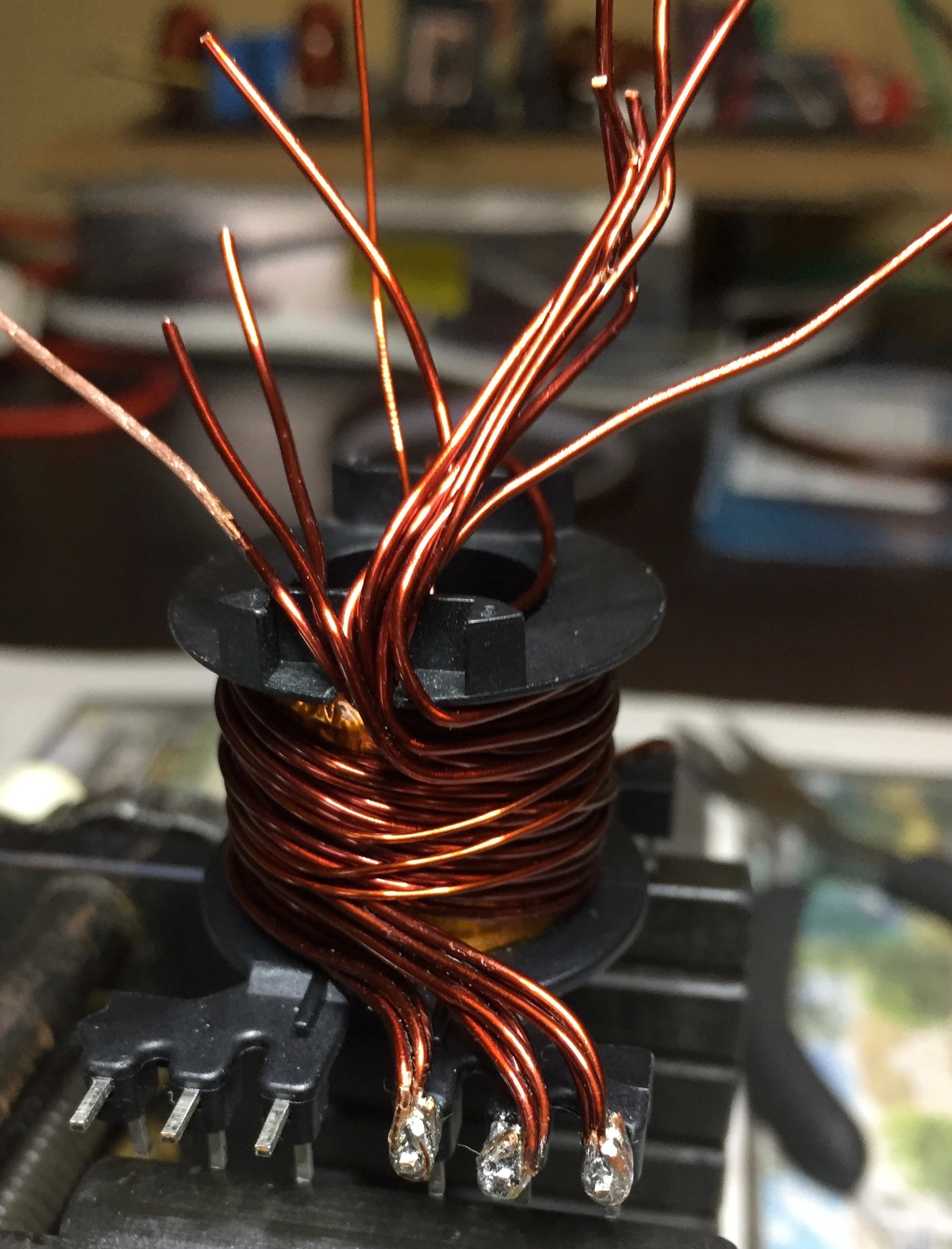
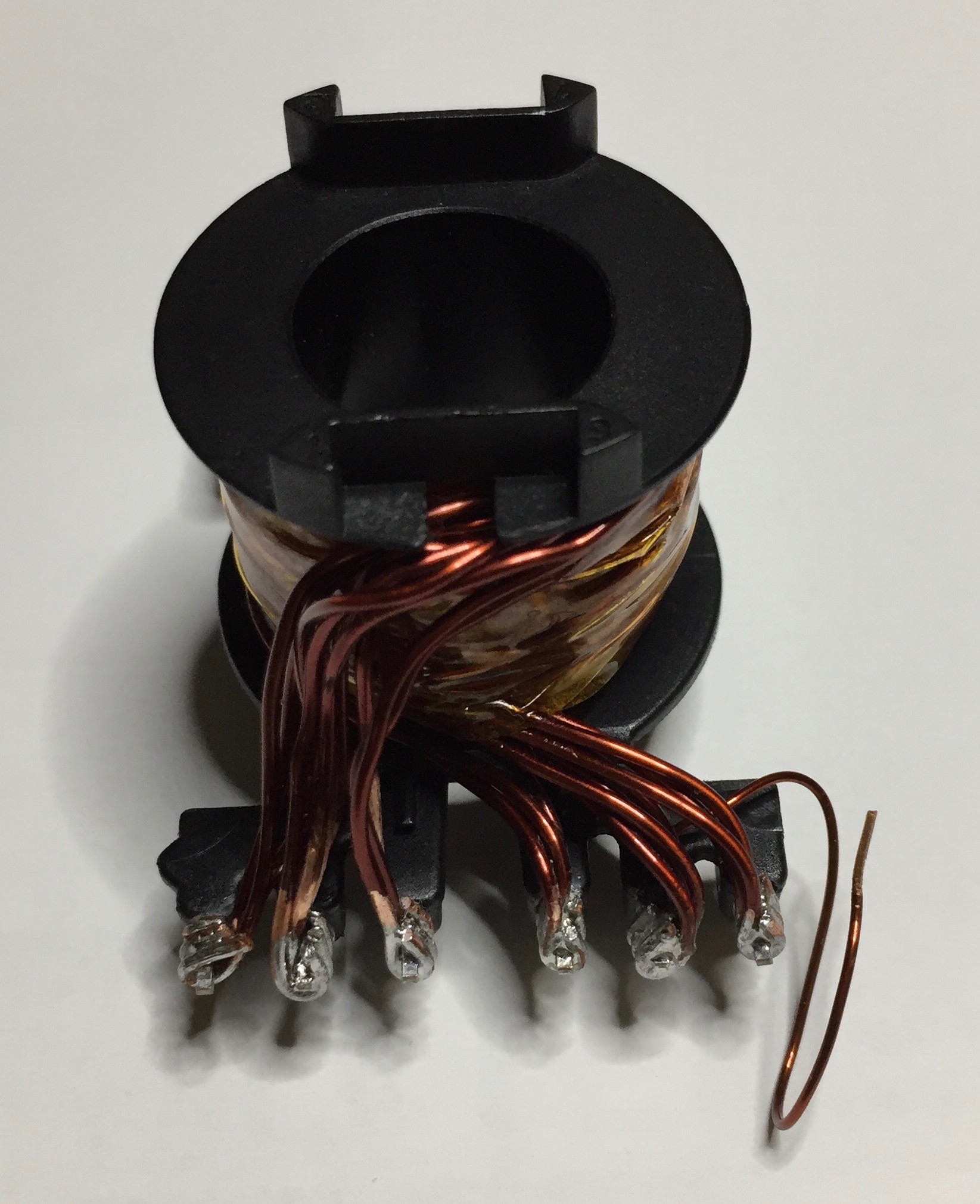
7) Winding the primary is difficult because it consists of ten individual strands of 20 AWG terminated to sets of pins. Pins 1-3 are for one end of the winding and 4-6 the other. Start by measuring ten strands to allow for two turns (with extra). Terminate 3 leads respectively to pins 1-3. One pin will need to accommodate four.
![]()
8) Wind two turns. Keep the strands in each turn as parallel as possible and cover as much of the bobbin as possible (important to minimize leakage inductance).![]()
9) Terminate the strands to pins 4-6.10) Then wind the three turn, 24 AWG auxiliary secondary on top of the primary. No tape is necessary and placement of turns is not critical. Terminate to pins 10 & 11.
Then apply a few layers of tape to secure & protect the windings.
![]()
![]()
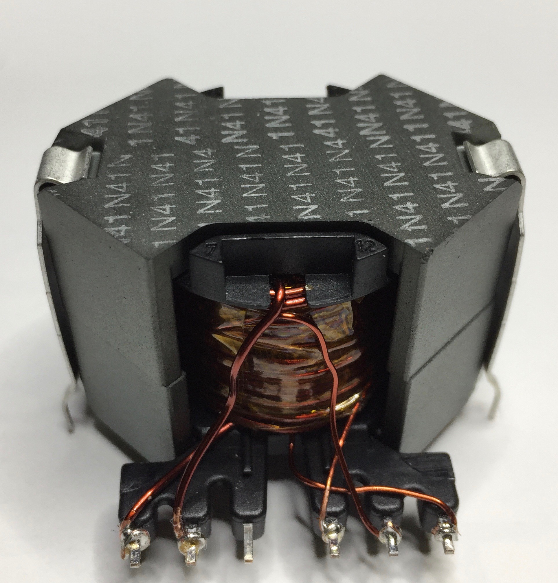
11) Install the core and protect the primary faraday screen lead until ready for installation.![]()
12) Use a DVM to check for shorts. No winding should be connected to another or the faraday screens.13) Functional check. It's a good idea to make sure there are no shorted turns, particularly with the screens. This also provides a static validation of proper layering and taping.
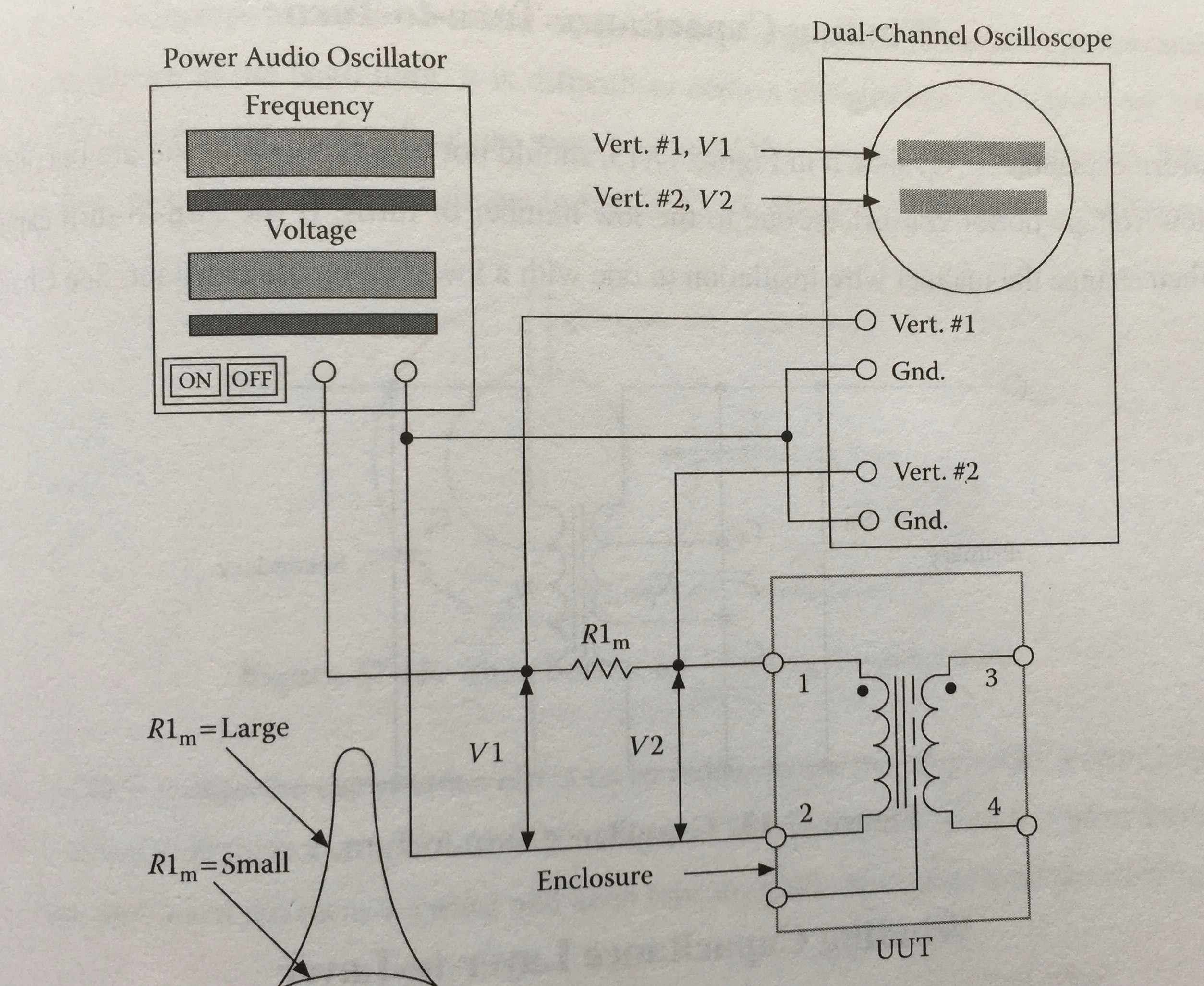
For this test you will need a 2-channel oscilloscope, function generator, and a 1/4W resistor between 3-5KΩ. Connect the primary according to this diagram (image taken from McLyman, C. (2011). Transformer and Inductor Design Handbook (4th ed) New York CRC Press, pp 17-9.):
![]()
Leave the secondaries and screens open. Set the function generator to 50kHz generating a 4V P-P sine wave.
Sweep thru 400kHz. As 400kHz is approached the amplitude will increase and the phase will align with channel 1. Amplitude should peak within 10kHz of 400kHz. This is the transformer's resonant frequency and is defined by winding inductance and parasitic (lumped) capacitances.
IF you get no signal on channel 2 it means there's a shorted turn. The transformer will not work at all since the flux is shorted as well (it also means you'd have a dead short across the bridge).
If the resonant frequency is substantially different (esp. lower) it indicates a potential problem with the build.
-
2Output Inductor Build
This instruction is for building the output inductor (two required - L401, L402). It describes materials and fabrication guidance but assumes the reader has experience assembling magnetics. Additional information can be found in the magnetics zip file and the 'inductors' tab of the Excel design file.
The following materials are required:
- Magnetics High Flux toroid core, #C058547A2
- Magnetics toroid mount, #TVH38134A
- 3M 1mil Polyimide tape 1205 (various widths) or equivalent
- 22 AWG MW35C HY magnet wire
- Silicon adhesive
You will likely need to acquire the core & mount from a Magnetics Inc. distributor such as Dexter or Elna.
1) The 'inductors' tab of the Excel design workbook provides the detailed winding data. The inductor consists of 100 turns of 22 AWG magnet wire (two strands). The winding will require about 2-1/2 layers and tape can be used on each layer to secure.
2) The precision of each layer and amount of tape use isn't critical.
3) The strands of each end should be terminated to the respective posts at each end of the mount.
4) Secure the wound inductor to the mount using a dab of high temp silicon RTV or similar.
5) Functional check. Like the transformer, it's a good idea to check the resonant frequency.
Same setup: 2-channel oscilloscope, function generator, and a 1/4W resistor between 3-5KΩ. Connect according to this diagram (image taken from McLyman, C. (2011). Transformer and Inductor Design Handbook (4th ed) New York CRC Press, pp 17-9.):
![]()
Resonant frequency should be around 300kHz. If the frequency is substantially lower then there's excessive capacitance and that could cause problems. In general, higher frequencies are okay.
No channel 2 signal indicates a short.
-
3SSR Flyback Inductor
This instruction is for building the SSR flyback inductor - L201. It describes materials and fabrication guidance but assumes the reader has experience assembling magnetics. Additional information can be found in the 'ssr-flyback' tab of the Excel design file.
The following materials are required:
- TDK ferrite toroid core, N87 material, mfg #B64290P0037X087, Digikey #495-5096-ND
- 26 AWG MW35C HY magnet wire
The primary consists of 6 turns and the secondary 17. 26 AWG wire is recommended for both for durability but the secondary can use 28 or even 30 AWG.
Polarity is critical: for the flyback to function the primary & secondary polarities must be opposite.
1) Wind the primary first. N=6. Space the turns evenly to cover the entire core.
![]()
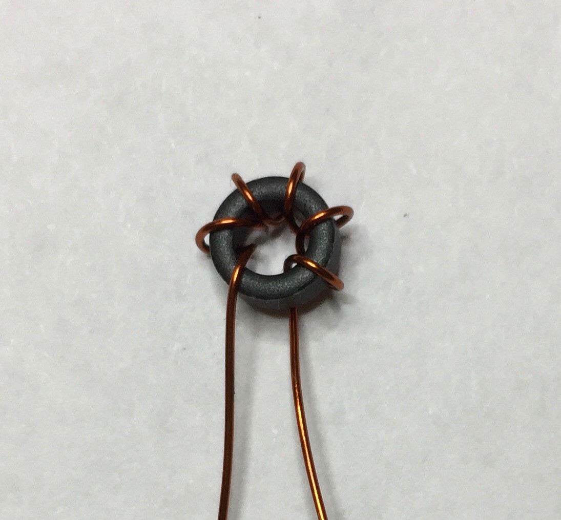
2) Wind secondary, N=17. Start the winding between where the two primary leads exit the core. Wind a half-secondary to the left & right of it (one side will have 8 turns, the other 9) so that the winding is complete with the secondary leads exiting opposite the primary.3) The inductor is wound correctly if it appears like the picture below. Note that the lead in the lower right exits the core's bottom and that in the upper right from the top. Those on the left half do the same but in reverse.
![]()
4) The function check for this one is to install it. Be sure to install with the pri & sec on the correct sides.When the controller has the SSR on you should measure 12-15V DC across the G-S of either SSR MOSFET. Make sure you're measuring across and not ground referenced.
-
4Securing the Powerpole Jacks
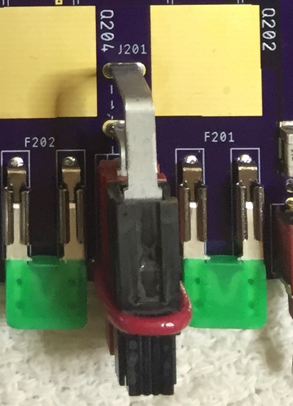
You'll notice that to each side of the PowerPole jack locations on the PCB there is a thru-hole that coincides with indents in the jacks. This is for the installation of an 18 AWG solid wire loop to secure the jacks.
This is done to provide mechanical strength & support during jack insertion.
![]()
-
5Inverter & Sine MOSFET / Heatsink Installation
This is a complicated affair, due to the use of faraday screens (EMI reduction) and installing the transistors at minimum height (reduced inductive parasitics).
You could ignore this step and install them 'normally'' but understand that you're now a test pilot (the MOSFETs still require isolation from the grounded heatsinks).
Before getting on with the install the tabs and screens must be built. You'll need the following materials:
- Squares of FR4 cut to the size of the transistor tabs with all copper removed. Total of eight for each bridge.
- Sheet of Laird K52-2, Digikey #926-1158-ND
- 3M 1/2" wide copper tape #1181, Digikey #3M1181B-ND
- 3M 1mil x 1/4" wide polyimide tape 1205 or equivalent
- Thermal paste, Digikey #CW7270-ND or equivalent
- 24 AWG solid core copper wire to connect screens to ground
- Crazyglue or equivalent
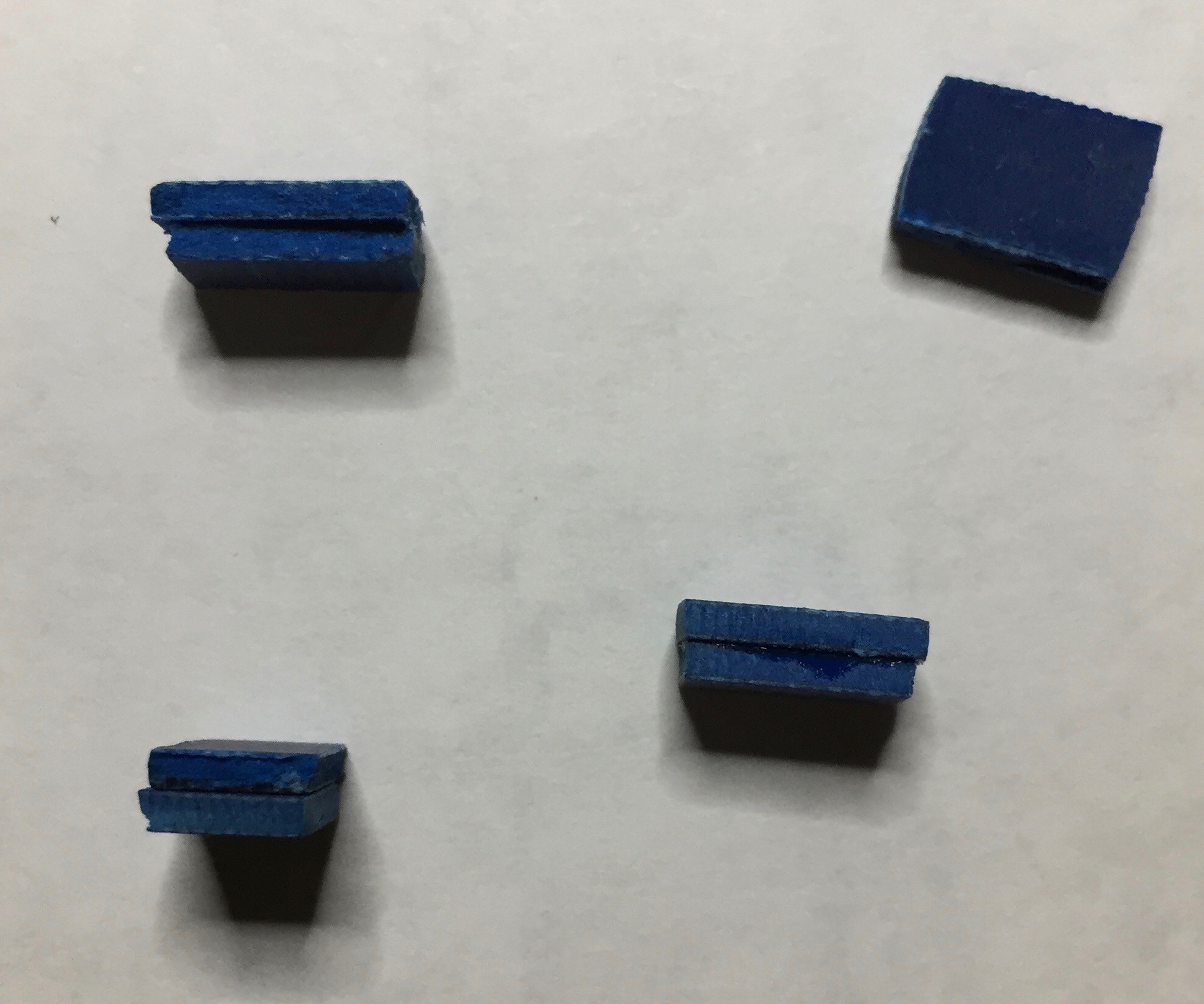
1) Fabricate cam tabs. The heatsink cams are designed to lock against the face of the transistor, but since they are mounted at minimum height it places the locking cam over the transistor tab. Two layers of 60mil FR4 placed over the transistor tab bring the height up to that of the case.
Glue two squares of FR4 together to make a set of four for each bridge.
![]()
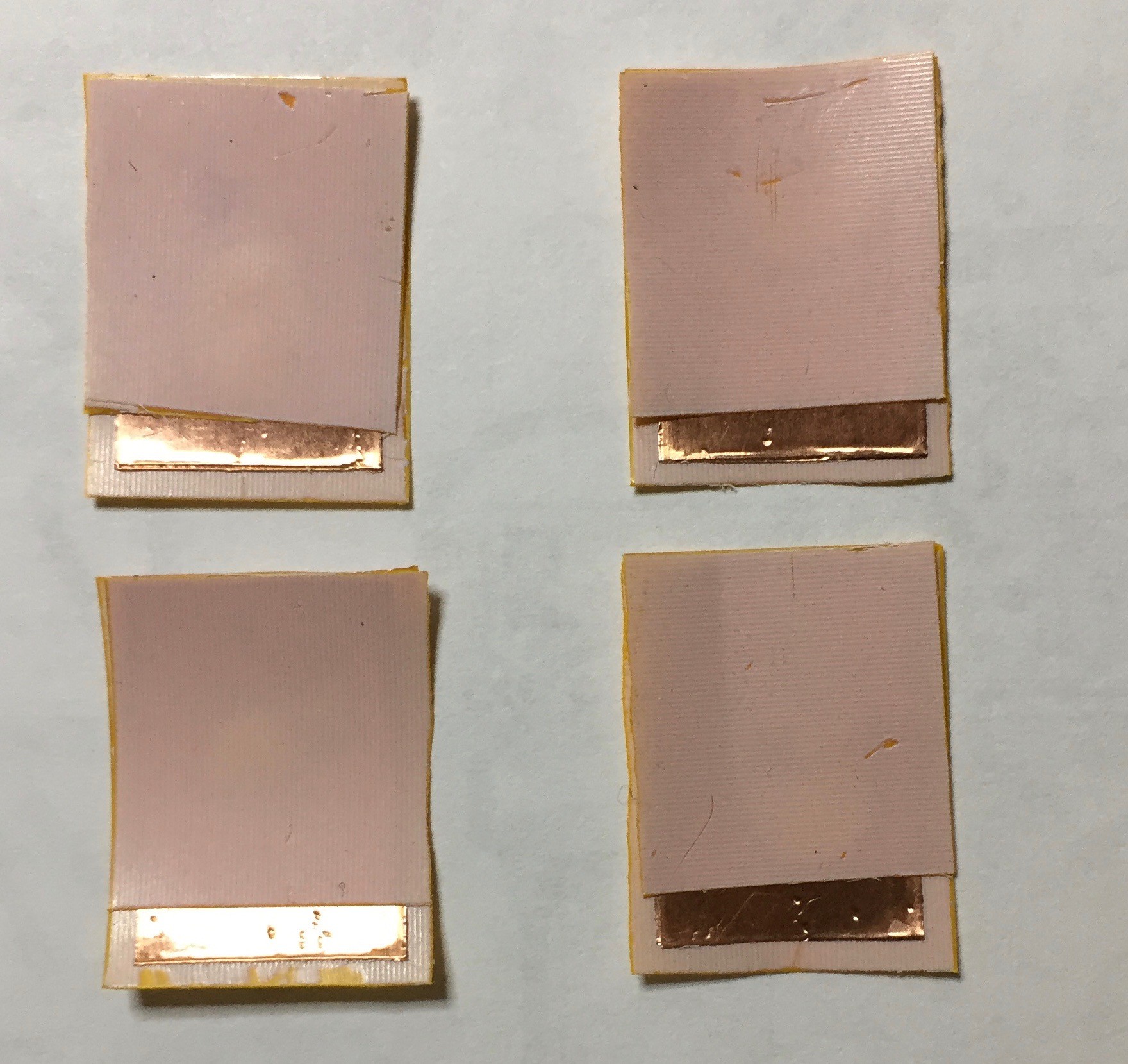
2) Fabricate insulated faraday screens. These perform three functions: EMI reduction, low theta thermal interface, electrical isolation.Each screen consists of three layers:
- Back - K52 cut to 15mm wide by 20mm long
- Middle - 1/2" wide copper, tape cut to 18mm length
- Front - K52 cut to 15mm wide by 16mm length
The K52 material is durable but should be handled with care. The white/pinkish powder-like coating is a ceramic that melts above 50C and is what provides its excellent heat transfer characteristics.
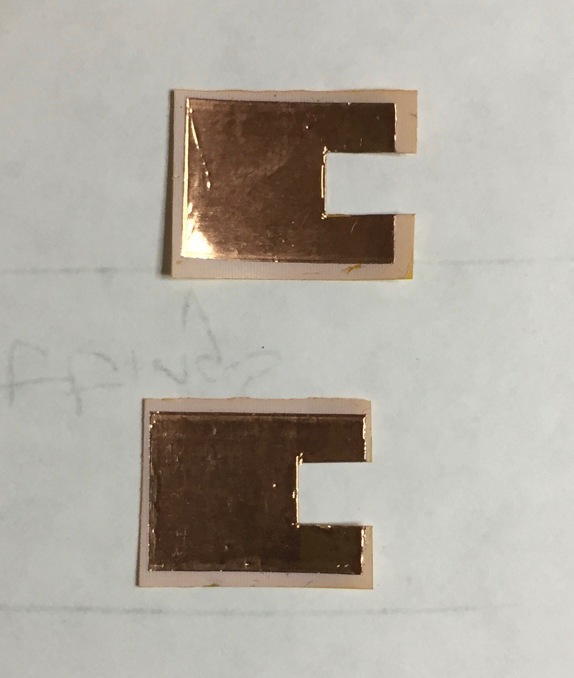
Center the copper tape top/bottom & left/right on the back. I has an adhesive backing so once set it won't shift. Position the top layer so that its top aligns with the top of the back layer. The copper layer will be exposed at the bottom. A very small dab of heatsink grease can be used to hold the top layer in position.
Assembled screens should look like this:
![]()
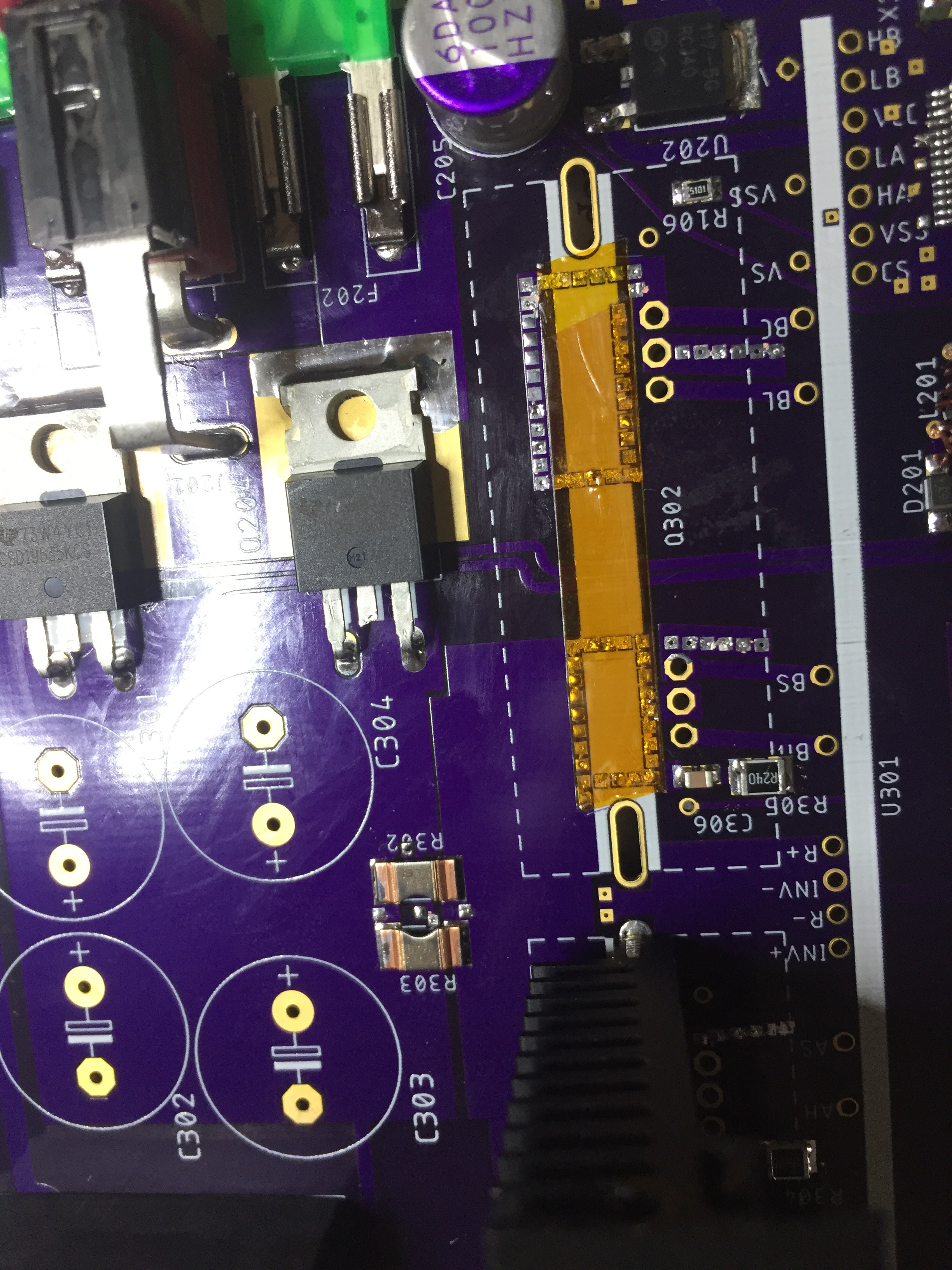
3) Place a strip of polyimide tape over the PCB white outline for the heatsink. This is to prevent the grounded sink from shorting to traces or vias.
![]()
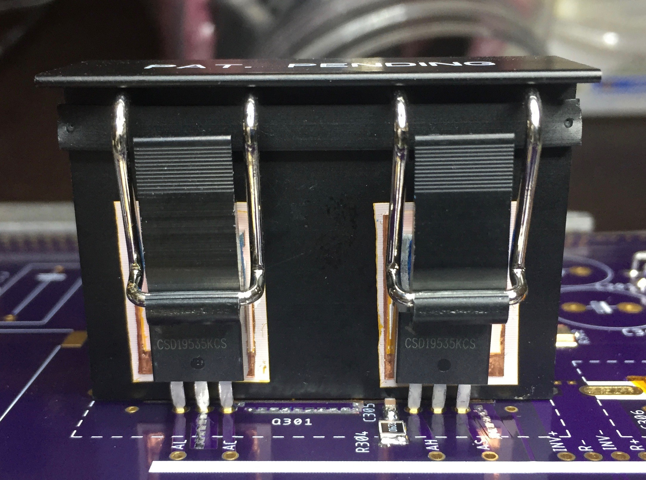
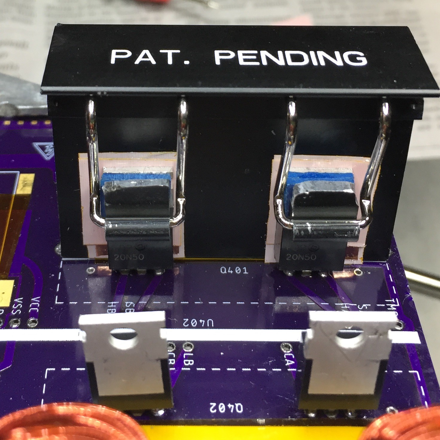
4) Install the heatsink. Position so it is flush with the board and only tack the tabs with solder at this time.5) Install the transistors. I have a genuine appreciation for the installation flexibility these heatsinks offer but they are difficult to work with. I found it easiest to first slip the transistor in, place the locking tab and lock it - without the screen. This gets the leads & case properly aligned. Then unlock & slide the screen into position and lock. Don't solder until you have both set like this:
![]()
Then solder the leads & heatsink mounting tabs.
6) Ground the screens. But first make sure the screen isn't already shorted to the heatsink. If it is it won't do its job.
There is a thru-hold adjacent to each transistor for the ground lead. 24 AWG solid copper wire is recommended. Best to first solder the board connection, then position & solder to the screen:
![]()
7) Check for shorts. Make sure the drain is not shorted to GND. -
6HV Rectifier & Heatsink Installation
Similar to but different from the bridge transistors. Screens are used here too but since the rectifiers are in plasticized cases only the back & copper layers are used.
You'll need the following materials:
- Sheet of Laird K52-2, Digikey #926-1158-ND
- 3M 1/2" wide copper tape #1181, Digikey #3M1181B-ND
- 24 AWG solid core copper wire to connect screens to ground
1) The rectifiers are mounted back-back on this sink. If you will be using a screw (as opposed to a stud) then first drill-out the mounting hole threads.
2) Cut the layers. Two sets are needed:
- Back - K52 cut to 15mm wide by 20mm long
- Middle - 1/2" wide copper, tape cut to 18mm length
Note that the top of both layers must be cut-out to accommodate the screw.
Important: make sure the copper cut-out is wide enough to avoid shorting to the screw. A short renders the screen useless.
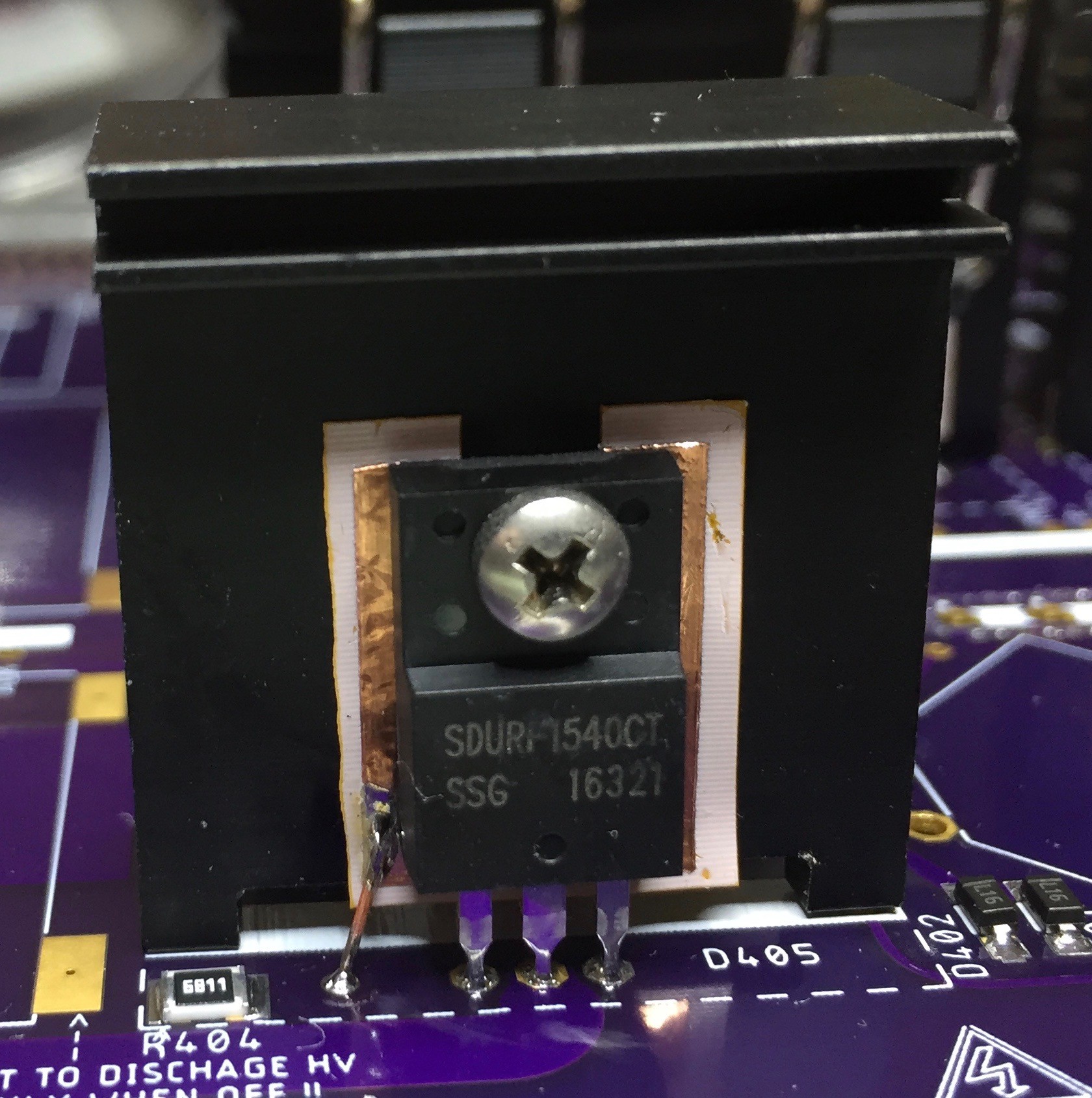
3) Assemble the layers. The copper should be centered top/bottom & left/right.
![]()
4) Install sink & rectifiers Check to make sure the screen isn't shorted to the screw or heatsink.5) Ground the screens:
![]()
6) Check for shorts to secondary GND. -
7Sine Heatsink & Controller Installation
I think I commented about my love/hate relationship with these Ohmite sinks in another post. Another drawback is that the length of the cam arm makes installation difficult when there is other stuff within its radius. This is the case for the sine bridge.
1) Both heatsinks MUST be installed before the controller card.
2) The first heatsink (doesn't matter which one) installs easily since nothing is in its way.
3) When installing the second one do not solder the heatsink posts until everything is assembled - transistors in with screens, clips locked, etc. This allows enough tolerance to lean the sink back and swing the cams locked. It may result in the transistors sitting a bit higher but not enough to be a problem.
4) Install the controller card.
5) OPTIONAL: a little machining makes this install much easier and avoids the gymnastics. I needed to do this when troubleshooting failures in the low-side MOSFETs:
![]()
The card still needs to come out but clipping in the transistors is easy.
-
8Fan Install
The fans should be installed as the last step in board assembly. They are secured by straps of wire soldered to the pads at each end. It's recommended to place a few layers of polyimide (or similar) tape under the fans to dampen vibration.
![]()
Use 24 AWG solid core copper wire for the strap.
-
9Gate Drive Cards
The design consists of a main (power) and two daughter PCBs:
- Inverter gate drive
- Sine controller & gate drive
The gate drive PCBs can be installed as last steps in assembly or you may choose to install them as you complete each section. It's not a bad idea to test the inverter section before moving on to the sine.
The daughter boards mount to the main with conventional 100mil right angle pins and they provide good mechanical support. Board vertical alignment is assured by the use of pin sets on both sides.
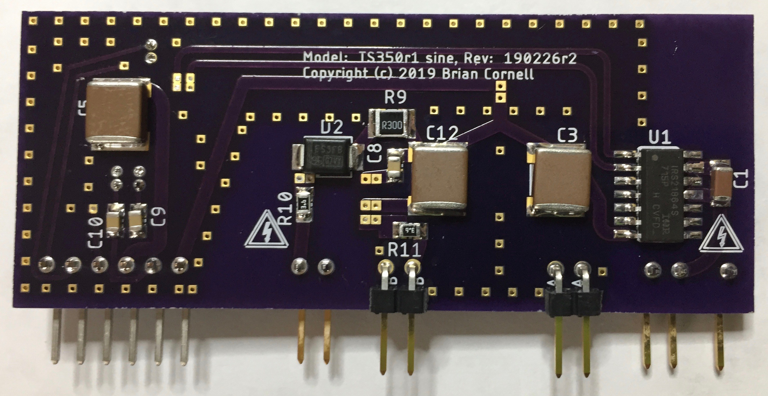
Be sure to mount pin sets to the correct sides. Below are pictures of both cards.
Inverter gate drive front:
![]()
Inverter gate drive back:
![]()
Sine controller front:
![]()
Note that the side board has three jumpers positioned around the PIC. These are for updating the firmware. The fit with the 30mm fan is tight and just barley gets around the lower right jumper. If you're not worried about updating the firmware you could omit the sockets and solder jumpers in place.
Sine controller back:
![]()
-
10Current Sense Circuit Modification
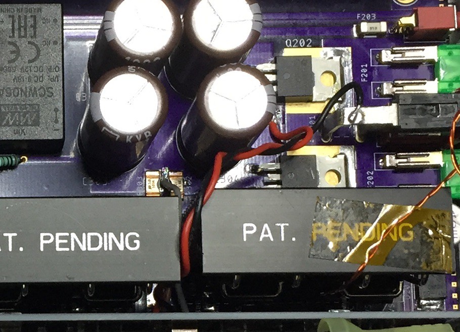
There's a design problem with the current sense circuit layout in board rev 190404. It will be described more fully in a log post. In short, the signal from the 'B' side of the bridge is suppressed for the first ~ 1/3 of the on-time due to the circulating current in the bridge. This is due to the trace layout.
This instruction provides a work around that improves the signal adequately for the unit to function without problems. The fix is to avoid the PCB traces and instead use discrete wires to connect to the sense resistors and power supply.
1) Use 24 AWG stranded connection wire.
2) Use the vias at each end of the sense resistors to connect to R+ & R-.
3) Connect the positive supply lead to the (+) copper pour between the SSR MOSFETs. You will need to remove some of the solder resist.
4) Connect the negative supply lead to the (-) PowerPole lead.
Picture of modification:
![]()







Discussions
Become a Hackaday.io Member
Create an account to leave a comment. Already have an account? Log In.