Homebrew Machine 2
An 8 bit breadboard computer based on the Malvino SAP-2.
An 8 bit breadboard computer based on the Malvino SAP-2.
To make the experience fit your profile, pick a username and tell us what interests you.
We found and based on your interests.
I've mostly finished my Arduino sketch for generating the instruction words that will drive the control logic in the computer.
We define a bank as an EEPROM with 8 output lines. With that in mind, we can define as many control lines as we want to support:
We can define an instruction as a pair of flags (defining addressing modes or that we want to write memory) with a set of operations per time step:
Since we only define the value of control lines for the bank we're writing, we can fold an arbitrary number of control lines into the single byte that represents this EEPROM's output lines. This lets the stepwise definition of each instruction be very readable inline. I liked this approach better than the giant table I was using before.
Addressing modes are drawn from the 6502, which I want to learn to implement in more detail:
There are still more modes to support.
The Emit function will output the byte stream that implements the instruction for each addressing mode. The opcode is the address of the first timestep of that instruction for a given addressing mode.
Each addressing mode outputs a series of required steps to get the correct address. Not saying the above code is correct. It hasn't been tested yet (this sketch wasn't developed using a unit test rig).
Some straightforward write logic drives the hardware:
These EEPROMs use a method of writing back the inverse of data bit 7 to indicate a completed write. This particular EEPROM also cycles data bit 6 while a write is active.
The end result is, for every EEPROM, a set of steps at an address that is the opcode + timestep.
I also write the HALT step to every position on the EEPROM as a clear value. This will stop execution of the computer if we ever try to use an unimplemented instruction or some unwritten word in the EEPROM.
Here is an example with LDA imm (load register A, immediate), which is opcode 0x18:
             t0    t1    t2    t3    t4    t5    t6    t7
BankA: 18:   30    20    10    80    80    80    80    80
BankB: 18:   80     0    80     0     0     0     0     0
BankC: 18:    0     0     1     0     0     0     0     0
BankD: 18:   80     0     0     0     0     0     0     0
In this case, t0 sets bits on banks A, B, and D as the first step of an immediate mode instruction (advance the PC to get the argument). At t1 bits are set on banks A and D which transfers the value of the argument in memory to the A register. At t2 we fetch the next instruction. The rest of the timestamps (t3 ... t7) are invalid and will drive the HALT line (0x80) on bank A if accessed.
With this framework in place I just have to wire up the control lines, author the remaining instructions and memory addressing modes, and burn the EEPROMs.
Several instructions outstanding require new hardware components. I need a processor status register (for carry, zero, etc) and I'd like to add a shift register.
My old ROM burner was for very small ROMs and only had 8 address lines. Here is the new burner using 12 address lines:
Nothing special about this project. An Arduino Nano is used to serially shift bits into a chain of 74HC194 4-bit bidirectional universal shift registers. These setup the address for the inserted ROM. The Arduino manages the write enable and output enable state of the ROM. Write detection is handled by polling for a completed bit signal on the ROM itself. The ROM is an AT28C64B 8Kx8 parallel EEPROM with page write. I haven't tried the page write feature yet, but if write times get to be an annoyance I could always hook it up.
The various control lines are specified in my burner sketch as an array of logical combinations at each time step:
I need to add some circuitry to early out of the time step count, maybe with a new control line that signals the end of an instruction.
I haven't tested any of the instructions pasted above so they might be completely wrong. Just some content in place to test the burner. Now I'm ready to author a few instructions, hook up the con lines, and get on with some more advanced computing!
Been a while since an update. Vacation took me away from the home for a bit, but I have been working on finishing a few modules.
For RAM, I decided to create a control line that would select between RAM being setup by the address register or the program counter. This provides for addressing modes that want to lookup a 16 bit address at PC+1 and PC+2. I could have used some kind of internal register for this, but the RAM mux seemed like a more direct approach and I think covers all of my instruction architecture needs.
I accidentally ordered 512kx8 OTP EPROMs instead of the RAM chips I wanted, so right now I'm only running an 8k RAM. I have enough address lines for a 64k RAM, which should arrive this week. I couldn't actually find a 64k RAM chip on digikey, so I ordered 128k RAMS. Maybe I can add a bank line later.
The RAM tests out and reads and writes, address lines work correctly:
I ended up placing the PC above the RAM and the AD below. The 8K RAM label is on top of the RAM chip and to the left of it are 4 quad mux chips which select between PC and AD.
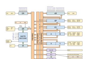
Once that was done I added the instruction register (IR) and a line of EEPROMs that will form the instruction decode logic. Instructions will be decoded by combinatorial lookup instead of microcode. Each EEPROM has 8 output lines giving me 32 control lines (for now).
I created a homemade EEPROM burner which I'll use to program each EEPROM.
Instruction bits are [ 8 bits ] [ 4 bits ] where the 8 bits are the OP code and the 4 bits are time step, so these uniquely address 256 opcodes with 16 time steps. I won't need 16 time steps, so it's possible I could use a bit on something else.
In the image above, the EEPROMs are setup to always output and never write. There's a little 4 bit counter that drives the time step.
And here is the overall computer so far:
The tasks remaining:
Then write some programs to test the range of functionality.
I'll need to add a flag status register, but I figured I'd wait until I was creating those instructions. Flags should be able to bolt onto the existing design without much hassle.
If I get through that, I'll move onto the video card. Long term project path is to create a video card and an interrupt based keyboard interface.
Today I hooked up the control logic for the A and B registers. The first step was to work out the wiring schematic on paper. Each register consists of two chips a 74HC245 bidirectional bus transceiver and a 74HC574 8 bit flip-flop. I want to be able to have three states for the register:
The register has four inputs to manage:
On the A and B registers, the control logic to drive these input lines are a Lx (latch) and Ex (enable) signal. We can break this into a state table that describes what the input lines should be to satisfy the signal:
Once we have a mapping of our logic to our chip input lines, we can create a truth table to determine the logic we want to use to actually wire up the signals. In my case I didn't want to use more than 2 gates per chip. I use quad gate array chips, so 1 chip can support 2 registers. I like to write the logic out as a phrase that matches the state table above.
We combine the system clock with L to create the input clock, so that we are only clocking the flip-flop chip when we want to load something. We can also save some wires by using a nor gate to create the 574 output enable signal, since it lets us avoid having to not E.
I did all of this on paper:
I just enjoy working out the logic on paper to be absolutely sure the schematic makes sense. The above doesn't show the nor gates which I added afterwards when I realized it simplified things a bit. There are probably other simplifications that I didn't find or didn't look for. I ended up using 1 NOT, 2 NOR, 1 OR, and 1 AND gate per register.
Another aspect of this approach is that the on state for a signal is high. This just keeps it simpler in my head, instead of having to worry about remembering something like "bit X of the CON word is not-L" because I wanted to save a NOT gate.
Here is the resulting CON wiring for the A and B registers:
The CLK and is done on the breadboard below, where I moved the clock circuit. I'll probably neaten up the lines by cutting them to the same height off the board before I implement another register's CON.
And here is the logic working. I previously latched a value into the B register and then I enabled that register to drive the bus:
Another bank of of these chips will be placed below for the X and Y index registers and then each should also have enough gates free to drive the registers on the left side of the computer. The X and Y index registers will also have INC and DEC control lines.
So next up is a clean-up pass on the wiring, then wiring up all the other registers (as well as the ALU enable line) this same way.
The idiot lights really don't need to be there, but make debugging a lot quicker. I may pull them?
Preparing for running a 2E AD&D campaign took me away from this project for a few weeks, but I've managed several hours of good work lately.
I started by hooking up the 16 bit program counter using a chained series of 74HC163 synchronous presettable 4-bit binary counter, with synchronous clear. Using settable counters is important for wiring up jump instructions later and the clear helps with implementing a reset function and clean state after power-on. This module is a little messy, as I haven't consolidated the control logic yet. As a result, colored wires that perform various functions like the reset are just hard wired with various colored jumpers and the module looks more chaotic than it will after a clean-up pass.
Below that are the two memory address registers, MARL and MARH, the low and high portion of a 13-bit address bus, wired in yellow to the RAM chip. The output of the RAM chip is then wired to the flip-flop of the memory data register. All of these registers are wired to the bus in green. Green wires are used exclusively for the 8-bit data bus.
The RAM is an Alliance Memory AS6C6264-55PCN 64K Parallel SRAM, which I haven't tested out yet.
On the right side of the board I've added a X and Y register which will be used to implement 6502-style indexed addressing modes (as well as acting as extra scratch registers when needed). No control logic is hooked up to these registers yet, but they are wired to the bus.
On the bottom left side of the board the stack pointer remains to be wired to the bus and the instruction register has to be hooked up. The IR will be wired to the instruction decoder which will reside in the middle of the board with the rest of the control logic. You can also see that I've added some extra breadboard strips at the top to span the data bus lines across board halves.
The control logic is where the real cognitive effort lies, in a future post I'll enumerate the expected control lines.
I also started wiring up a clock divider board so I could drive the computer from a 14.31818 mhz crystal at speeds stepping down to 1 hz.
Today I had a large chunk of uninterrupted time to work on this project and a bunch of progress resulted.
First, I wired up a pair of 74HC181s, 4-bit arithmetic logic unit and function generators. I didn't run through an exhaustive set of tests, but I did ensure that several operations worked correctly. I'm generally confident the wiring is good. Here you can see the ALU with various control lines labeled.
I also spent some time hooking up the control logic for the A and B registers. Each of these registers has an E and L control for enable-output and load, respectively. When Ex is high, the register should export its value to the bus. When Lx is high, the register should clock in a new value at the next rising clock edge. If both are low, the register should be in a high-impedance state.
My first pass at this logic was inefficient, using a chip array for each register. This is the right half the board (yellow wiring) in the image below.
After getting this working, I sat back to think about the geometry of the computer. I didn't like the inefficient use of the chips, I didn't like how the lines ran the entire length of the board to the bus transceiver on the left, and I also wanted to change how I was doing the central data bus.
Originally, I was thinking that the data bus would run down the middle of the machine, like in the Ben Eater computer. Here's my finished version of what that kind of design looks like:
I don't like how the control bus is a crow's nest of yellow wires. So, for this computer, I think I'll try a wider design that puts the CON logic in the center of the computer.
After an hour of re-organizational wiring and listening to Conversations with Tyler, I ended up with a much cleaner set of control logic for the registers and the ALU, although I haven't relocated the S, Cn, and M leads yet:
You can see how the green data bus lines are now daisy chained along the transceivers. The clock stepping switch that I use for testing is now also located in this central area. The white clock leads are temporary. In fact, that entire CON block will probably get refactored a couple times as more pieces come into place. I haven't worked out the layout on paper and I may do that soon.
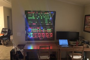
Here is a look at the complete computer so far:
The left side of the board has the program counter, the incomplete subroutine counter, and a 64K ram chip roughly where the memory will be. The center is the new CON block and the right are the registers A and B and the ALU.
I think at this point the left side needs some attention. I need to make some progress on the address bus, although I also need to complete the subroutine counter and the index register. Once all of that is done, I'll have to work on the instruction register and the instruction decoder. I figure the control logic will develop stepwise with the various modules.
I've also been thinking about input, output, and how to program the computer. I'd rather not program this machine with DIP switches. I'm leaning towards hooking up a bootstrap loader that can dump code into the RAM on startup. That would be removable, allowing me to code the computer with an assembler on the PC. For output, maybe some kind of LED array? The problem with a lot of those devices is that they require a very high refresh rate, some > 500 Mhz, which this device won't be able to deliver.
Onwards!
Yesterday I finished wiring up and debugging the 74181. The wiring of the second half is fairly disorganized, mostly because I wanted to try to fit everything on two more boards. It was also difficult to organize the logic by function, so the ICs are unlabeled. It's mostly AND gates, with a few OR, XOR, and inverters thrown in.
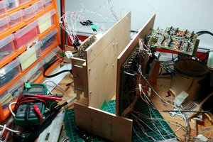
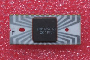
Here it is pictured next to an actual 74HC181:
Since this is a 4-bit ALU, if I wanted to use this logic in the computer project I'd need to build 2! That would make the ALU nearly as complicated as my first 8-bit computer in its entirety.
Now that I've built this model of the 74181, it'll probably go on a shelf and I'll use the actual 74HC181 IC in the computer project. I'm considering this sub-project a success and I'll assemble the ALU for the new computer next.
A quick update to note that I've wired up the generator G outputs on the model 74181. I re-organized the board a bit and co-located them with the propagation bit logic.
The board is a bit less clean now, but I think the trade-off is acceptable. Running wires to the P & G intermediate output LEDs creates a bit of a stacked bus in the middle of the board. If I didn't have those toy LEDs the overall layout would be pretty clean. It also doesn't help that b and s0 is as far away from where it's used as it can possibly be, resulting in the long white wires on the bottom of the circuit.
I've run through several test cases and everything is working, although I won't be able to show this well until I get new DIP switches. The current ones like to pop out of the board so I have to hold them down while testing.
Now I just need to add circuitry for calculating the sums and carries and then I'll have a completed ALU!
Two days ago I completed the propagator P output for the model 74181. It looked like a complete mess.
The circuit was functional, but didn't really serve the purpose of making that functionality transparent. I mean, there's a laundry list of bad things going on here.
This didn't meet my standard. I ripped everything out and reworked the circuit.
Here is the current state of the model:
The input switches are more clearly separated. These DIPS do not want to stay in the breadboard, though, so I ordered a different kind to see if I can get better results.
The organization of the logic is as follows:
I'm pretty happy with the progress so far and I've now hooked up this logic enough times that I understand it well.
The next task will be to wire up the generate bits!
I'm building a CMOS computer out of 70s technology to learn about the path we took to get from then to now, but also to develop a deep understanding of how each part of the computer works. I could read about it and it would feel like I understood the material while I was reading, but I would quickly forget. True understanding of a technology is demonstrated in the ability to use that knowledge to effect a change in the world.
I like to think of my hobbies and my work in the frame of working through a personal tech tree.
On this project, I'm applying that concept narrowly. I want to use a 74hc181 4-bit arithmetic logic unit and function generator as the ALU in my computer. I've build arithmetic units before, but not ones that also had a logic component. While looking at options for the ALU in this computer, I discovered the 74181 and it introduced me to a host of new ideas.
I knew that I could chain multiple counters or logic units together to go from 4 bits to 8 and so on and that this was done at the expense of an increasing propagation delay. The outputs of the first IC have to have stabilized for the outputs of the second IC to begin to stabilize and so forth. The more chips in the chain, the longer it takes for the final set of outputs to be stable. Clock the result too early and you get garbage bits.
The 74181 solves the propagation delay problem by using a method called carry lookahead to calculate whether an operation is likely to generate a carry. If you can do this, then you can do all your arithmetic operations simultaneously and greatly reduce the delay. I spent a bunch of time two days ago working out the boolean algebra and truth tables for P and G generations, once I heard about the idea.
The 74181 also has a clever internal implementation where it's 16 logic functions are added to the A input to create 16 arithmetic functions. This took me a while to wrap my head around. A bunch of it seems super obvious in hindsight, but the schematic and the design stumped me for quite a while.
The four S inputs select a function to apply to A and B...f(A, B). This boggled my mind when it clicked: the S inputs represent the answers to a 2-bit, 4-row truth table. S0 and S1 are inverted. So, when you set S == ( 1, 1, 0, 0 ) you are asserting "there is some boolean operation where for any A (1, 0) and any B (1, 0) the answer is 0, apply that function to my A and B". For any S you provide, you'll get back an answer that conforms to the truth table you've provided. If you set S == ( 1, 1, 0, 1 ) then you've given it the truth table for AND and it'll perform an AND on the inputs (remember the first two S are inverted). This just seems like a completely backwards way of thinking about the implementation of boolean logic and it's awesome.
Describing a function in terms of the set of its outputs, given a known and constrained range of inputs. My modern programmer brain wants to think of the options I could pick from like an enumerated menu or like some kind of library of operations. I thought of a function as a process, not as a mapping of input to output. I had lost sight of what a function IS.
The first half of the circuit above implements the carry lookahead logic and the second half implements the truth table. The Cn signal is your carry-in so you can chain ICs. The M signal selects between logic or arithmetic modes.
LET'S BUILD A 74181
I think I understand this chip pretty well, but I'd like to build an interactive model of one. Working things out on paper and pondering the ideas in the logical schematic has helped a lot, but I think wiring up each of the gates by hand will crystallize things further.
Once I have my model built, I can sub in a real 74hc181 in the new computer. The IC will be much faster, but I can feel like I've mastered the large chunk of functionality that the chip aggregates....
Read more »
Create an account to leave a comment. Already have an account? Log In.
Become a member to follow this project and never miss any updates

 zaphod
 spudfishScott
 2-Zons
 Dave Collins
Are there any schematics or detailed info available for this build