Miklos Marton
-
PCBs lessons learned
06/16/2021 at 21:53 • 0 commentsThe good:
- PCB shapes turned out to be good. The PCB was scanned then vectorised and then imported to EAGLE. This process worked out fair enough.
The bad:
- The footprint of the salvaged pushbutton is small (damn I have skipped the always verify footprints on a printout before PCB ordering) Using multiple device footprints in these cases usually a positive thing.
- Always add more info on the silkscreen if possible: having the USB coloring present would have been helpful
- When making single boards like the RJ50 side make it universal: I should have broke out all the 10 RJ50 pins to pinheaders, then it could have been repurposed for other things in the future.
- The ESD protection TVS was not at hand instead I populated NUP4302. However that part does not have connection between the in and out pins. Some extra green wiring was necessary.
The lucky:
- There were some DRC errors: the beeper pad overlapped with one connector pad.Luckily the connector pad was not connected to anywhere.
-
PCBs arrived
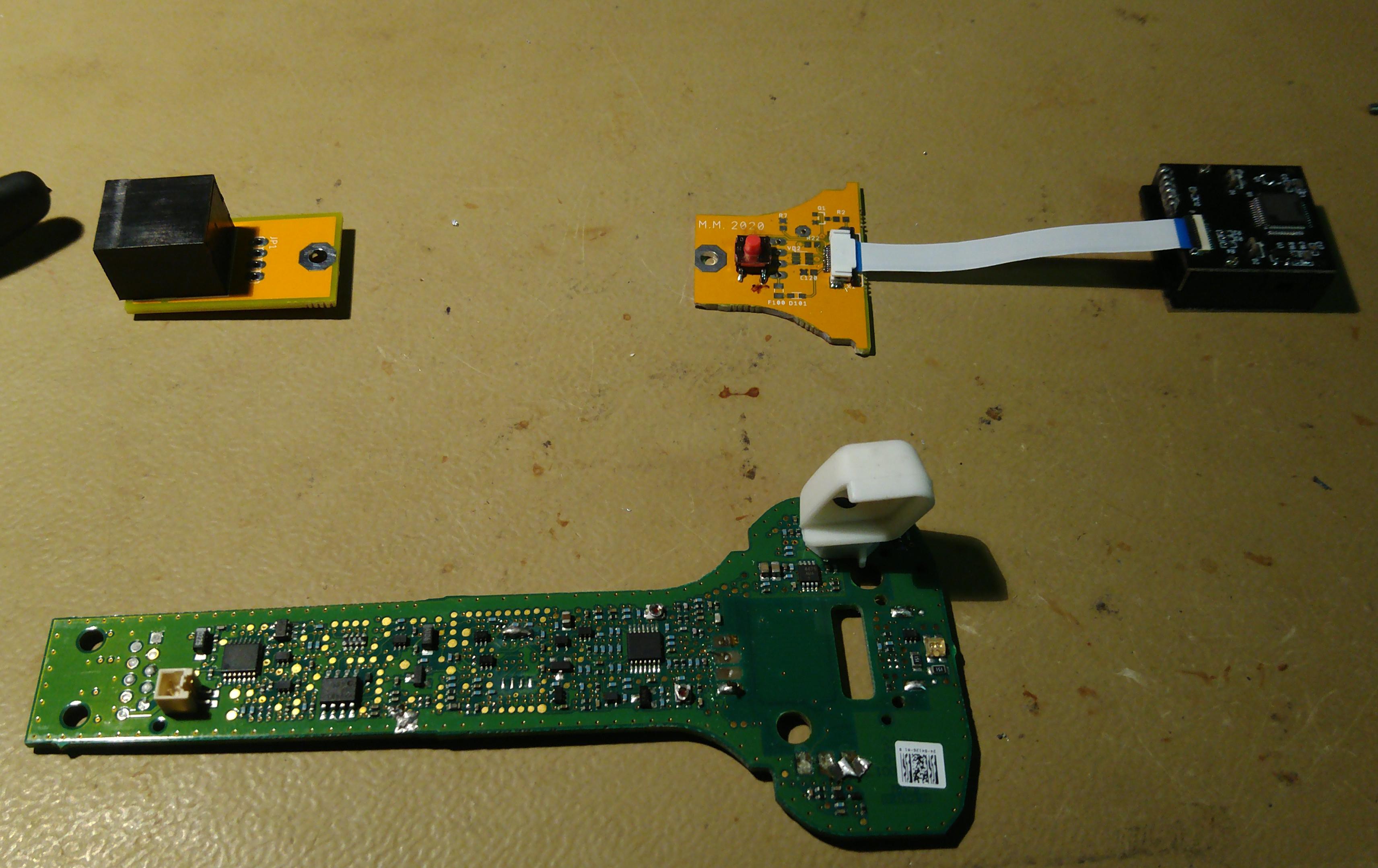
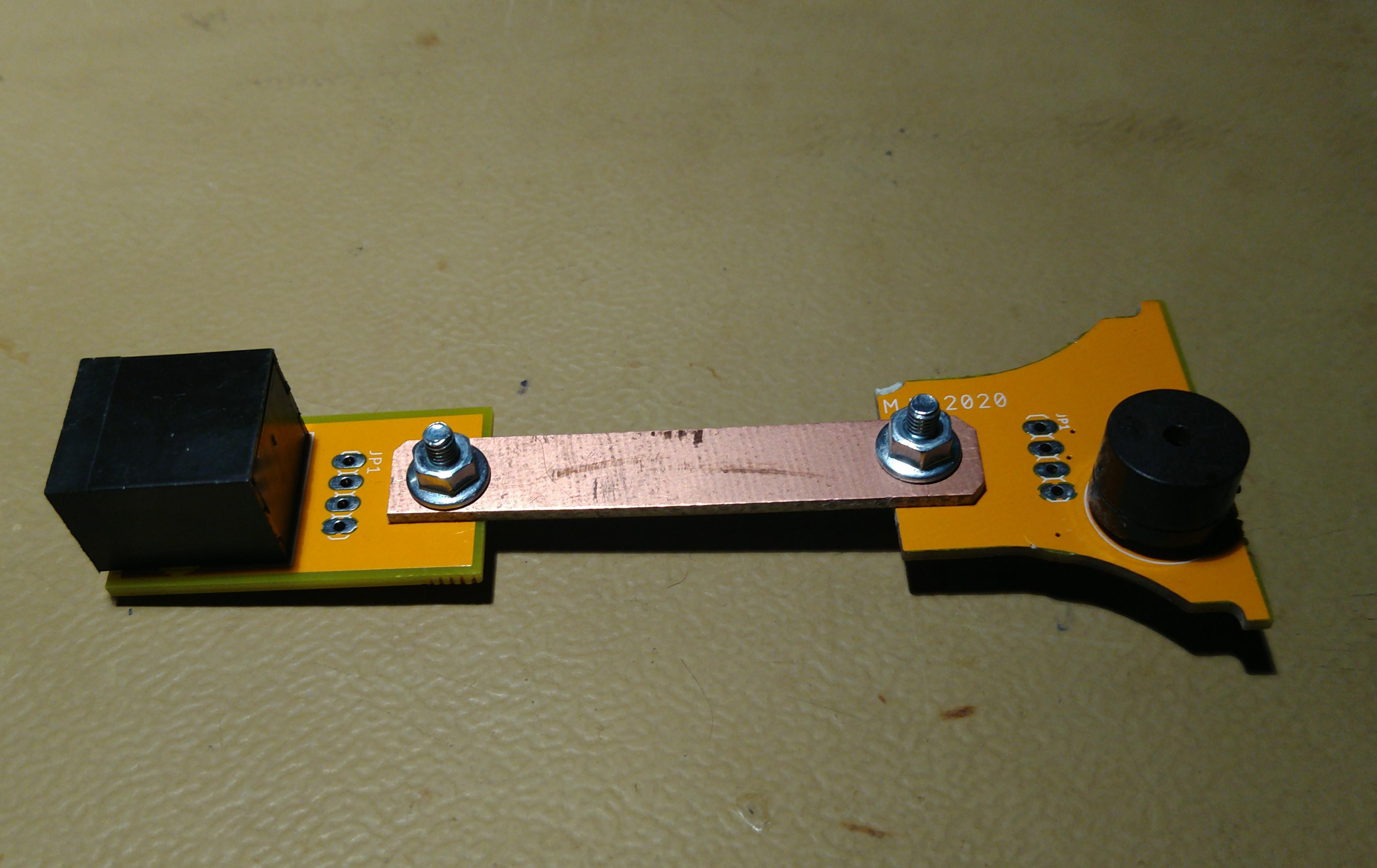
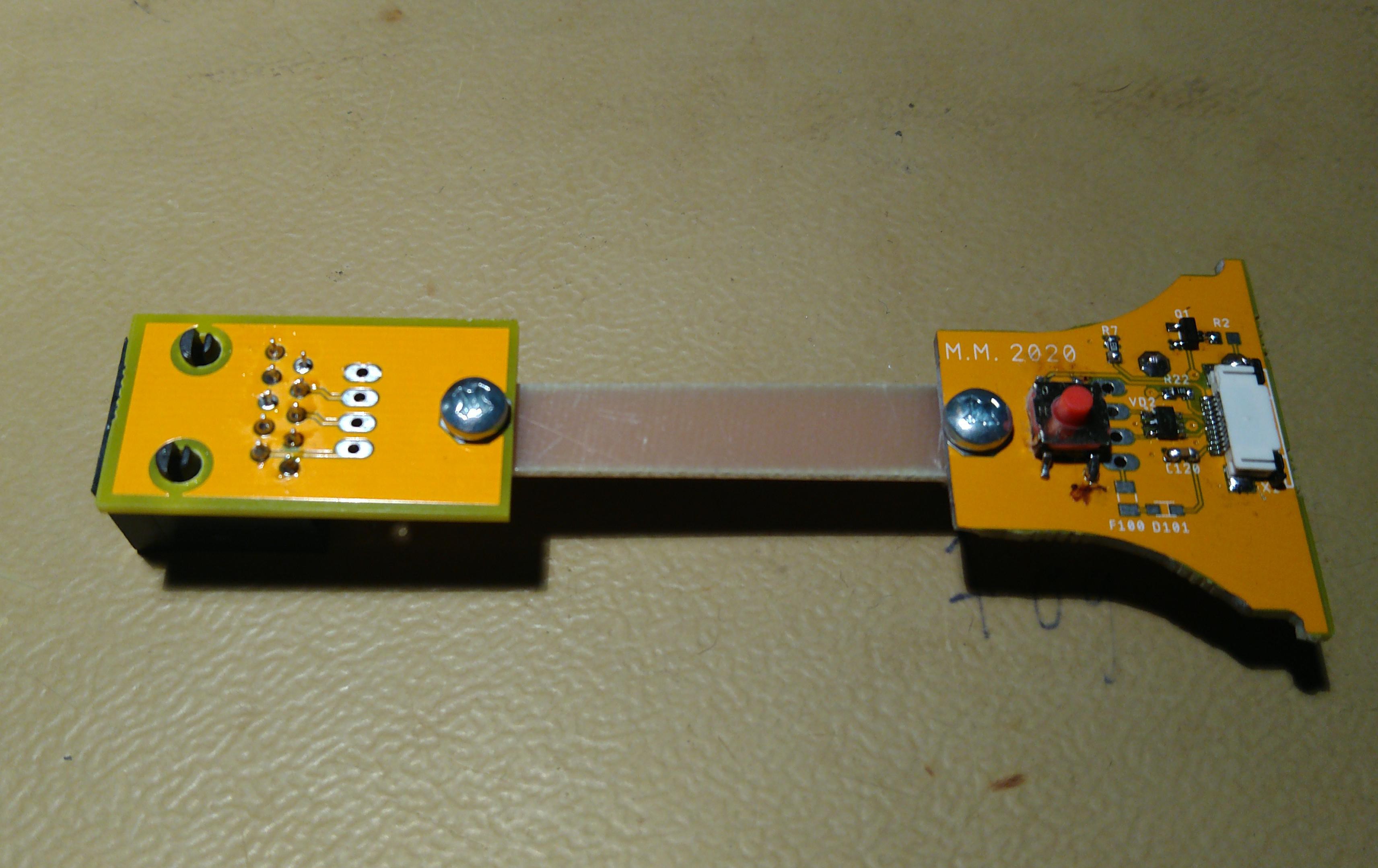
06/16/2021 at 21:41 • 0 commentsI fitted one PCB set to my last dirtyPCBs order, and received them:
![]()
As you see I made two separate PCBs to spare board space.
The RJ50 and main boards will be connected with a blank PCB strip:
![]()
![]()
Symbol LS4208 barcode reader retrofit
I have had a broken Symbol LS4208 barcode reader laying around for a while. I decided to give it a new life.