Mastro Gippo
-
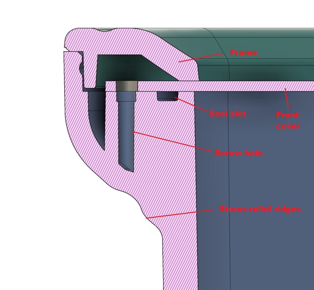
Front cover
08/30/2019 at 18:30 • 0 comments![]()
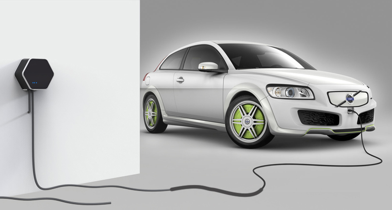
We thought a lot about the user interface for our charging station. After ditching the infinite mirror idea, we wanted something simple and elegant, inspired from the Tesla wall charger, so we started experimenting with RGB LEDs strips.
The first version of the cover for the plastic case was a laser-cut polycarbonate sheet, with a LED-strip taped to the back:
![]()
This plastic sheet can be easily UV printed for customization, but it's a bit expensive to manufacture in big quantities. I was also a bit skeptic of this solution, as that kind of plastic is not very strong, especially on the thin borders around the screws. And we know that electricians installing this would drive the screws to death, cracking the cover and resulting in expensive returns.
Turns out, as the law of the instrument states, if you only have a hammer all problems look like nails, and my hammer is electronics. And, uhmmm, what item do I daily use that is a strong, thin, semi-transparent sheet, that is also cheap, widely available, easily customizable for design and color, embeds a metal shield to better comply with emission requirements (or can be etched to become an antenna!) and can host electronics easily? You guessed it: a PCB!
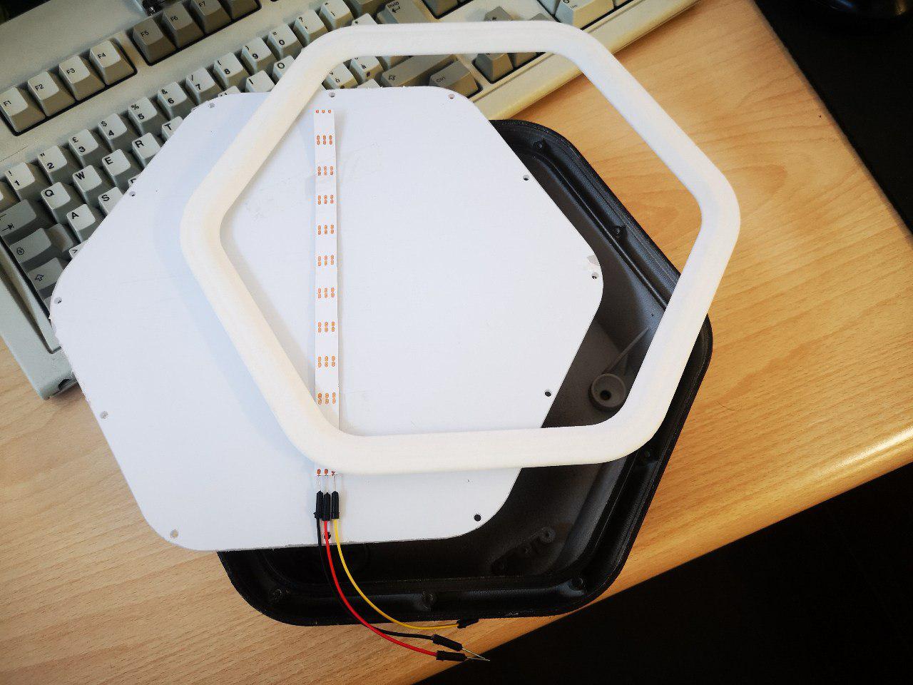
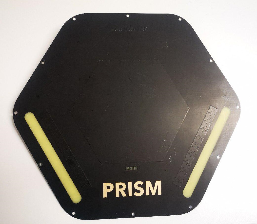
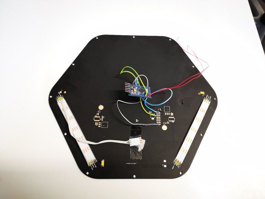
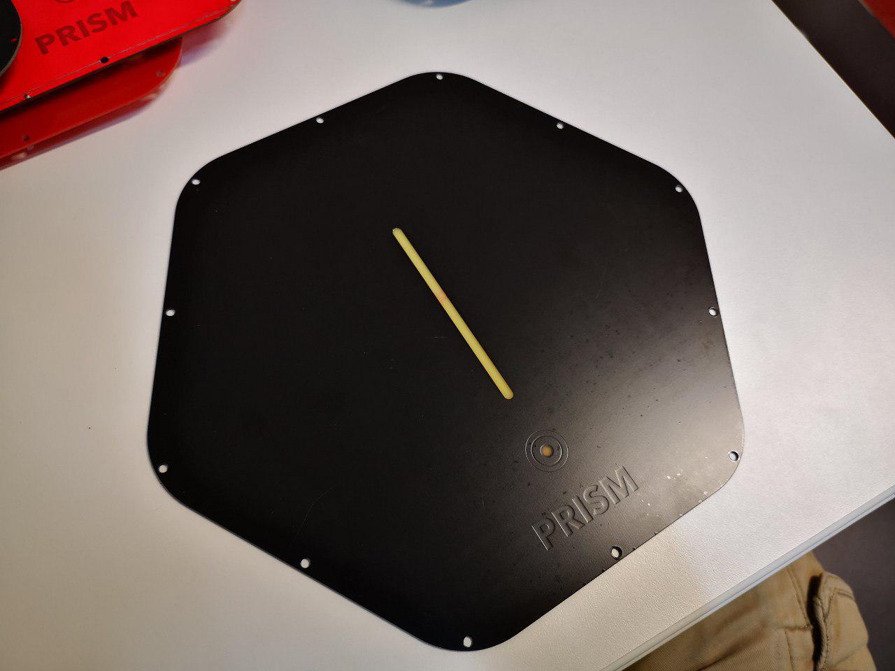
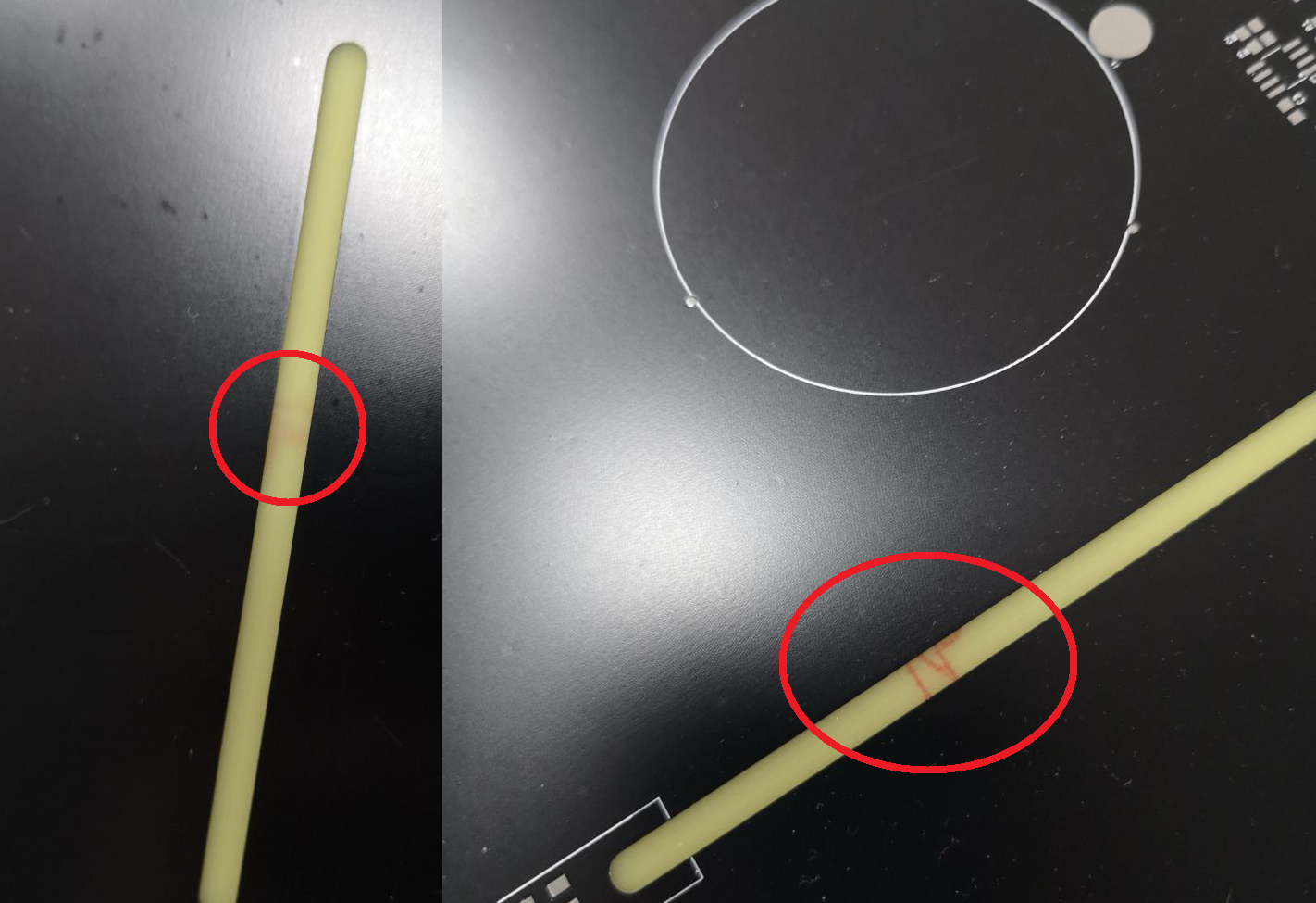
![]() This is the first prototype of that idea. The "PRISM" logo is still gold-plated copper, but with the solder mask removed. I really like the matte black/gold combination. The two slots for LED strips and the MODE button are just the bare fiberglass base, with no copper and solder mask on both sides. There's copper around the Mode button and near the LED slots for a touch button and touch sliders, controlled by a Silicon Labs CPT112S chip.
This is the first prototype of that idea. The "PRISM" logo is still gold-plated copper, but with the solder mask removed. I really like the matte black/gold combination. The two slots for LED strips and the MODE button are just the bare fiberglass base, with no copper and solder mask on both sides. There's copper around the Mode button and near the LED slots for a touch button and touch sliders, controlled by a Silicon Labs CPT112S chip.On the back, we have space for a connector to drive the LEDs and the I2C touch sensors. Here I connected it to an Arduino to test the look and feel of this solution:
![]()
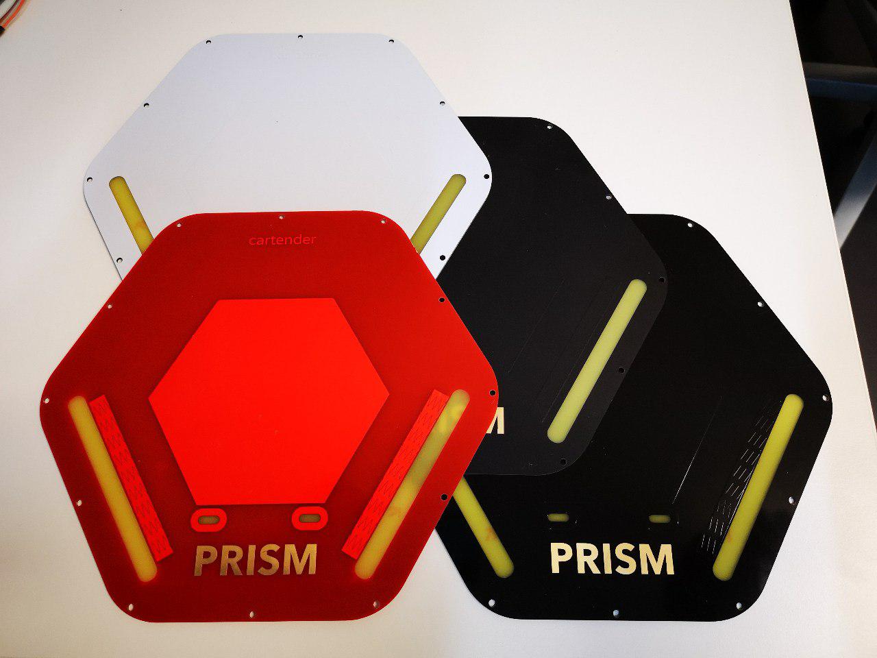
I soon prepared another revision, adding another Mode button (but without the text) and testing a bunch of different colors. The red soldermask is looking really nice as it brightly shows the copper layer underneath!
![]() Here's the back side and a video demo:
Here's the back side and a video demo:![]()
With the basic principles defined, we decided to improve the design by ditching the touch sliders and simplifying the lines:
![]()
![]()
With no need for complex Touch ICs, I simply switched to a cheap CAP1203. Having three separate inputs, I connected the central copper areas of the "P" and "R" letters in PRISM to the spare touch input pins; the idea was to use a combination of the main and the "R" buttons to reset the device and/or to trigger easter eggs.
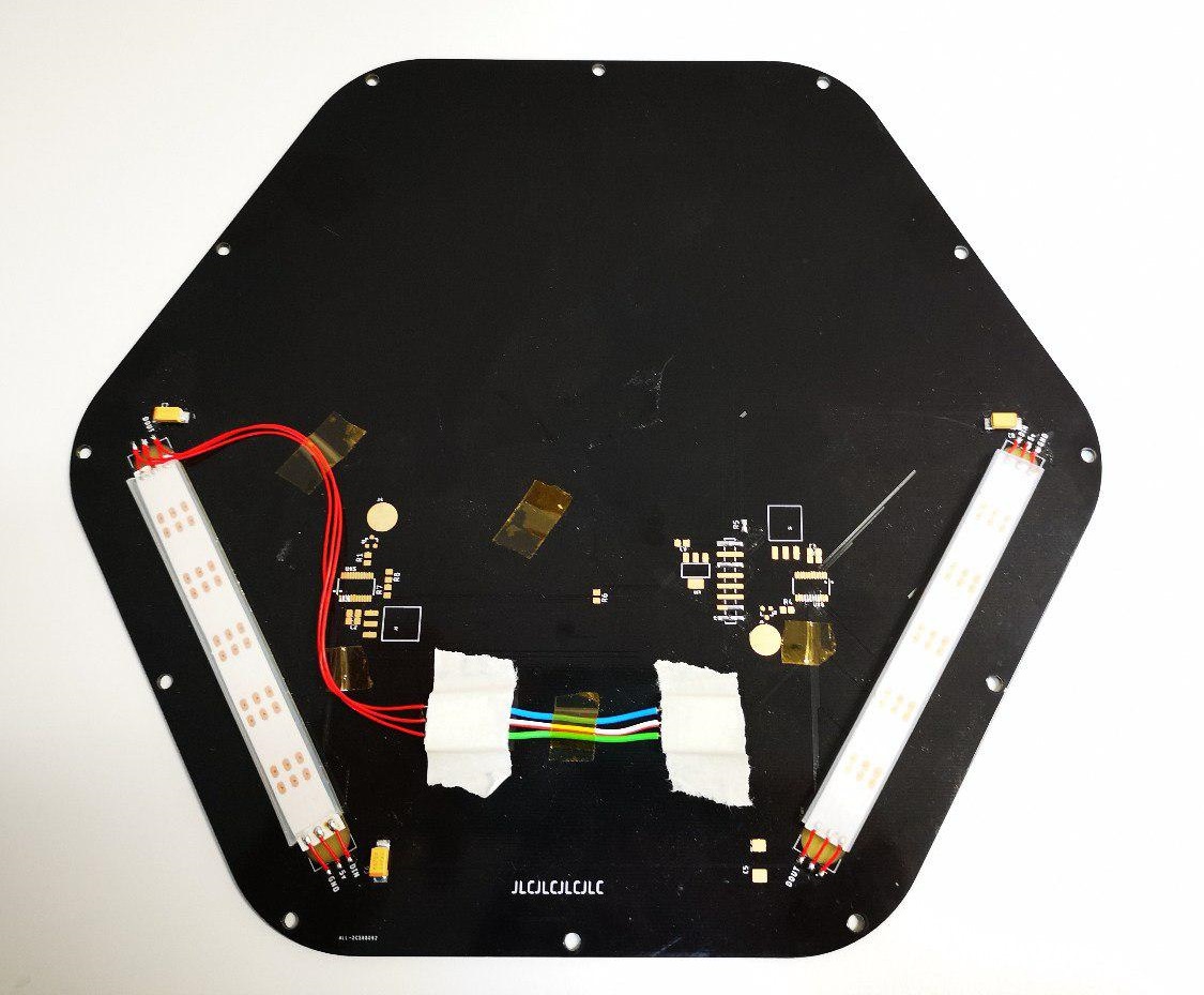
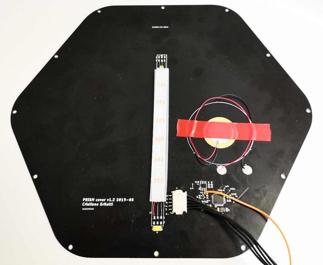
Instead of two separate LED strips and two additional LEDs for the buttons, I used a single central strip, hiding the second LED from the bottom to avoid having to solder many separate pieces of strip like in the early prototypes. It's a waste of a LED, but it dramatically improves assembly time and it's well worth the few cents, at least for the first small production batch.
I also added an ATmega328P to control everything: while the initial idea was to have just the LED strip controlled by the main board, this allows for greater flexibility and a nice gateway to start getting confident in reprogramming Prism. Even if you're a newbie and you're scared of playing with dangerous high voltage, you can still easily and safely customize the front panel with the familiar Arduino IDE. And we have a lot of ideas for that! Like making a Supercar themed version with a horizontal LED strip, a Larson scanner and cool black/gold graphics, or a HAL9000 version with a NeoPixel ring and a speaker to creep you out every time you plug your EV :)
But here comes a big fail: the CAP1203 touch IC doesn't work with a wet sensor, and Prism will be installed and operated outside under any weather condition! We're still discussing about the usefulness of that button (Prism is plug and play) anyway.
However this was a blessing in disguise, as being a big feature creep victim gave me the idea of adding a piezo disc to the cover. This way, we can have both a speaker and a knock sensor!
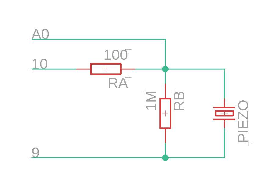
Looking around for inspiration, I only found projects using the piezo as either a sensor or a speaker; I couldn't find any doing both. But that's not hard: I connected the piezo to pins 9 and 10 of the Arduino, with a 100ohm resistor in series to limit driving current and a 1M resistor across it to limit output voltage.
![]() I'm connecting the piezo to two pins to drive it with twice the voltage using the toneAC library. I could barely hear the difference as human ears are logarithmic, but measuring with an app clearly showed double the sound pressure compared with the piezo driven only by a single pin. To sense a knock, we have to pull pin 9 to ground, make pin 10 an input and read the analog value from A0. We just have to wait a few milliseconds for the piezo to settle after playing a note before listening to knocks to avoid a loop.
I'm connecting the piezo to two pins to drive it with twice the voltage using the toneAC library. I could barely hear the difference as human ears are logarithmic, but measuring with an app clearly showed double the sound pressure compared with the piezo driven only by a single pin. To sense a knock, we have to pull pin 9 to ground, make pin 10 an input and read the analog value from A0. We just have to wait a few milliseconds for the piezo to settle after playing a note before listening to knocks to avoid a loop.I was a bit worried about the voltage spikes from the piezo, but the internal ATmega protection diodes seem to be enough to dissipate the tiny currents generated. I was also worried that wall vibrations from nearby passing trucks could generate false knocks, but it turns out that our rubber seals work very well to isolate vibrations too; I added a sensitivity setting to help in noisy environments if needed.
Here's how it works, with some Super Mario nerdiness [source code here]:
And I can also program it to respond to different knock combinations, like this. It shouldn't be hard to write some code to record custom knock sequences!
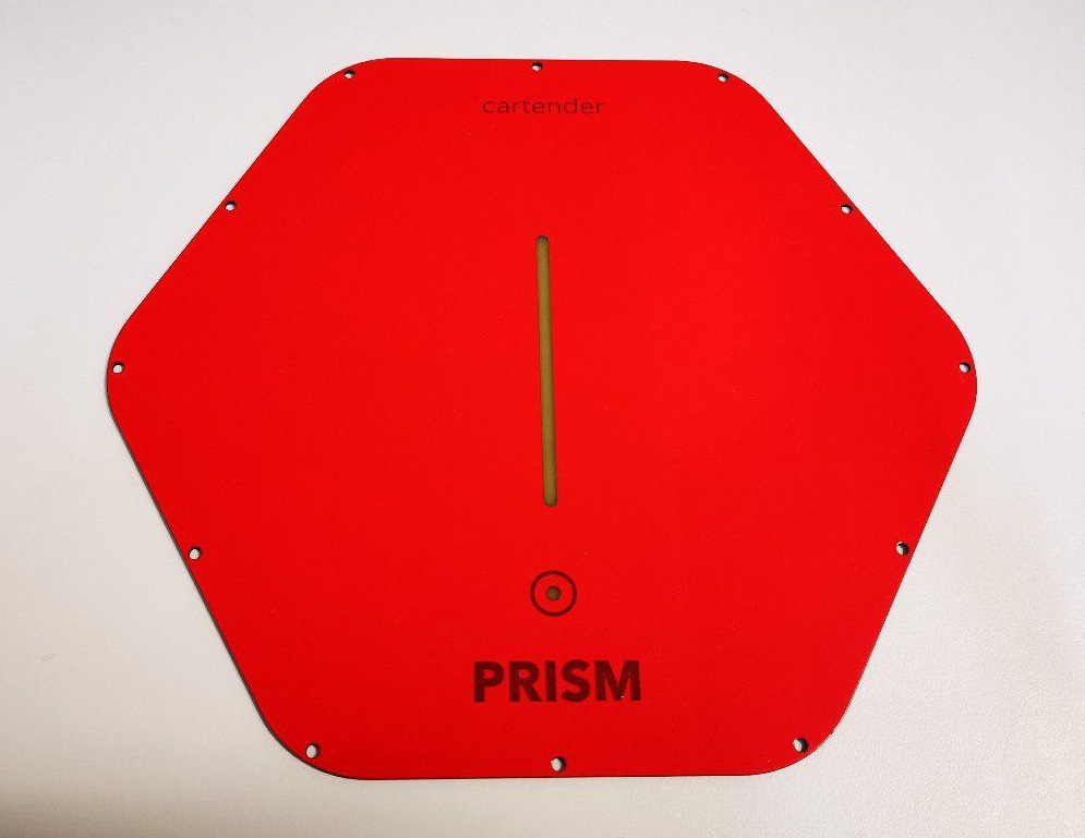
But I also didn't want to give up the touch button yet, so I ditched the fancy ICs and implemented the TouchLib OpAmp circuit with a shielded sensor, that will hopefully work better with water.
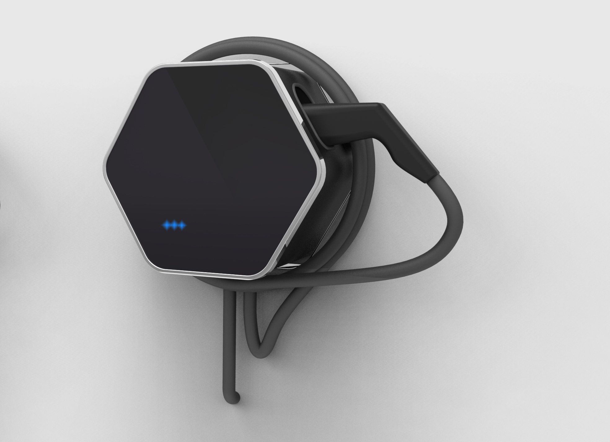
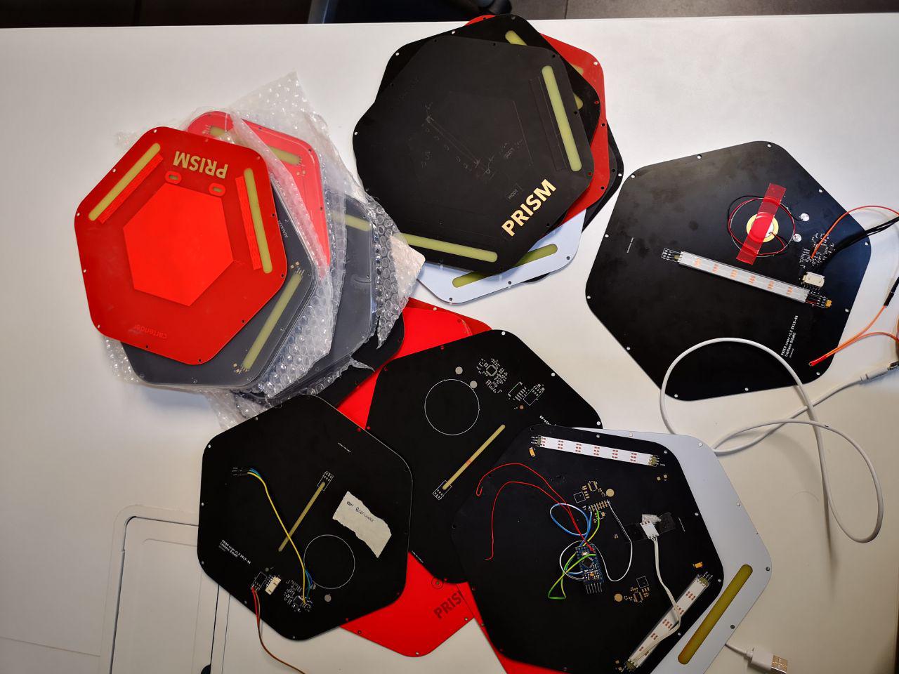
And here it is, the latest version, in all its glory:
![]()
![]()
And it only took a few tries! :P
![]()
Why?
While engineering this cover, I had a big doubt stressing me the whole time. Why does no commercial product have PCBs exposed to the users? Sure, there are a few exceptions, but it's mostly niche stuff. Am I missing something obvious?
There's very few literature online about this, and basically people suggest you contact some external certification laboratory. Which I did, and while they said there shouldn't be any problem, they also said I'd have to bring the product in and pay for testing to get a definitive answer, risking a negative verdict and wasting all the effort made in designing the cover (we're still a team of two working on this, it would kill us). I wanted to be a bit more safe before committing to this, so I contacted the biggest expert on product development I knew: the great Bunnie. Here are the concerns he raised:
In your case, you're just exposing the PCB as a soldermask surface plus copper, with no components, if I'm to understand the videos and photo correctly.
This is /probably/ okay, but here's some of the common reasons why PCBs are never exposed:
1) ESD -- there is a rule for example in the EU, where a product must survive contact with I believe it is an 8kV HBM test zap. "survive contact" is somewhat up to interpretation; for example, if the device reboots, it could be OK, if you put it in the user manual that this is normal operation. But generally, even connector shells are often buried inside of plastic shells because the test gun has a specific shape to it, and by recessing a connector behind 2mm of plastic the gun can't actually contact the metal shell of the connector and thus the circuit escapes exposure to the 8kV HBM test.
In your case, they would try putting the gun right up against your electrodes, and zapping it. Your circuit would need to survive that while powered on and continue to operate "as normal" in order to be importable to the EU.
2) RoHS/Prop 65/child safety. RoHS is relatively easy to pass, but Prop 65 and child safety laws increases the strictness of lead free from 1000ppm to something like 100ppm iirc. It turns out that copper in nature contains over 100ppm lead, so in fact, copper ore found in the ground is a "health hazard" according to the regulation, but never mind. Laws are laws. In the case of a PCB, the soldermask would be considered a "surface coating" (like paint) and if you had to go for child safety protection the testing procedure calls for the tester to take a knife and scrape the surface and test the resulting flecks for lead (the idea being you want to prevent a child from ingesting lead paint flecks). The problem is copper occurs in nature with over 100ppm lead, and so if any copper comes along for the ride with the knife, you fail the
certification. It's too expensive and energy intensive to refine out the natural lead content of copper, so the compromise has generally been not to show copper to users and/or just put a "this product can cause cancer in the state of California" label on the outside.3) Cosmetic finish. Circuit boards aren't normally manufactured for cosmetic finish, so even though a vendor may make a great looking board sample, it's hard to control the color and quality. There are some board vendors that now are specializing in offering pantone color matching of PCBs (King Credie for example can do it, or at least *try* to -- they
aren't as good as a say, a plastic shop, but at least they know what a pantone color is and they try to hit it to within a reasonable degree of accuracy). The silkscreen also tends to have small pinholes in it,
because it's not meant for cosmetic grade finish, just to help assembly workers find where to put components on the board.4) Probably cost and durability. Soldermask isn't an environmentally durable finish, it'll scratch off easily, and as you noted, it may age over time in unexpected ways. I think the first three concerns usually prevent people from even getting to this point.
It's not to say it can't be done! For your application it looks like it could be imminently reasonable. And there are hacks to get around the regulations and laws. Just -- most people find it easier just to throw
it all inside a plastic case and not have to deal with any of this.His answer was definitely encouraging, except for the ESD issue. After a lot of testing I was pretty confident that the PCB alone would have worked, but I'm a coward (and I invested too much on this) so I chickened out and designed an adhesive plastic sheet to cover the front of the PCB. Oh, and there's another reason for this choice: it doesn't happen very often, but sometimes the slots in the layers get aligned with visible markings on the bare FR4 board, clearly visible from the back but barely visible from the front. I can probably arrange something with the manufacturer if I have to order huge quantities, but for now I don't want to risk scrapping a lot of boards so the front adhesive is still the best option, despite costing like the PCB, doubling the cost of this part.
![]()
I have two options here, a great-looking 0.5mm thick sheet that would force me to reduce the PCB thickness to 1.2mm to still fit in under the frame, or a 0.2mm thick one that would barely fit. I should get some samples soon, we will see what looks best!
In the meantime, get the sources and everything you need to design your own custom front panel here! In the repo you can find a version with copy-pasted parts from the Adafruit NFC reader to play around with the idea of embedding a card reader on the cover, but I haven't completed that design yet. You can also play around with the firmware here (hey! help us implement custom knock sequences! :) )
-
Enclosure hell
08/18/2019 at 16:12 • 5 comments![]()
Before going on with the electronics, I'd like to write a bit about the most painful and stressful part of building a product: the enclosure.
---------- more ----------It all started when we pitched the idea to a friend who's a product designer and asked her to come up with some designs. She prepared a few renders, and we ended up going for a nice hexagon-shaped design:
![]()
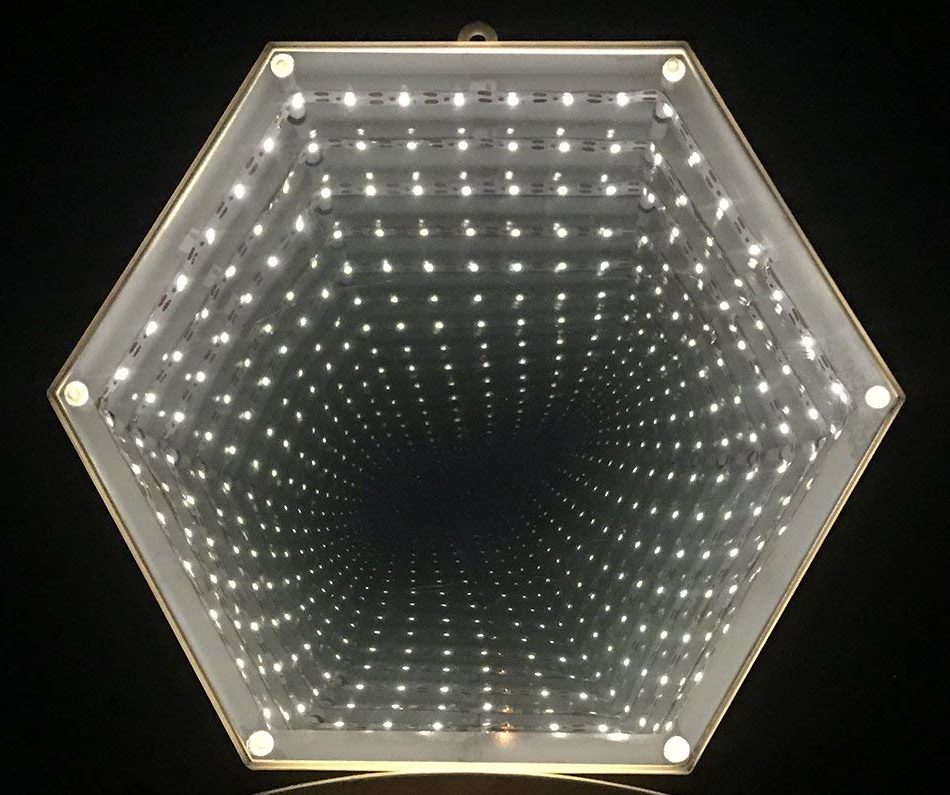
And on top of that, I wanted to add an infinite mirror effect to the cover, with WS2812 RGB LEDs to give users feedback about the status of the charge, like this:
![]()
Other than a great looking, we wanted our enclosure to be water resistant and very strong to resist outdoor weather conditions. Charging stations are typically abused, so we need to make sure our product is rock solid to stand the test of the time.
Great, we have a design idea! Now we just have to build it, starting from simple prototypes to check sizes and proportions. So here starts the journey, with the first fail:
Prototype #1: FDM 3D printed case [fail]
![]()
I don't have a picture of the pieces that I printed, but it turns out it's pretty difficult to print big pieces that fit together perfectly, while pushing the limits of a humble Tevo Tarantula 3D printer. I don't have much experience with Fusion 360, so don't get scared by the ugliness of the design. Long story short, a new solution was needed, so I thought I'd use both laser cutting and 3D printing:
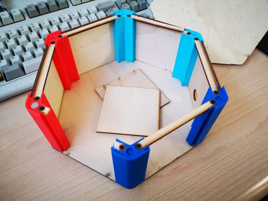
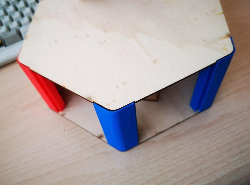
Prototype #2: 3D printed corners and wood [WIN]
![]()
Here I 3D printed only the complex corners; everything else is cut from 2mm plywood. Mixing these rapid prototyping technology makes a lot of sense, as we could better work around the limits of the cheap 3D printer and use the laser cutter to its potential. The bottom is screwed into the pieces, and the sides are slid into the edge slots. On top there's a hole for magnets to hold the cover, and two U-shaped recesses for wood strips to hold everything together. Et voilà, the first prototype was born!
![]()
![]()
We could now hang it to a wall to see if the design makes sense, and test the size of some components. And you can make it too, here's the design!
With everything looking good, we now had to make the next step. But, as any maker with little-to-none experience in industrial manufacturing, we were scared as hell to commit to an extremely expensive plastic injection mold, so we approached Mentec, a company specialized in low-volume enclosures made of machined, folded and glued plastic. Their demo enclosures looked great at the fair where we met them, and I was pretty enthusiast about the potential of this solution. However...
Prototype #3: folded plastic housing [fail]
This seemed like a great idea, as despite the very high price for small quantities, we could use that to bootstrap production and fix bugs and then with the money made with the first sales invest in a proper injection mold. So we sent them our designs and drove to Munich for a meeting to define all the details. We received the first prototypes about a month later, and we were quite disappointed. They didn't look nearly half as good as we imagined, despite the amazing manufacturing quality for an handcrafted product.
![]()
The box is formed by two strips of folded plastic shaped like \_/ and then glued together. Here you can see a detail of that joint, where they milled the strips and then glued them together through the holes inside:
![]()
![]()
In the same way, the perimeter is milled at the right height to fit and glue the bottom sheet. Then a milled hexagon made of a thicker plastic is milled and glued to the upper part of the perimeter, with space for a neoprene gasket and threaded inserts. The front panel is made of a matching hexagon, with a glued transparent window to make the infinite-mirror and slots to fit the other piece of the mirror:
![]()
And finally we have the top bezel, made of a nicer plastic, with slots to mate with the edge underneath, and magnets to keep it attached to the screws:
![]()
The end result is not even that bad, but it's too blocky/squared due to the nature of its construction.
![]()
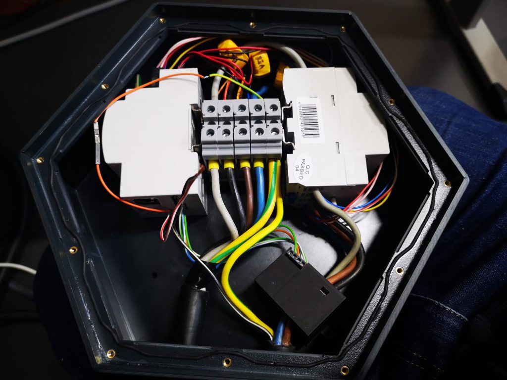
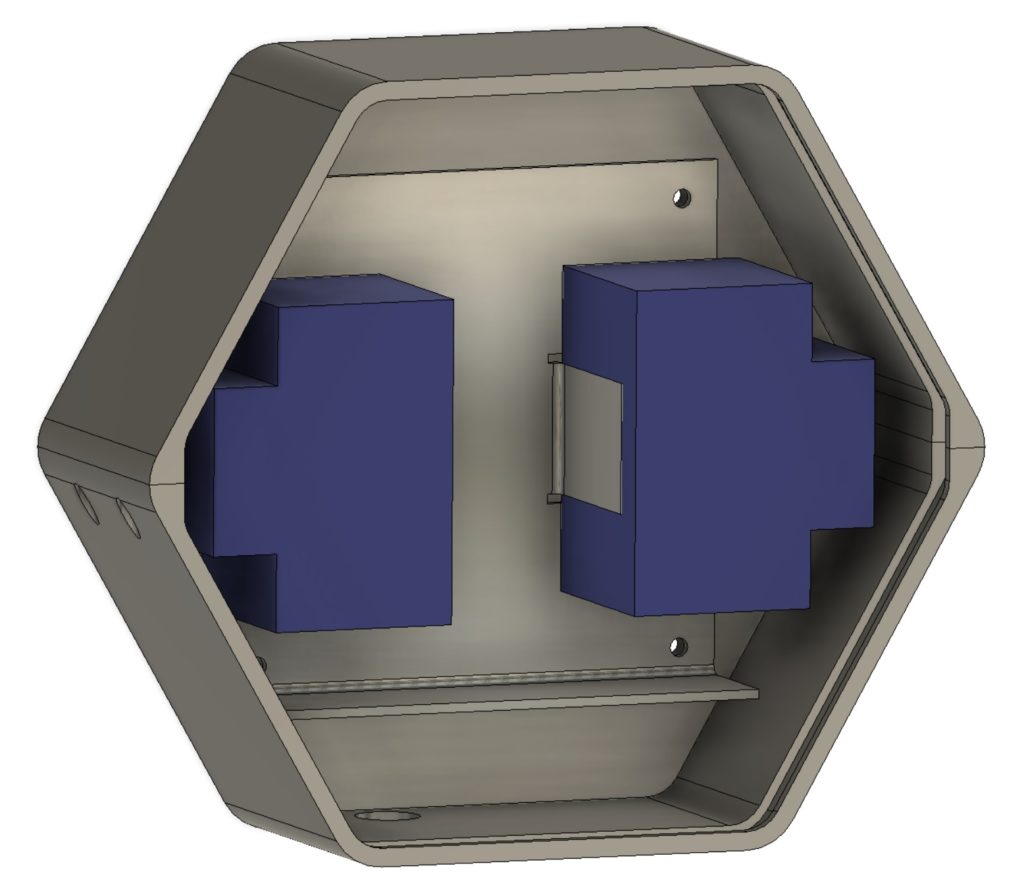
Of course, we knew this solution was a compromise. We started looking at alternatives, but these enclosures at least allowed us to assemble some prototypes to validate the design. Here is a fully assembled prototype, with the electronics fitted inside the DIN box on the left:
![]()
A lot of stuff was still missing, like a way to anchor everything to the base. As you may notice, the placement of the components was a bit unusual too: the idea was to lay the tallest components on their side to save space, especially as the front panel grew quite thick due to the infinite mirror thing. Then we would fold the DIN rail in a U shape and couple it with another rail to hold the screw terminals:
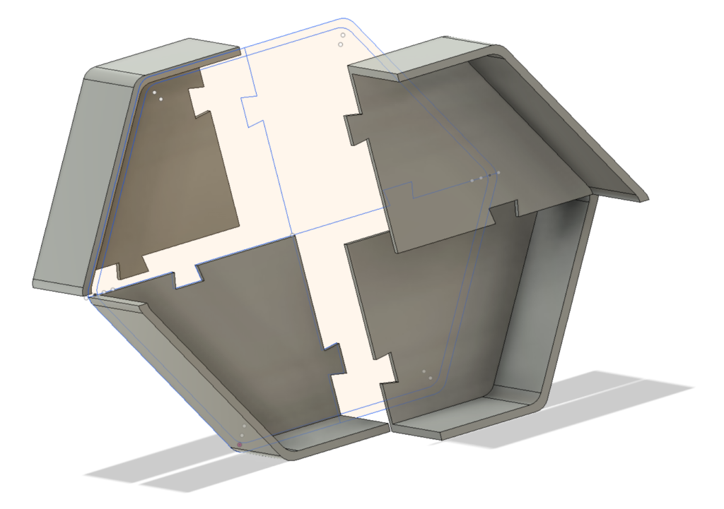
![]() This seemed a great idea at first, but it became soon clear that all of these complications would come back to bite our asses in production. So we made the sensible choice and ditched the infinite mirror idea altogether, simplifying the design by placing all the components upright as they were meant to be. Here I'm testing the new possible layout:
This seemed a great idea at first, but it became soon clear that all of these complications would come back to bite our asses in production. So we made the sensible choice and ditched the infinite mirror idea altogether, simplifying the design by placing all the components upright as they were meant to be. Here I'm testing the new possible layout:![]()
We didn't win this battle, but we definitely learnt a lot. So we went back to the drawing board, and started exploring another crazy idea I had when I was playing with the 3D printer:
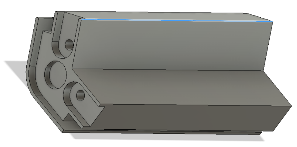
Idea #4: Aluminium extrusion [fail]
If you look back at the 3D printed corners, you can clearly see that they could easily be made by extrusion. I started looking into this really fascinating technology and indeed it turned out to be quite cheap and easy to manufacture. Here's a nice video explaining the process. We had a some options: first was, of course, to make a profile like the one I 3D printed. But then we would have to add metal sheets for all the sides, and machine each piece with holes for the bottom and fittings for the top and bottom covers. A die for this size would cost roughly 3000€, and the minimum quantity is always 1000kg of aluminium at about 3€ per kg.
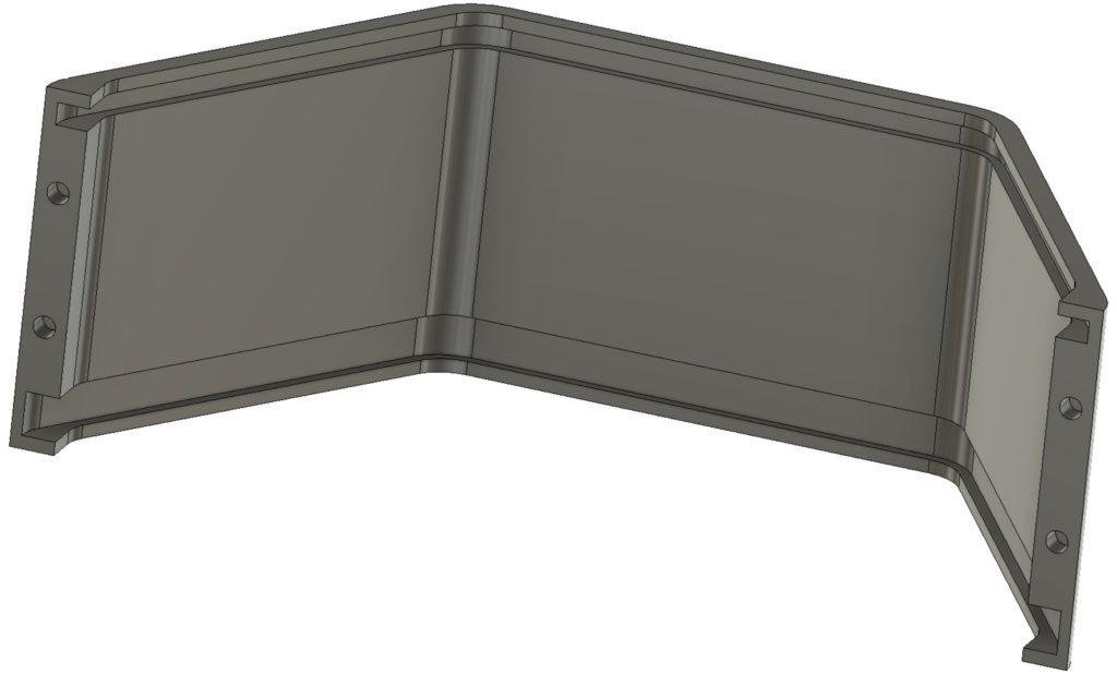
A better option would be to extrude the complete perimeter, but hollow extrusions are super expensive, so the next best thing would be to extrude only half of it and join the two parts with screws; this would ensure robustness and provide an easy way to assemble the final product:
![]()
![]()
![]() Unfortunately there are big drawbacks for this solution too. The back plate would be separated from the wall, but that can easily be solved with a machined (expensive) plate or some pressure-formed dimples if made with sheet steel. We were also worried about bad alignment of the two parts making an ugly visible seam. Despite the cheap extrusion, this method would require a lot of additional parts and machining, increasing the cost too much.
Unfortunately there are big drawbacks for this solution too. The back plate would be separated from the wall, but that can easily be solved with a machined (expensive) plate or some pressure-formed dimples if made with sheet steel. We were also worried about bad alignment of the two parts making an ugly visible seam. Despite the cheap extrusion, this method would require a lot of additional parts and machining, increasing the cost too much.This final experience made it clear that we really needed to go all-in and invest in proper injection molding.
Idea #5: Zama injection [fail]
Looking around and telling our friends about our project, we ended up meeting a company making molds for metal injection, specifically for Zamac alloy. I didn't know much about that, but it turns out it's a great material! It's light, very strong, and more importantly it seems like its molds are cheaper than molds for plastic!
![]() It's impressive the amount of detail you can get with this metal. We worked with the company to get our design made, but after working on the model they couldn't find an easy and cheap way to make the mold without introducing ugly artifacts from the injection points in user-visible areas. It's also not a great idea to build high voltage stuff inside a metal case, despite the good grounding and isolation. But my adventures with Zama are definitely not over, I'll find a way to use this material in a future project!
It's impressive the amount of detail you can get with this metal. We worked with the company to get our design made, but after working on the model they couldn't find an easy and cheap way to make the mold without introducing ugly artifacts from the injection points in user-visible areas. It's also not a great idea to build high voltage stuff inside a metal case, despite the good grounding and isolation. But my adventures with Zama are definitely not over, I'll find a way to use this material in a future project!Final solution: plastic
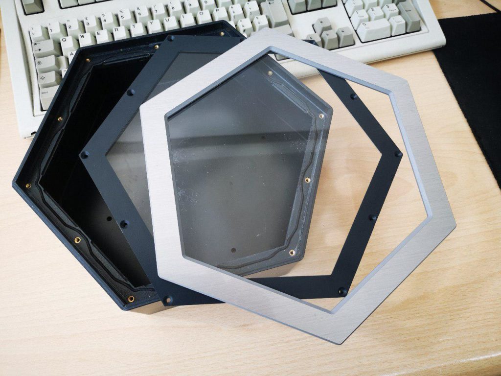
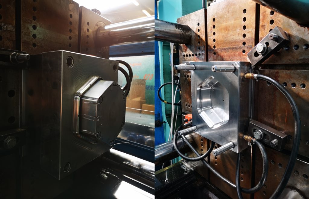
In the end, we had to fight the big monster anyway. But we got very lucky here: a friend pointed to a local company with a lot of experience in this field, Nercos. The very friendly owner spent a lot of time going through every detail and recommended a good consultant that helped us refine the design and prepare it for manufacture. There are some important details that need to be considered, like stress relief points in places where the plastic changes thickness to account for retraction while cooling. There are big constraints too, you have to imagine two separated coupled molds so you can't have undercuts unless you want to pay a lot of money for retractable supports. This is the reason why we didn't build the cable holes into the mold; at least for this first batch, we will drill them with a special fixture that I'm making (more on that when I finish it, it's quite embarrassing at the moment).
After some fiddling we got our first professionally 3D printed prototype:
![]()
![]()
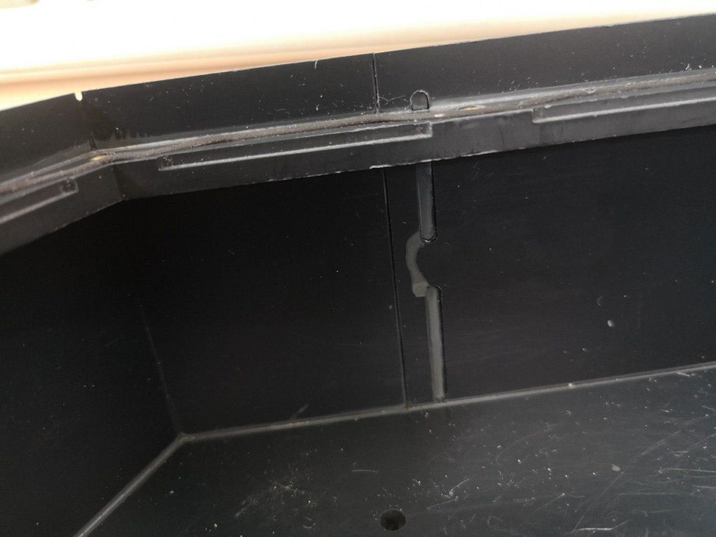
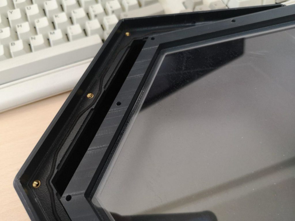
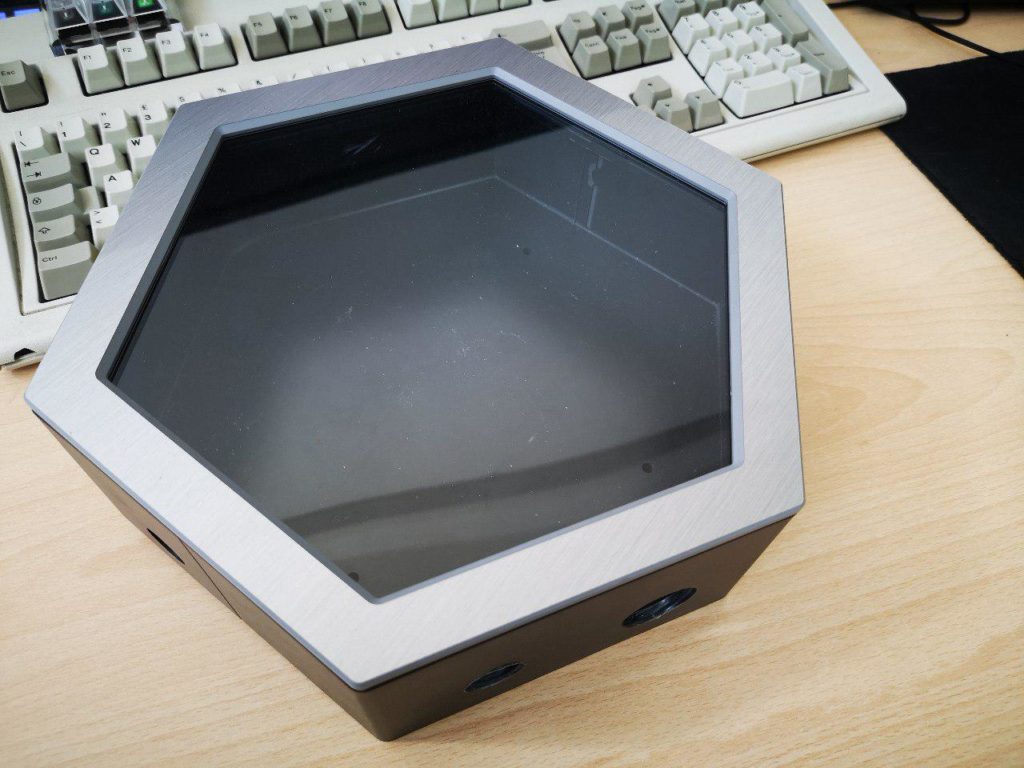
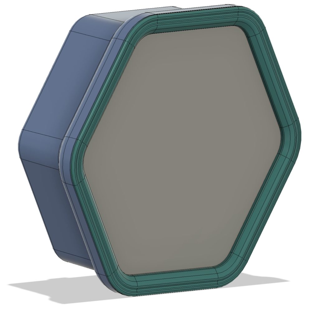
The enclosure will be made of three pieces; the sheet cover will be screwed into the base, with a neoprene ring seal all around, and the screws will be hidden by the top frame that is just snapped in:
![]()
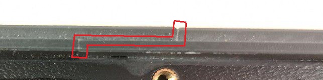
While the neoprene seal guarantees impermeability from the front, to avoid water ingress from the back we created slots on the plastic to snugly fit a rubber grommet compressed with a washer of the same size:
![]()
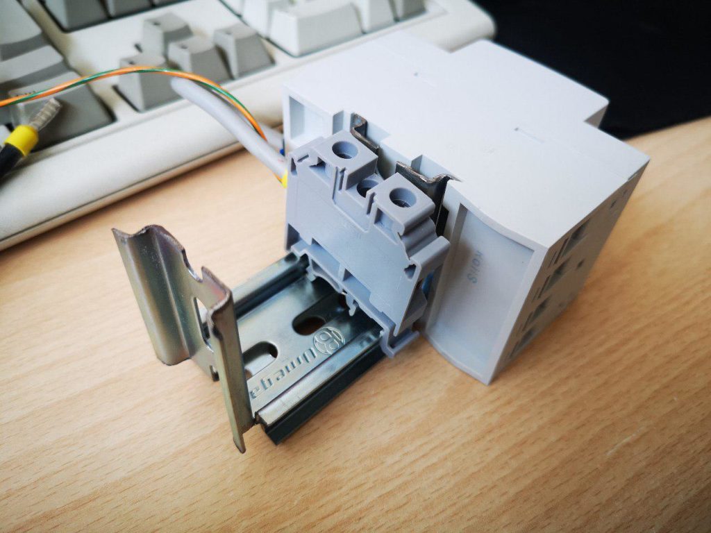
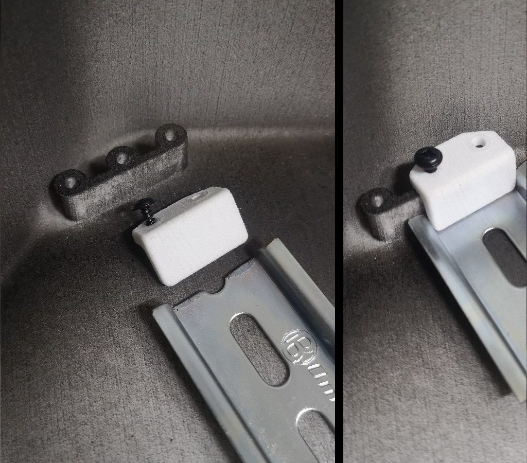
I also found a nice way to attach the DIN rail to the bottom of the box without increasing its thickness and consequently the whole box size, by using L shaped blocks screwed into raised towers to accomodate for the screw length. This way, no space is wasted and everything fits snugly.
![]()
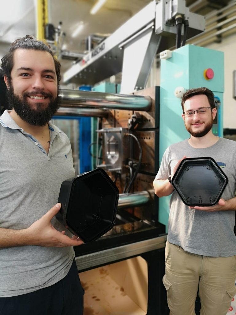
At this point, we got confident enough to jump into the void and get a bank loan to go forward with the mold order. I can't even begin to describe the stress and fear that come from investing way more than you can afford on a single, vital part for your project that can make or break everything. I also have never been in debt in my whole life, so that's another worry I will have to carry for the next few years.
Well, here's the result: my business partner and me holding the first pieces out of the press, tired but happy like giving birth to a baby.
![]()
Isn't it beautiful? And it's all ours!
![]()
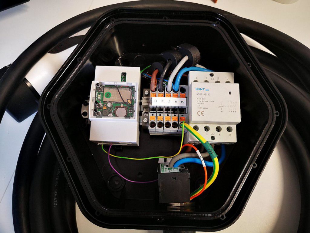
We ran home to test it, and here it is, with all the electronics assembled!
![]()
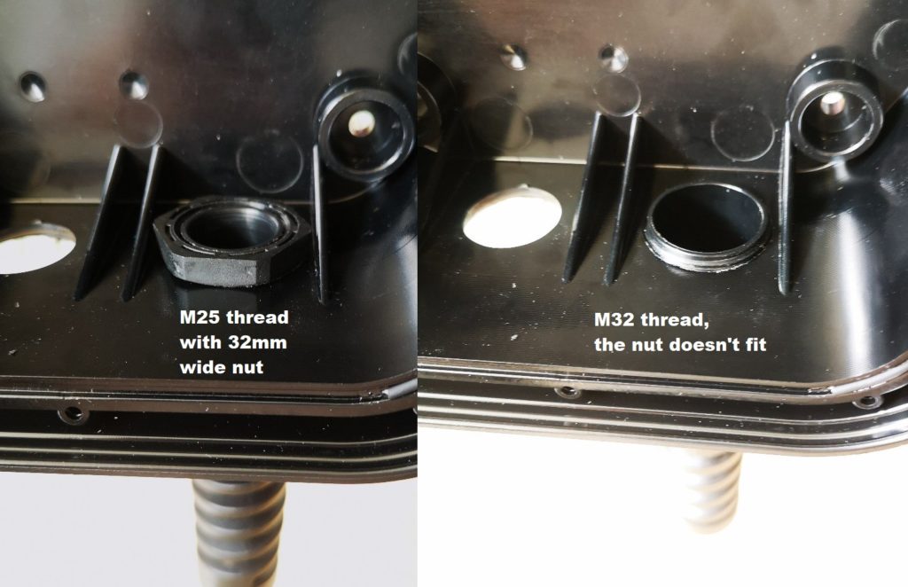
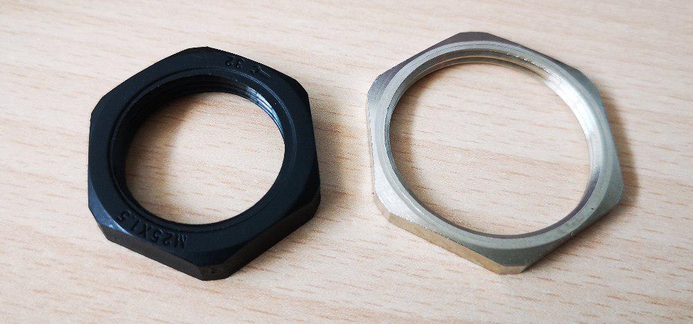
And everything was fine for a while, until we got the latest version of the EV cable samples from the manufacturer. They were 1mm wider than the cables we tested, and didn't fit the spiral cable fittings we used until now! This forced us to look for different holders, but the sizes are standard among manufacturers and most of them stop at 18mm diameter, with M25 threading. The few manufacturers making bigger ones have a M32 threading, that would still barely fit between the plastic reinforcement but only without the plastic nut:
![]()
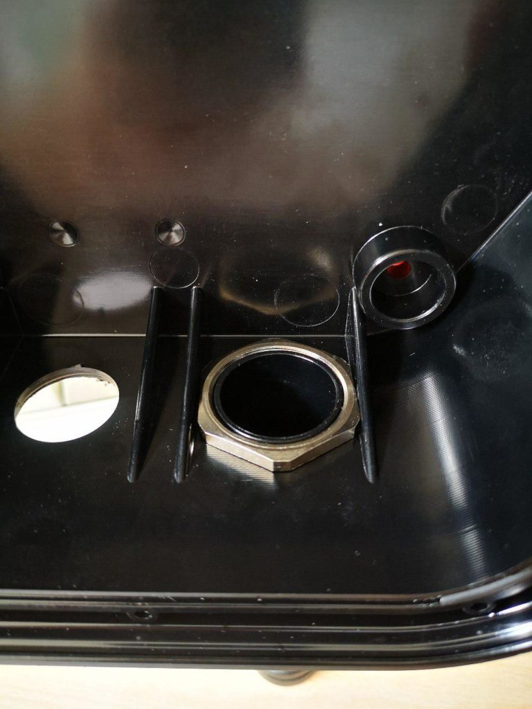
This got me quite worried, as we couldn't modify the molds anymore (well, you can but only by adding plastic, you can't remove existing features). I started thinking about every possible solution, from rotating the box 180° and place the cable on the other side (the plastic reinforcement weren't really needed from our calculations), to milling the existing glands and hope they don't break, to threading the plastic enclosure, maybe increasing its thickness. Then I started reading the fitting manufacturer's manual and found out that they also offer metal nuts, and they have thinner walls than the plastic ones that were delivered with my samples. Measures looked good, so I ordered some, and problem solved!
![]()
It fits!!
![]()
The problem here is that the nut fits too snugly, so I will have to improve my drilling fixture to account for this. We were quite lucky we didn't invest in a special mold with moving parts just to have that hole pre-made, as that problem could have been much bigger.
And here we are, to the present day. You may have noticed I didn't write anything about the cover in this log; that's a surprise that deserves a post of its own.
In the meantime, you can download the CAD files here.
-
POWER!
08/17/2019 at 10:26 • 4 comments![]()
Supplying power to everything is not as easy as it may seem. We need several voltages to power all the components, here’s the budget:
- Isolated from mains, negative connected to mains earth
- ±12V at 14mA per pilot port (0.33W)
- 5V at max. 360mA for the user interface RGB LED strip + up to 40mA per port for contactor relays (0.6W to 2.2W)
- 3.3V at max 14mA for the STM32F103 (0.04W)
- 3.3V at 200mA (with 800mA short peaks) for the Linux module (0.66W – 2.6W peak)
- Referenced to mains neutral
- 3.3V at 23mA for the ATM90E36 (0.07W)
From AC to DC
So we need a total of about 1.8W in normal operation, up to about 5W peak in the worst case. At first I started to look at triple output supplies with ±12V and 5V outputs. Unfortunately, looking around I couldn’t find any triple output module in a reasonable size (and price); it was time for plan B.
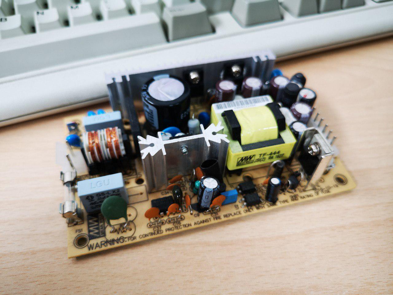
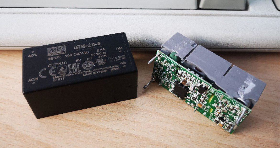
The next best thing would have been to have a single 12V or 5V supply and convert that to all the voltages I needed. Since the biggest load is on the 5V line while the 12V one only requires 14mA, it made more sense to get the 5V output module. Initially the idea was to add way more LEDs, so I started testing with the MeanWell IRM-20-5. This 20W AC supply module outputs 5V at up to 4A.
![]()
±12V Pilot signal supply
Now, how can we generate a ±12V supply from 5V? Looking around for schematics I didn’t find much; most of the circuits are designed for very low current RS232 communication (there are plenty of ICs for that like the venerable MAX232). I could generate +12V with a simple boost converter, and then invert that; however, the only inverter ICs I could find are rated for 5V. The capacitive inverter TC7660S may work, but it’s too close to its absolute maximum rating and its output impedance is way too high.
The TPS65130 is a switching boost converter with an integrated inverter at up to 800mA, but it’s very expensive and requires a lot of (expensive) components to work. The LTC3261 would be perfect if it didn’t cost 6€ a piece (plus the boost converter).
![]()
There’s a nice trick to use a Boost converter to generate both a boosted voltage and its negative; unfortunately switching ICs have a feedback only on the positive line so this wouldn’t work with our unbalanced load. However, since on the Pilot signal the big load is normally only on the positive side, there should be a way to make this work. I have a few ideas that I still haven’t managed to fully explore.
After testing some different solutions, I concluded that the best “compromise” to supply the ±12V rail is to simply drop in a DCDC module like the MeanWell DPU01L-12. They’re cheap, easy to implement and work very well in this application, despite not being regulated.
Isolated 3.3V for the High Voltage measurements
![]()
The holy grail here is the SiLabs Si88341 IC. This device integrates an isolated DC/DC power supply and four channel logic isolation in a very nice package. I don’t know what it is that makes me appreciate this IC so much, but I think it’s truly gorgeous. Unfortunately, it’s not cheap at 5€ in single quantities, plus the transformer, plus the effort to make it work as designed.
![]()
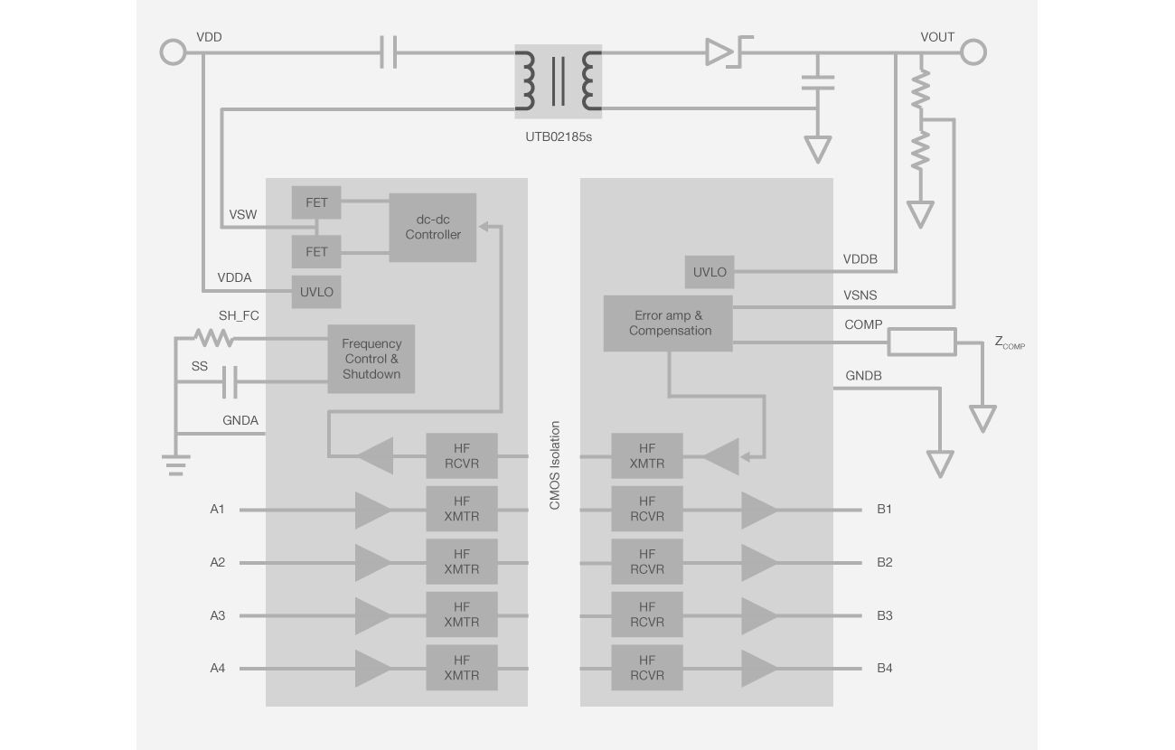
The Isolation Dream Team!
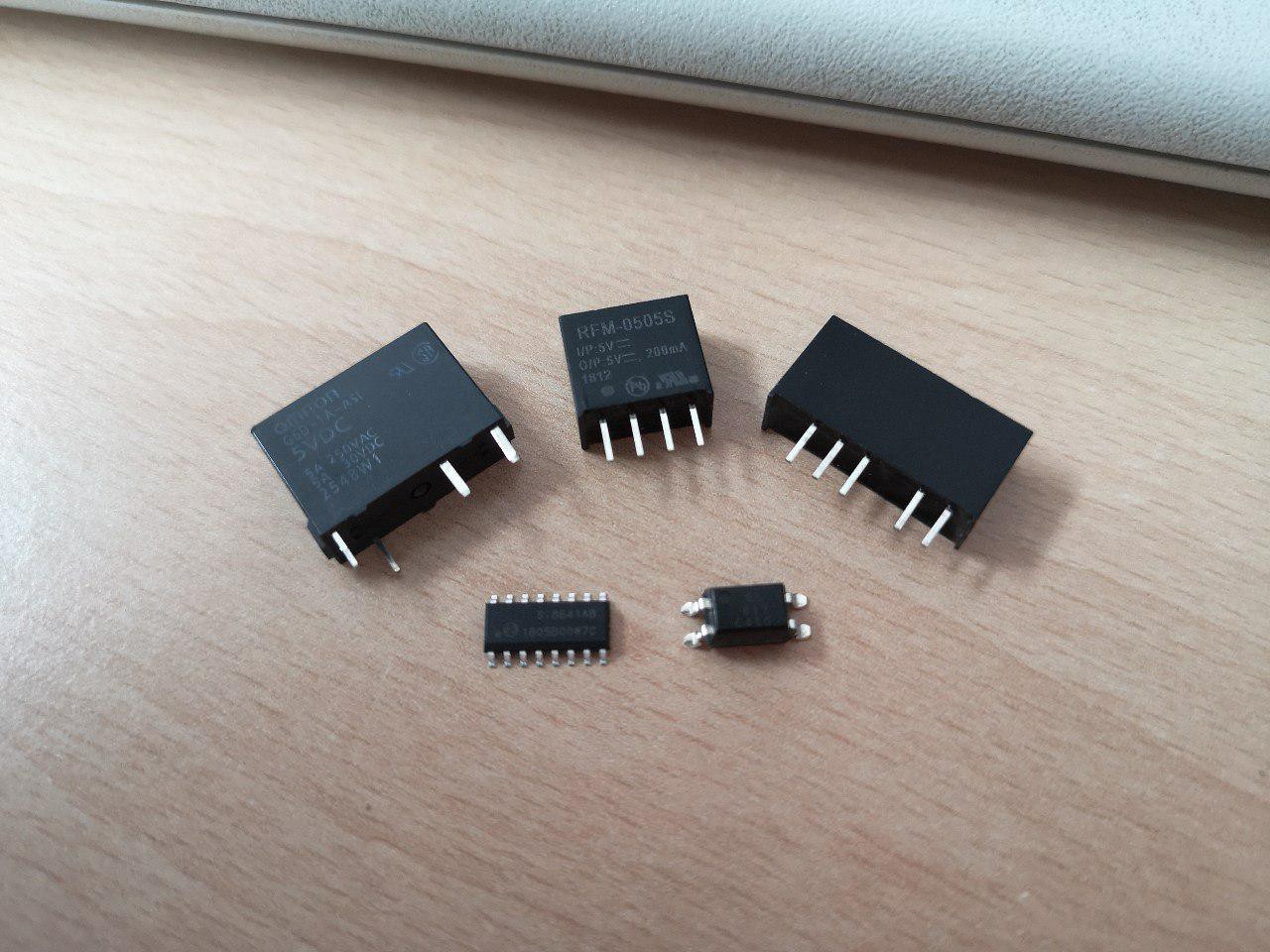
The next best thing is a combination of the Si8641 digital isolator for the signal, and a standard 5V DC/DC isolated module like the RFM-0505S. From there, a simple 3.3V LDO will regulate the supply for the power meter. Easy, lazy, works!
3.3V supply for the Linux module
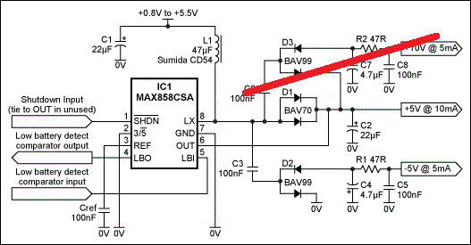
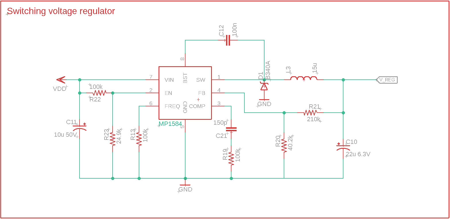
Here the requirements are simple: low ripple, about 200mA continuous with 800mA peaks. Normally I’d just paste here my usual supply block that I used in many other projects, based on the MP1584:
![]()
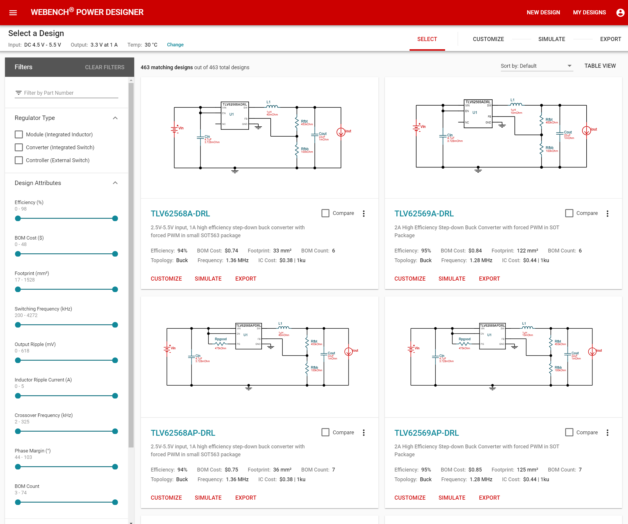
But that design is optimized for a wide input voltage (up to 28V!), while here we have a fixed 5V input and size and efficiency are more important. So I went to one of my favorite online tools, the TI WEBENCH, to find a better part. Here you just have to specify your requirements to get a nice list of options to choose from:
![]()
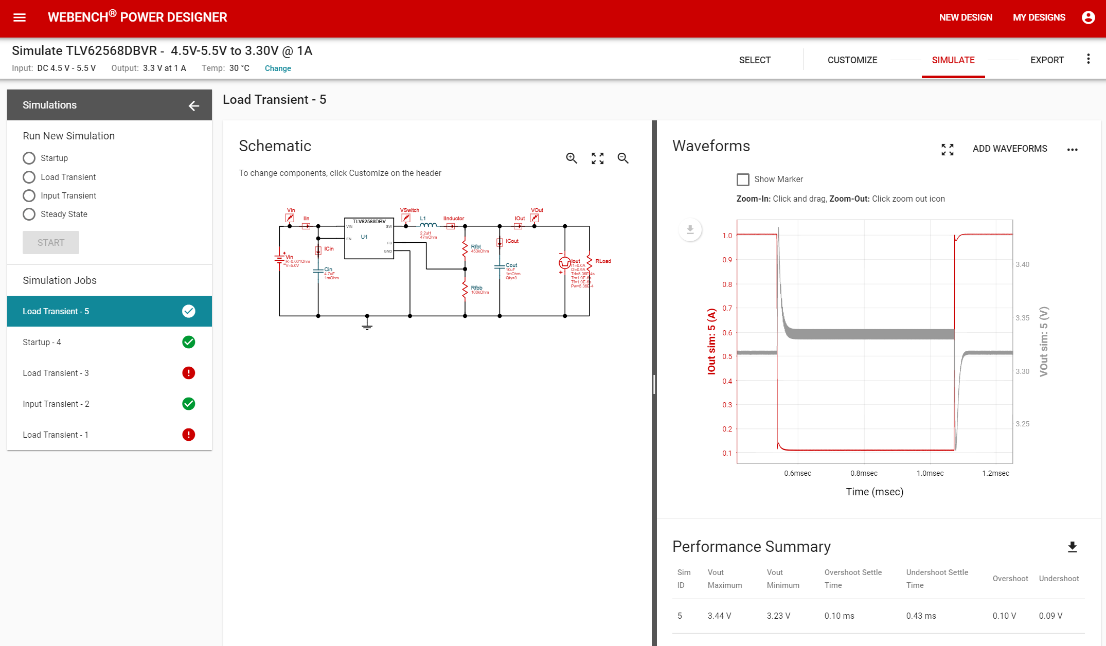
I ended up picking the TLV62568, a nice tiny switching regulator: efficient and cheap. With Webench it’s also very easy to simulate the circuit behavior:
![]()
After testing in real life with various components, I increased the filter caps value and rerouted everything a few times to reduce noise and ripple due to the current spikes from the wifi radio, and managed to get the ripple to a reasonable level.
And that’s it! I’m starting to think that I should have written these posts at the same time as events were unfolding, as reading them again doesn’t make it look like it took much effort to get this project going. Maybe if I wrote them during one of the sleepless nights I had, I would have been able to better show the stress and pain I had to go through!
![]() Enjoy my updated Eagle library with all these components and more!
Enjoy my updated Eagle library with all these components and more! - Isolated from mains, negative connected to mains earth
-
BRAAAINS!
08/12/2019 at 14:18 • 2 comments![]()
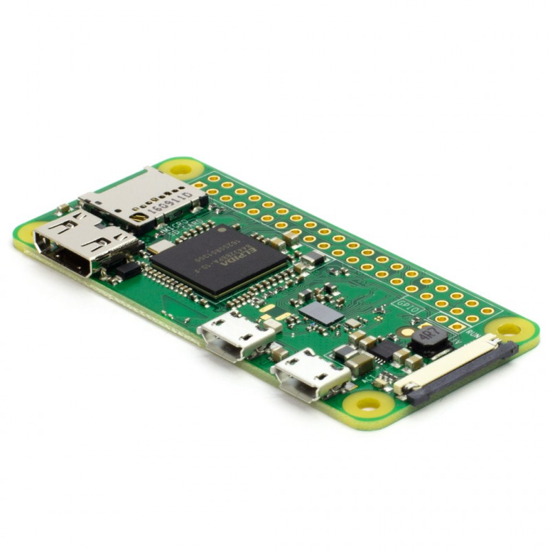
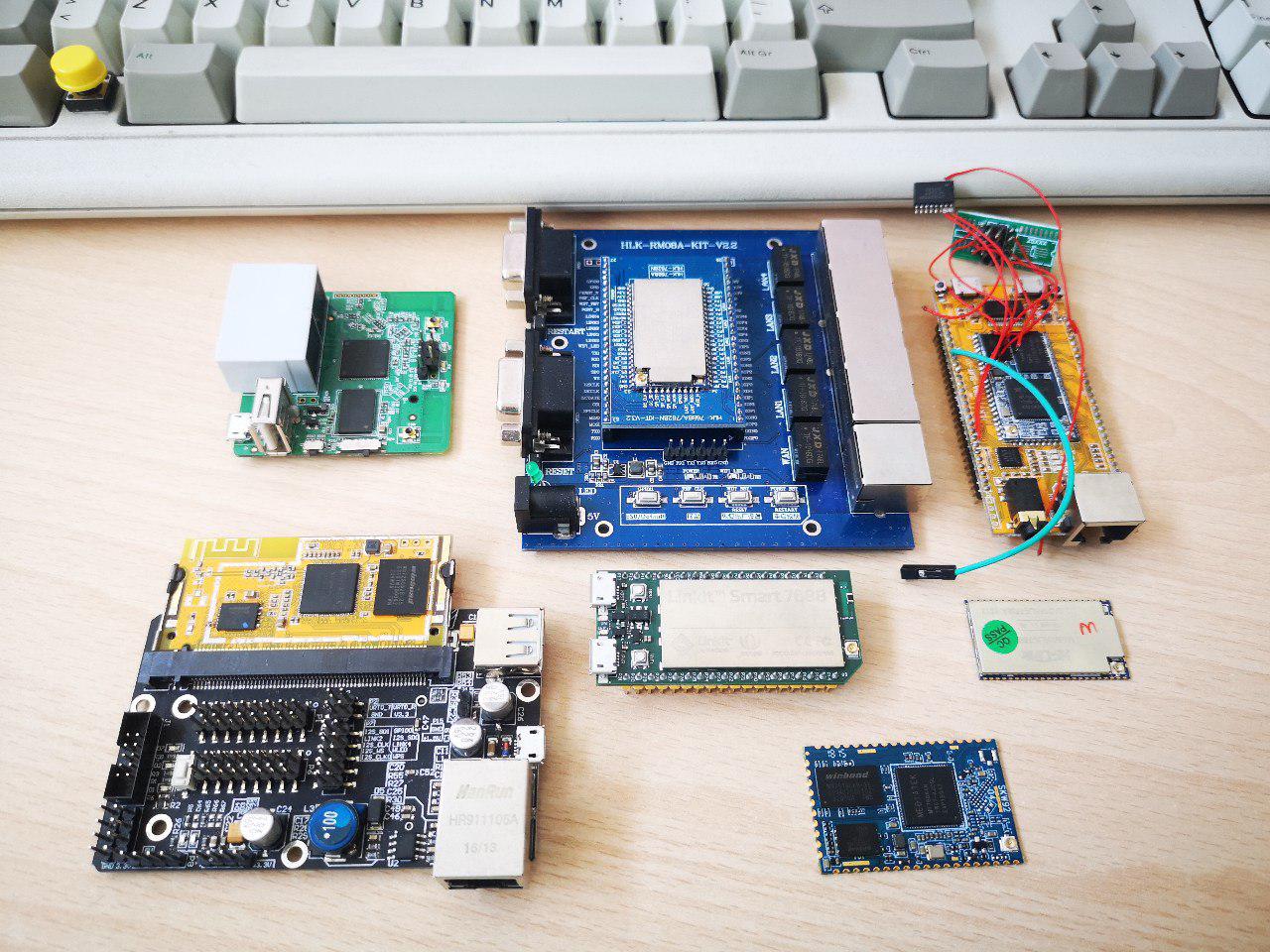
Of course the first thing that comes to the average makers mind when they want to add smart connectivity to something is the venerable Raspberry PI. These boards are great, but almost impossible to find in quantity and definitely impossible to buy at the advertised price if you live outside USA. The only Raspberry I could consider for size and availability is the CM version, but I'd have to add WiFi and Ethernet to the already high price of the board. Finally, they're way overpowered for my purpose. What I'm looking for is the sweet spot between a Raspberry PI and an ESP32 in terms of size, price and features.
So I started looking around for Linux SBCs. There's plenty of choice around, let's look at the best options I tested:
![]()
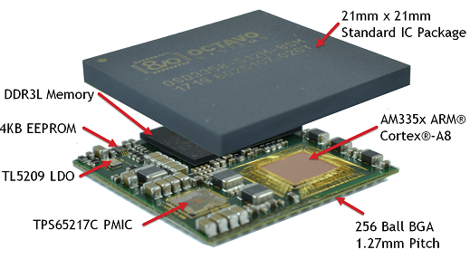
- the Beaglebone is ultra-reliable , and there are awesome SIPs with CPU, RAM and FLASH integrated in a single BGA IC. Octavo Systems really made miracles, but prices are still high and you still have to add WiFi
![]()
- Olimex boards are really nice, but while cheaper they have the same drawbacks of the other SBCs based on TI chips.
![]()
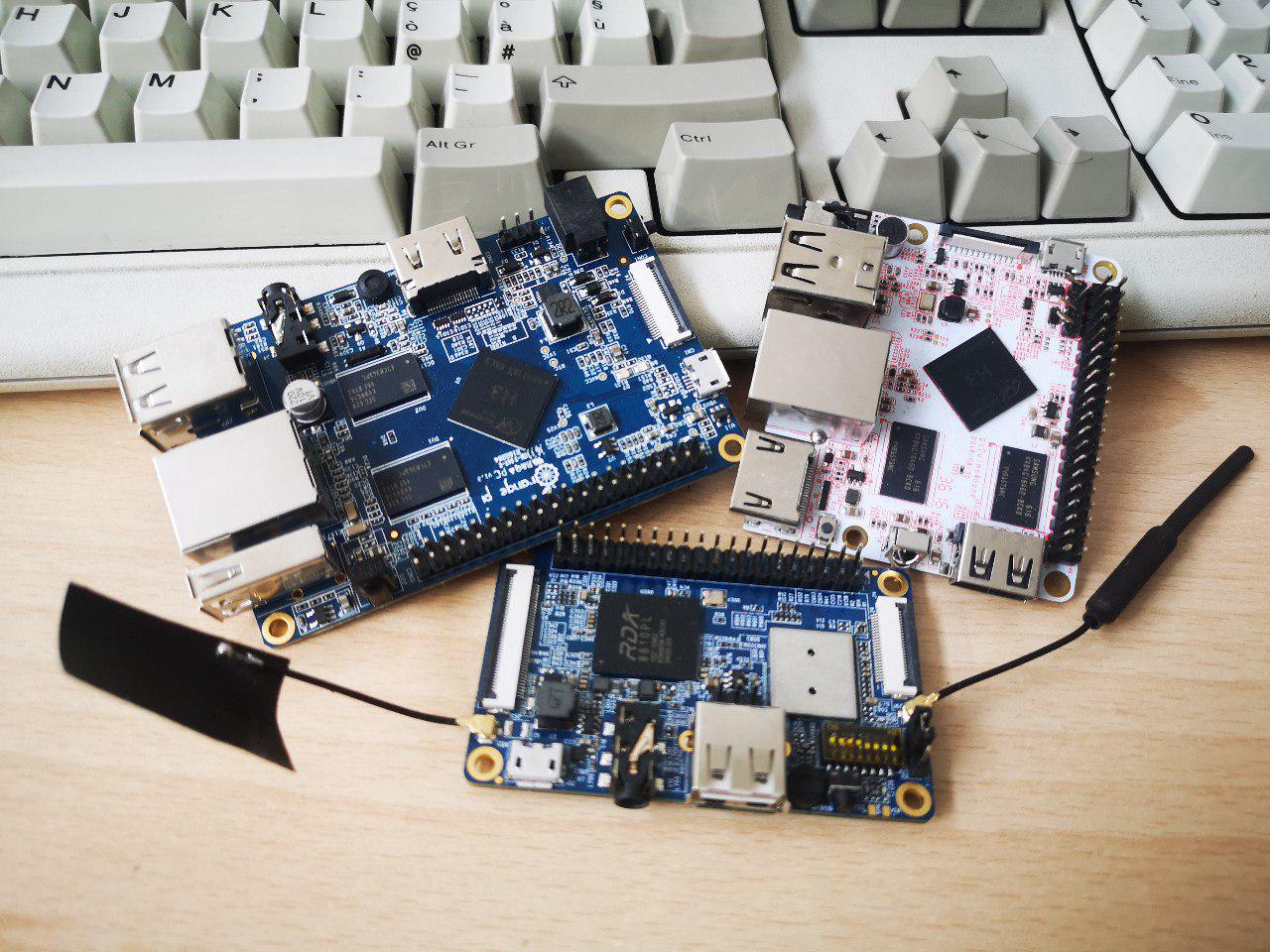
- OrangePI boards are incredibly cheap and have multiple connectivity options! I spent *a lot* of time testing and debugging their Allwinner H3 based boards, and while they work great for your average mediacenter or weekend project, they're definitely not reliable enough for long-term, 24/24 use. Too bad - they had the perfect price point, great features and power, maybe even too much...
![]()
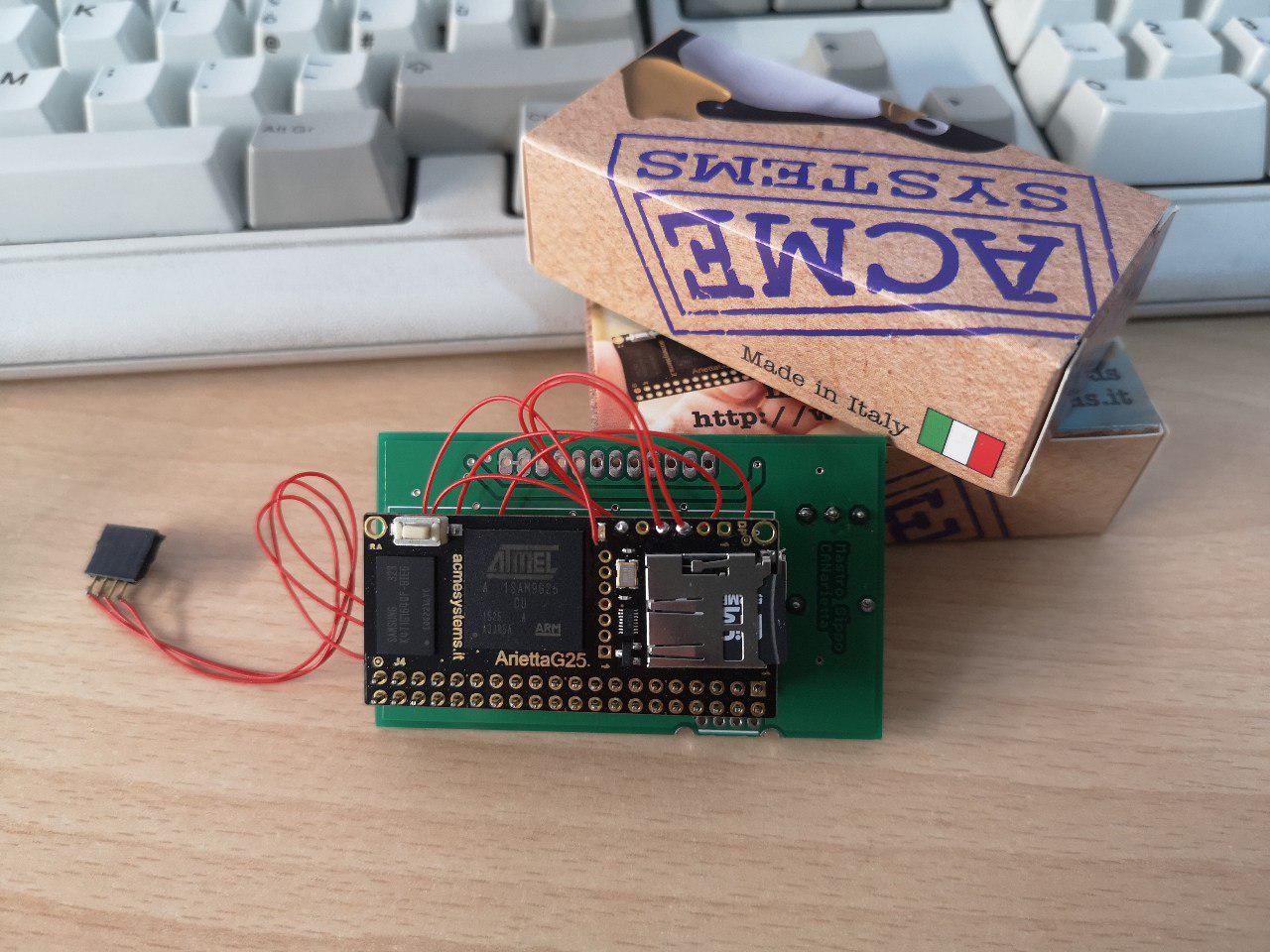
- The gorgeous ARIETTA-G25-V is Made in Italy with high quality and reliable components. I used it for a project in the past, and I really liked it. Unfortunately, its price is still a bit over my budget, especially after adding WiFi and Ethernet.
![]()
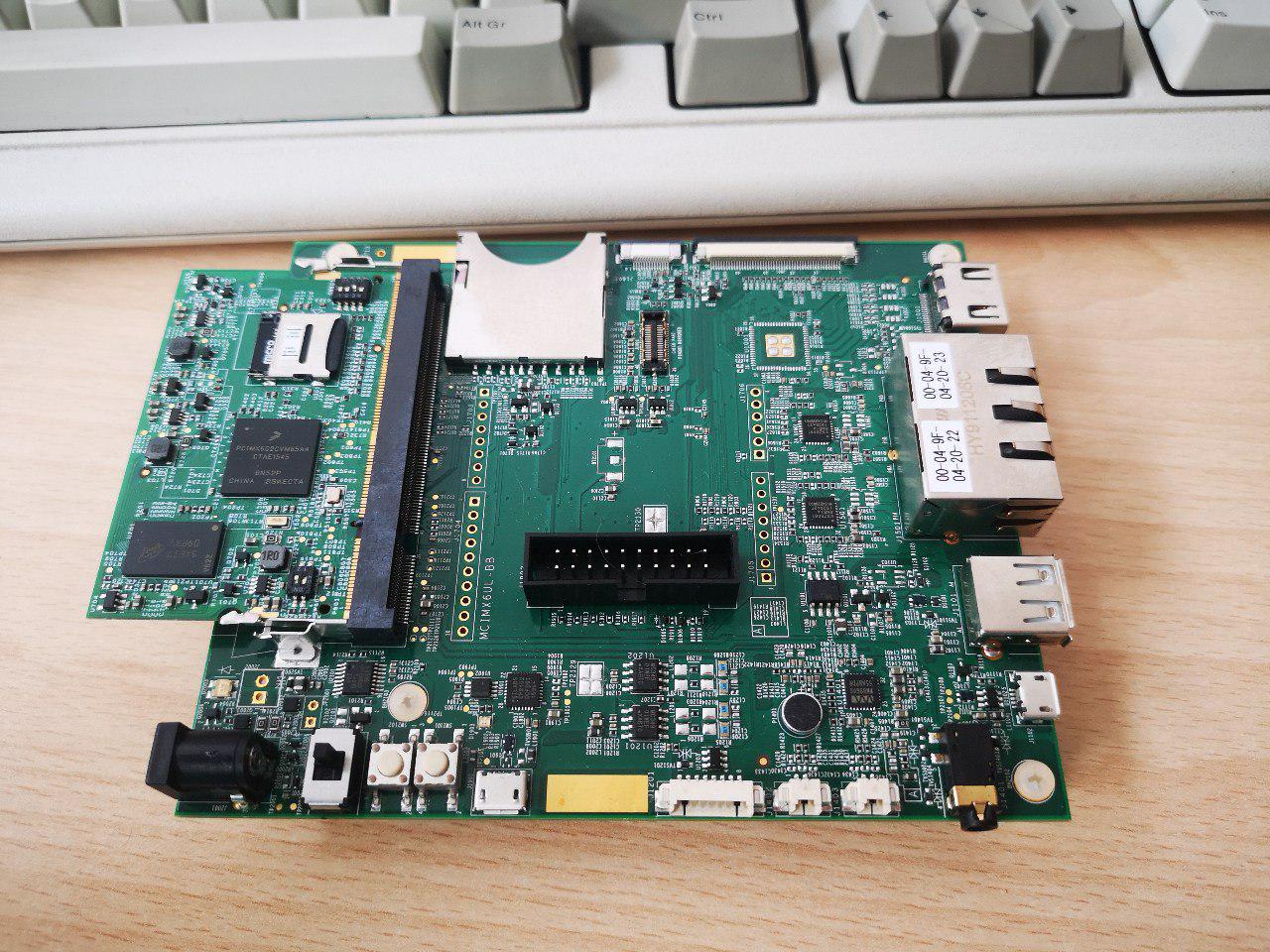
- Freescale/NXP chips are very cool and the choice I'd make if I had more budget or the time to layout an debug complex multi-layer boards. My favorite one for this project was the i.MX6 UL chip: plenty of peripherals, great Yocto support, plenty of third party modules. Unfortunately modules are still quite expensive, but I was really impressed by the power/performance/price/size ratio of the Digi parts:
![]()
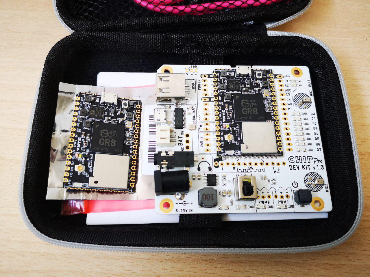
- The GR8 C.H.I.P. was a great choice, but unfortunately the project died. I'll treasure my board as a memento mori.
![]()
What these boards have in common is that they're way overpowered for the task, and priced accordingly. Trying to find a better option, I missed the most obvious one that was hanging under my nose and I was already using daily:
Routers!
I already had a lot of experience with the amazing OpenWRT project. I flashed every single router I've ever owned, built NASes, battery powered drop-boxes to crack WiFi passwords with Reaver, network bridges and more... Routers are great, are very powerful for any application not requiring graphics, are cheap, efficient and very well connected by definition. It's weird I don't see many projects using them around HackADay, kids these days only use those pesky Raspberries... Long gone are the glorious days of the WRT54GL!
![]()
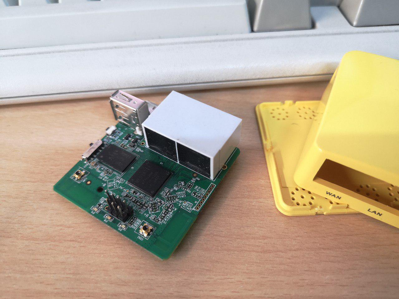
One of the best platform I played with was the GL-MT300N-V2, very reliable and with plenty of CPU power (MIPS24KEc @580MHz), flash (16MB) and RAM (128MB), WiFi, Ethernet, USB host, UARTs, a nice enclosure and certification, for a very low price! It's very well supported by the tiny, rock-solid and security focused OpenWRT Linux distro.
It's based on Mediatek MT7628, a brother of the MT7688AN. You may have never heard of them, but they're the chips powering a lot of maker platforms, sometimes combined with a microcontroller, like the
Arduino Yun, the ingenious WRTnode2R with an STM32F103, the LinkIt Smart7688 with an optional Atmega32u4, the VoCore2, the Onion Omega2, the WiDora Neo and the ReSpeaker. Here's some stuff I tested:![]()
What I love even more of this platform is that after prototyping your design with one of the aforementioned boards, there are many cheap module options that you can easily drop in your design and just work as long as you provide a stable 3.3V supply. At the time, the two best options available were the HLK-7688A and the SKW92B. I tested both, and decided for the HiLink module as it's smaller and shielded. Recently Onion introduced the Omega2S+ in a similar form factor; if it were available at the time, I would probably have chosen this part. I will definitely switch to them after the first batch that already went into production, they're slightly more expensive but it's important to reward who contributes to the community.
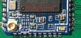
In the meantime, my experience with the HLK-7688A has definitely been positive. Everything worked on first try, except for a big problem: I got the 32MB flash version with a Macronix MX25L25635E that has some issues with 3bytes addressing. Basically, the system sets the flash addressing to 4bytes to use the whole 32MB flash, but the MTK7688 is configured for 3b booting. This is a problem because after a soft reboot the flash would stay in 4b mode and not switch back to 3b, so you have to do a hard reset to reboot correctly. There are a few workarounds for this:
- leave everything at 3b, and only use 16MB of flash. But I paid for 32MB!
- run a script to reset the flash to 3b just before rebooting, but that works only if we do a "controlled" reboot - neither practical nor safe
![]()
- remove the shield and a tiny pull-down resistor inside the module and add an external pull-up to configure the MTK to always use 4b mode. Impractical to do in production at scale.
- add a stronger pull-up resistor at the relevant pin. This kinda worked within a particular range of resistor values, but sometimes it randomly didn't work at all. Too risky for production.
- add an external watchdog that controls the enable pin of the 3.3V regulator, performing a power cycle when necessary
Implementing the last option made a lot of sense for other reasons too, so I went with it. At the same time I tried contacting the manufacturer. I didn't even expect an answer, but incredibly they followed up and quickly fixed their module by replacing the flash with a Winbond part with a different command set that fixed the problem. I ordered a bunch of these news modules to test and they worked! I left the power enable workaround in place anyway, because you never know. Transistors are cheap.
OpenWRT
Using a router firmware has a lot of advantages. First of all, it's extremely compact and efficient: the base system is only 4MB. It's also very well maintained, with constant releases and quick patches for any new vulnerability. After all, you want your router to be as secure as it gets!
And, of course, it's extremely focused on connectivity. This allowed me to easily implement an Access Point mode, that is very useful for EV owners with an underground garage. This way users can monitor the state of charge of their vehicles even if the cars GSM module has no signal.
OpenWRT has a great build system with a lot of very useful packages already ported to the platform. A nice feature is the the stm32flash and avrdude integration to program microcontrollers using the MTK GPIOs. Updates are easily deployed with the internal system; the user is safe from mistakes as the important parts are read-only, and the file system is overlaid to another partition to easily reverse any mistake . I developed scripts to check updates signatures and encrypt communication with the remote server.
We'll talk more about OpenWRT in a dedicated article, where I'll show you how to compile the firmware image, use UBUS for IPC, DTS files and a few tricks I learnt along the way. In the meantime, here's my fork of the distro with the custom files for my module.
-
Measuring power
08/08/2019 at 09:09 • 0 comments![]()
The EVSE decides what's the maximum current a car can draw; this is because only the EVSE knows how it's installed. If it's a portable EVSE, the Pilot signal will limit the charge to the AC plug or cable rating. If it's a wallbox, the installer should have configured it according to the mains wiring specifications. The car should comply with that limit, and the EVSE should disconnect the car if it exceeds it, to prevent fires and avoid tripping the circuit breaker.
Since we already need Current Transformers on each line for this, why stop at measuring current? We can, for example, record power and measure the power factor.
When I started thinking about how to do this, I knew the basics and the theory. Experimenting with the OpenEnergyMonitor and the OpenEVSE, however, showed me that this topic is way more complex than it seems.
Luckily I'm lazy, and as Bill Gates says:
![]()
So instead of using a microcontroller and complex software like everybody does, I looked around and I indeed found a great and easy(er) way to accomplish this task: the marvelous Atmel/Microchip ATM90E36A. This chip is a three-phase energy meter, it also comes as a single-phase version and a cheaper version with less features. It's a full-featured metering IC, measuring all parameters like Vrms, Irms, mean active / reactive / apparent power, frequency, power factor, phase angle, Total Harmonic Distortion (THD) and Discrete Fourier Transform (DFT) for the harmonic component. Everything is exposed via SPI, and there are programmable alarms for voltage sag, phase loss, reverse voltage/current phase sequence, reverse flow and more.
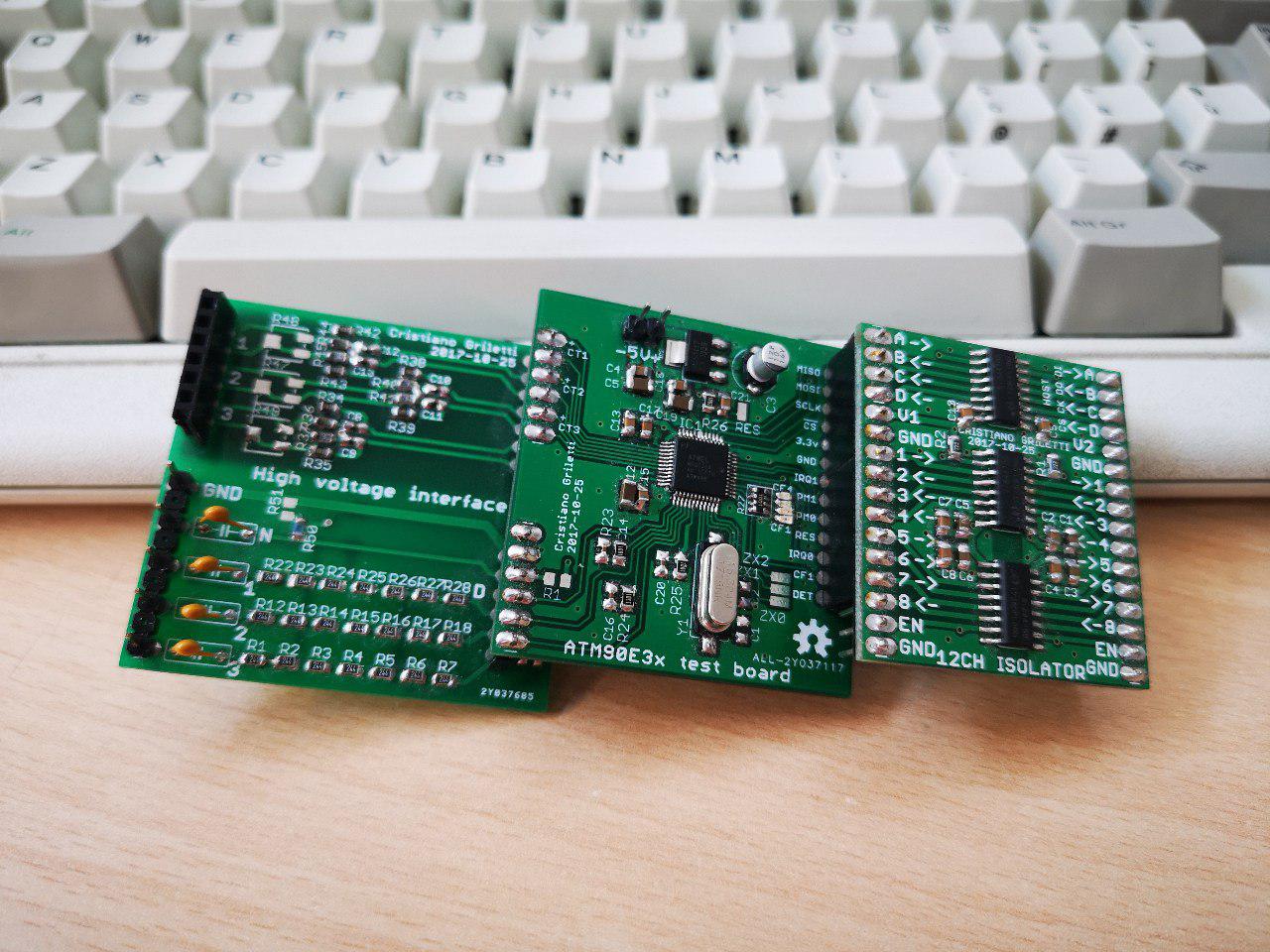
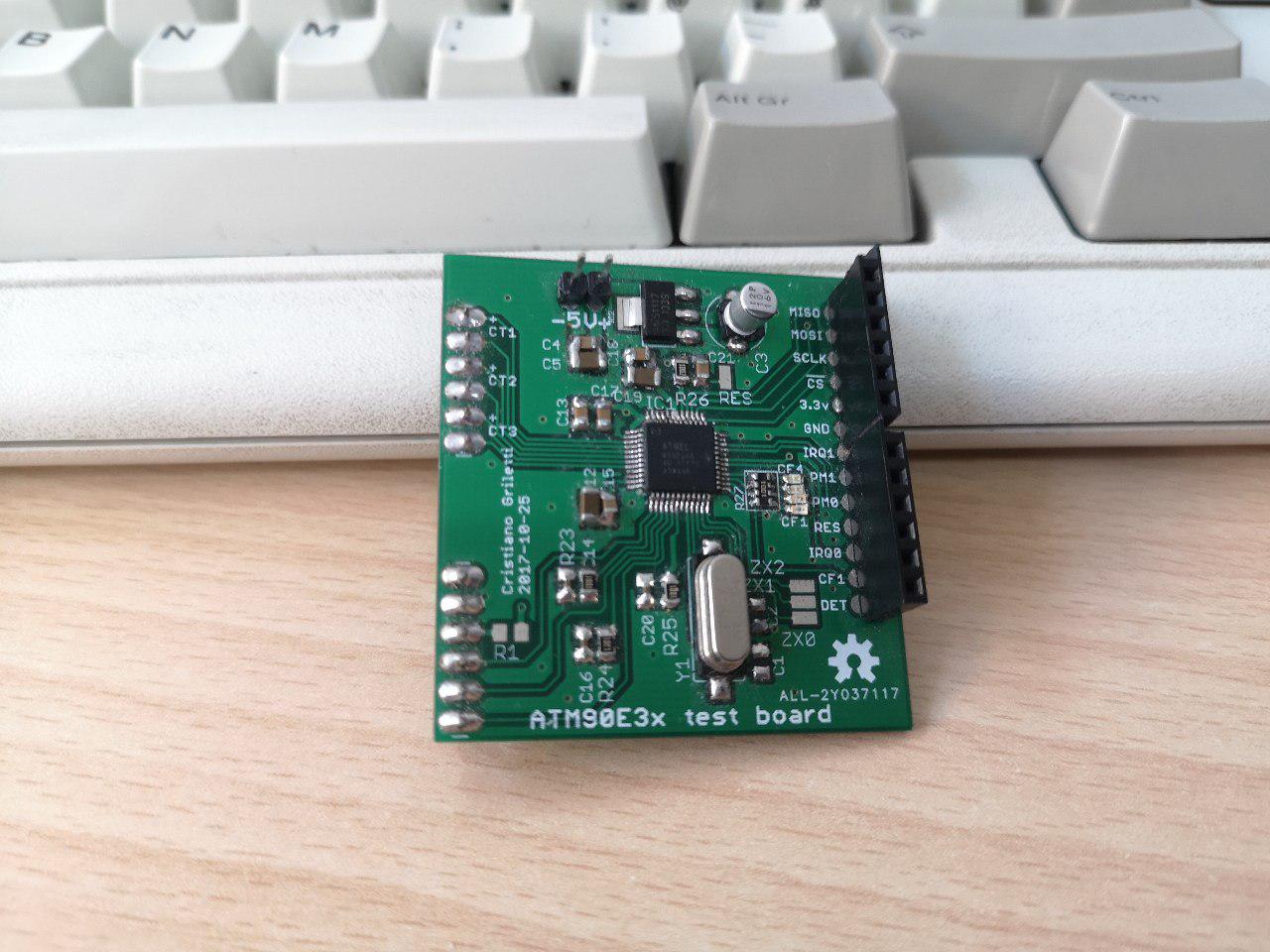
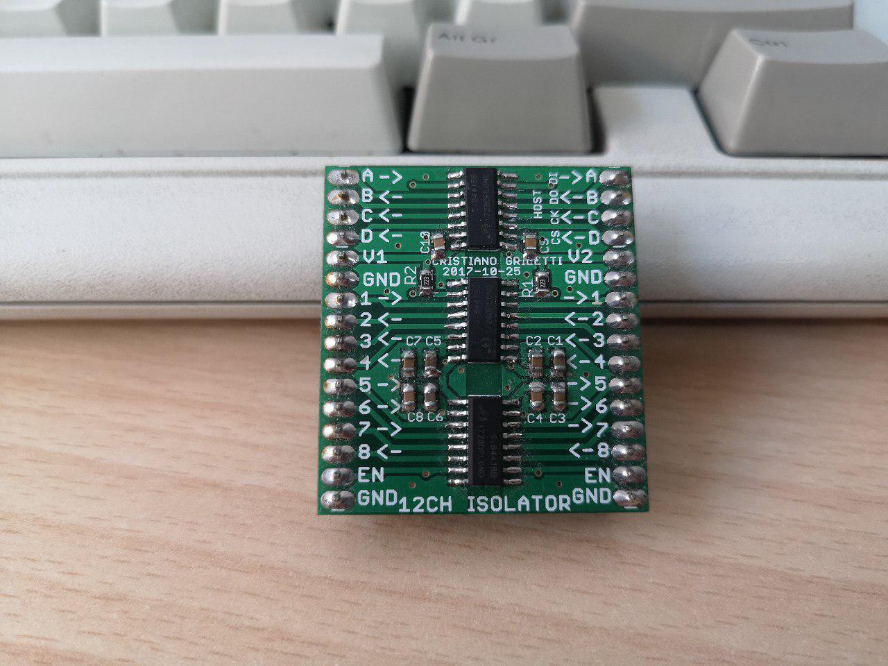
Still following the 5x5cm board module philosophy, I designed three cute boards to experiment with this IC.
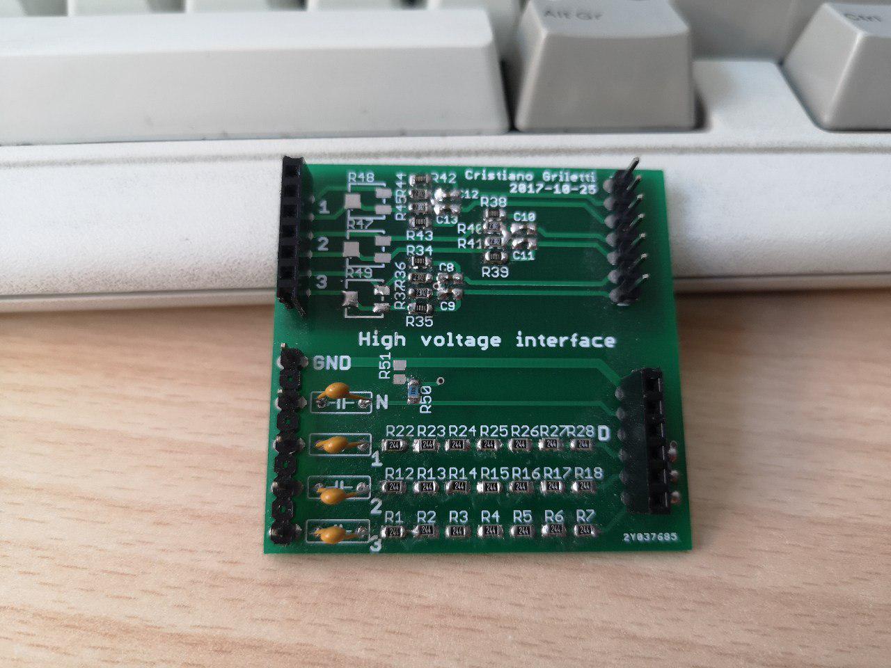
![]() The high voltage input board
The high voltage input boardThis is simply an interface board with proper conditioning for the current transformer and a voltage divider to measure the AC line voltage. Nothing to see here! Sources here.
![]() The ATM90E3x breakout board
The ATM90E3x breakout boardThis board collects all the passives needed to run the ATM90 IC. It has to be powered from an isolated 5V supply from the top pins; I just used a USB phone charger for this. There's space for two capacitors for the crystal; they're not required as the IC has internal caps, but different crystals may require some adjusting. Sources here.
![]() The 12 channel isolator
The 12 channel isolatorLooking for options to avoid bulky optocouplers, I stumbled across the great Si844x. These chips have four capacitive isolated digital I/O each, and are great for our SPI application. Adding two more ICs brings the total I/O count to 12, so I can read the other outputs from the ATM90 and reset it. This board will definitely come in handy for a lot of other projects too! And it's breadboard-friendly! Find sources here.
I'd love to write a long explanation of this three-module circuit, but there's really not much to say: it's the lazy route, we just have some signal conditioning, basic passives and an isolator. The software part is a bit more complex though.
Some software
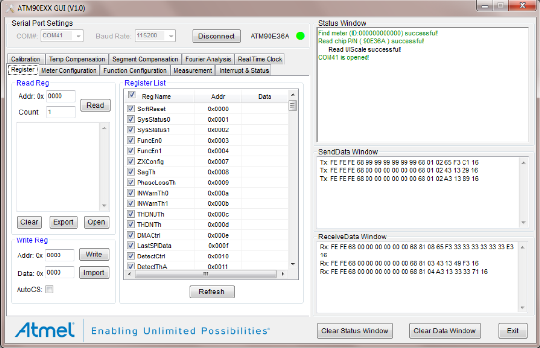
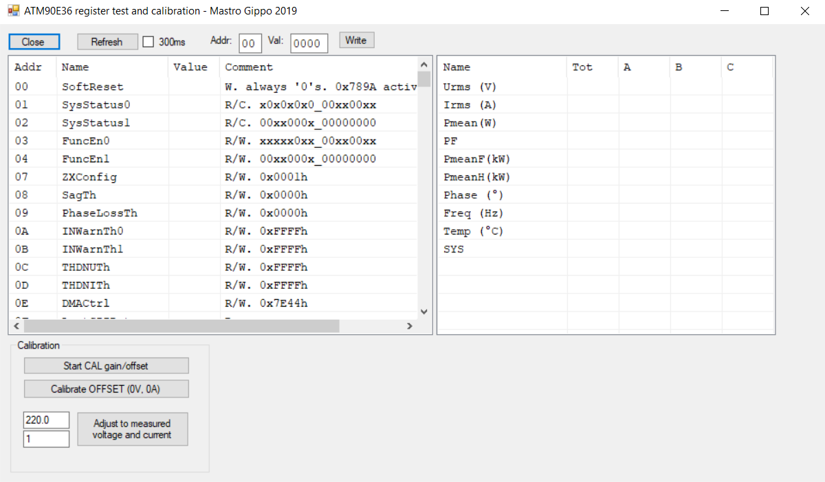
Atmel made a really nice board to test the ATM90E3x chips, the M90E3x-DB. This board is a design reference for a smart meter. I features a microcontroller connected to the ATM90 IC, with some basic software to drive a display and communicate via the serial port. It's super expensive though, so I requested the sources to Microchip and they kindly provided a copy of all the documentation. That includes a very nice software, ATM90ExxGUI.exe, that helps reading and interpreting all registers, and testing and calibrating the IC:
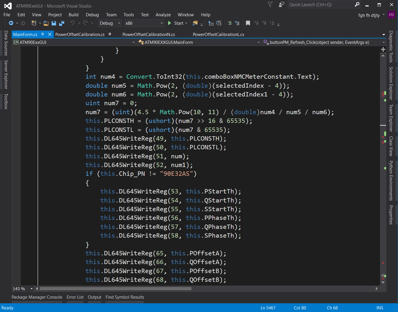
![]() But wait... What's that protocol?? I spent a lot of time analyzing it; luckily there were a lot of screenshots like this one in the documentation so I could at least start to copy requests and answers to emulate parts of the conversation. Reading further in the documentation, I found out that "The GUI adopts user-defined DL/T645-1997 communication protocol." This is an ancient protocol especially designed for communication with energy meters. The only useful documentation I could find is this, and it only describes a lower layer so it doesn't help much with the custom commands for this board. There are sources for the firmware of the demo boards microcontroller, but they're very messy and badly documented. Luckily the GUI program is written in .NET, so a simple decompiler can convert it back to its source, ready to be debugged, modified and recompiled.
But wait... What's that protocol?? I spent a lot of time analyzing it; luckily there were a lot of screenshots like this one in the documentation so I could at least start to copy requests and answers to emulate parts of the conversation. Reading further in the documentation, I found out that "The GUI adopts user-defined DL/T645-1997 communication protocol." This is an ancient protocol especially designed for communication with energy meters. The only useful documentation I could find is this, and it only describes a lower layer so it doesn't help much with the custom commands for this board. There are sources for the firmware of the demo boards microcontroller, but they're very messy and badly documented. Luckily the GUI program is written in .NET, so a simple decompiler can convert it back to its source, ready to be debugged, modified and recompiled. ![]()
Thank you Atmel for not stripping function names! :) At this point I pretty much figured out the protocol, so I programmed an STM32F103 to understand it and send the relevant commands to the ATM90 SPI.
You can find the PlatformIO mbed sources for the STM32 here, but Atmel programs are copyrighted so you'll have to find them yourself.
Calibration
The Atmel software is really nice, but there are a few bugs that make it harder to work with. It's also closed source; I reversed it and could work on improving it, but then I wouldn't be able to share it, so I wrote my own version with
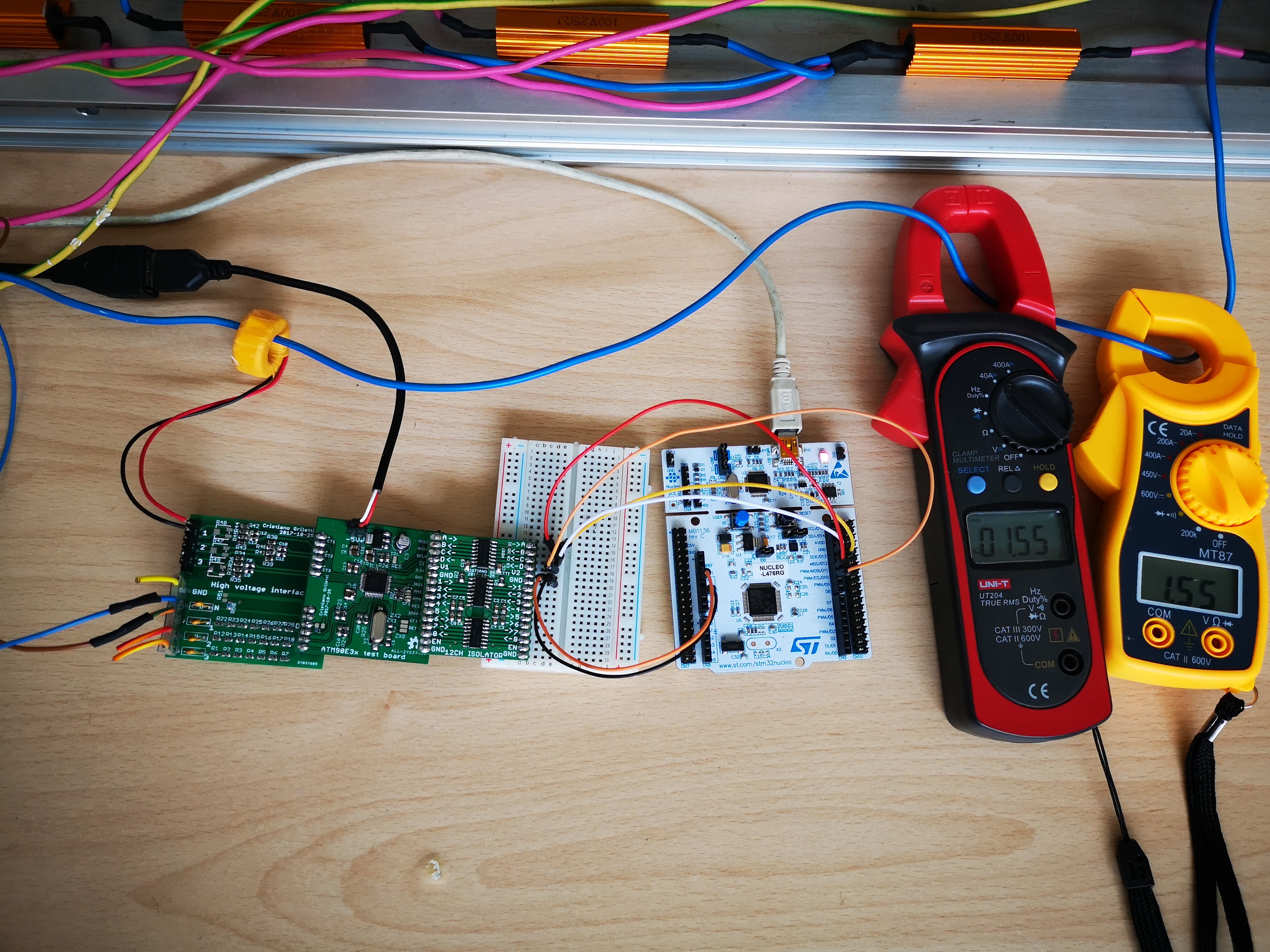
blackjack anda better serial protocol.![]() Now I can get live data from the meter IC and start working on the complex calibration process. At first I started testing with a space heater, then I got serious and built a dummy load with a bunch of 100W resistors screwed on an aluminium profile. With a fixed 150ohm resistance and a perfect power factor, I wrote some code to calculate offset and multipliers and automate calibration. I did these tests a long time ago and I took no pictures, but here's what it looked like:
Now I can get live data from the meter IC and start working on the complex calibration process. At first I started testing with a space heater, then I got serious and built a dummy load with a bunch of 100W resistors screwed on an aluminium profile. With a fixed 150ohm resistance and a perfect power factor, I wrote some code to calculate offset and multipliers and automate calibration. I did these tests a long time ago and I took no pictures, but here's what it looked like:![]()
You can download the C# sources here and the STM32 firmware here! Have fun!
-
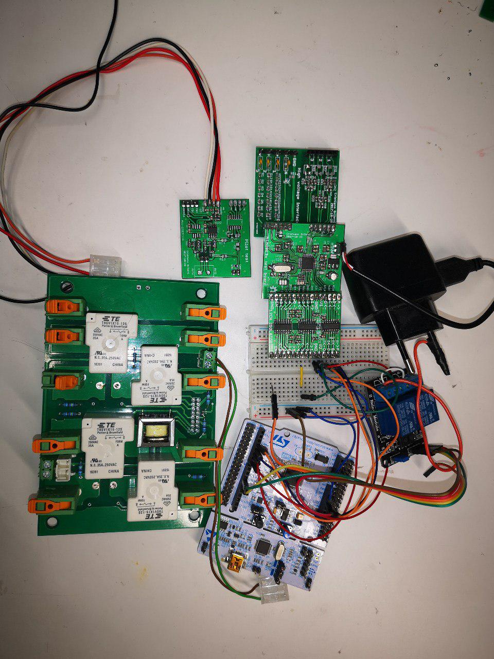
First prototype and test hardware
08/06/2019 at 14:47 • 1 comment![]()
The basic building blocks of an EVSE are pretty standard. We start, of course, with a power supply for the low voltage circuitry. While this may seem a very simple and straightforward piece to solve, there are a lot of variables to consider: we need ±12V at 12mA for the pilot signal, 5V and 3.3V for the logic, and an isolated 3.3V for the high voltage measurement circuit, with signal isolation too. We will think about this after testing the other components to have a clearer idea of all the requirements.
Then we have a microcontroller driving the PWM signal to the car and measuring its feedback. We can then drive a contactor or relays to power the car, and that's the bare minimum to start charging.
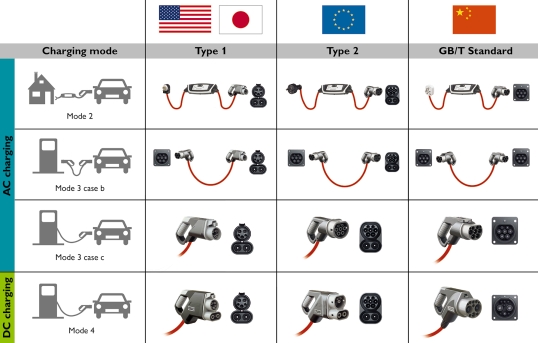
Power is transferred through a Type 2 connector (commonly called Mennekes due to the brand that lobbied to make it standard in Europe). This connector has five pins for three-phase up to 63A, although almost no one goes over 32A, and two signal pins for Proximity detection and Control Pilot.
![]()
Trivia: as I wrote earlier, Tesla uses the Pilot pin for single-wire CAN, but that's not the only non-standard way Tesla "hacked" this connector. They are also the only cars to use it for high speed DC charging, by supplying up to 500VDC using N and L3 for the positive terminal and L1 and L2 for the negative. This particular mode is initiated via CAN through a cryptographic exchange, to make sure no other car explodes by trying to charge at this non-standard station.
The PWM circuit
J1772 is a very old standard; unfortunately, while the industry could have gone with some nice bidirectional communication protocol like CAN, due to legacy compatibility we're stuck with this crappy PWM signalling method (there's a proposed Power Line Communication standard but no car implements it yet, and IMHO it adds unnecessary costs - I can add it later). How does it work?
It's very simple. Here's what happens:
![]()
- The EVSE outputs a +12V DC signal on the Pilot pin
- Inside a car there's a diode D1 and a resistor R2 creating a voltage divider with R1, that brings the Pilot voltage down to about 9V
- the EVSE measures the Pilot through R4, R5 and R6. These resistors translate the ±12V output to 0~3.3V signals for the microcontroller ADC. As soon as it reads 9V, the microcontroller starts generating a 1kHz PWM signal on the PILOT pin (via the CONTROL output).
- This PWM signal tells the car how much current she can draw. This can be a number from 6A to 80A. In the range from 6A to 51A, the value is calculated as DutyCycle = Ampere * 0.6
- The car perpares to charge; when she's ready, she closes the switch to parallel R3 to R2, bringing the high-side of the PWM signal to about +6V (the lower side still goes to -12V due to D1)
- The EVSE can now close the contactor and supply power to the car.
- If the car wants to stop charging, she just disconnects R3 and the EVSE will immediately disconnect the contactor.
![]()
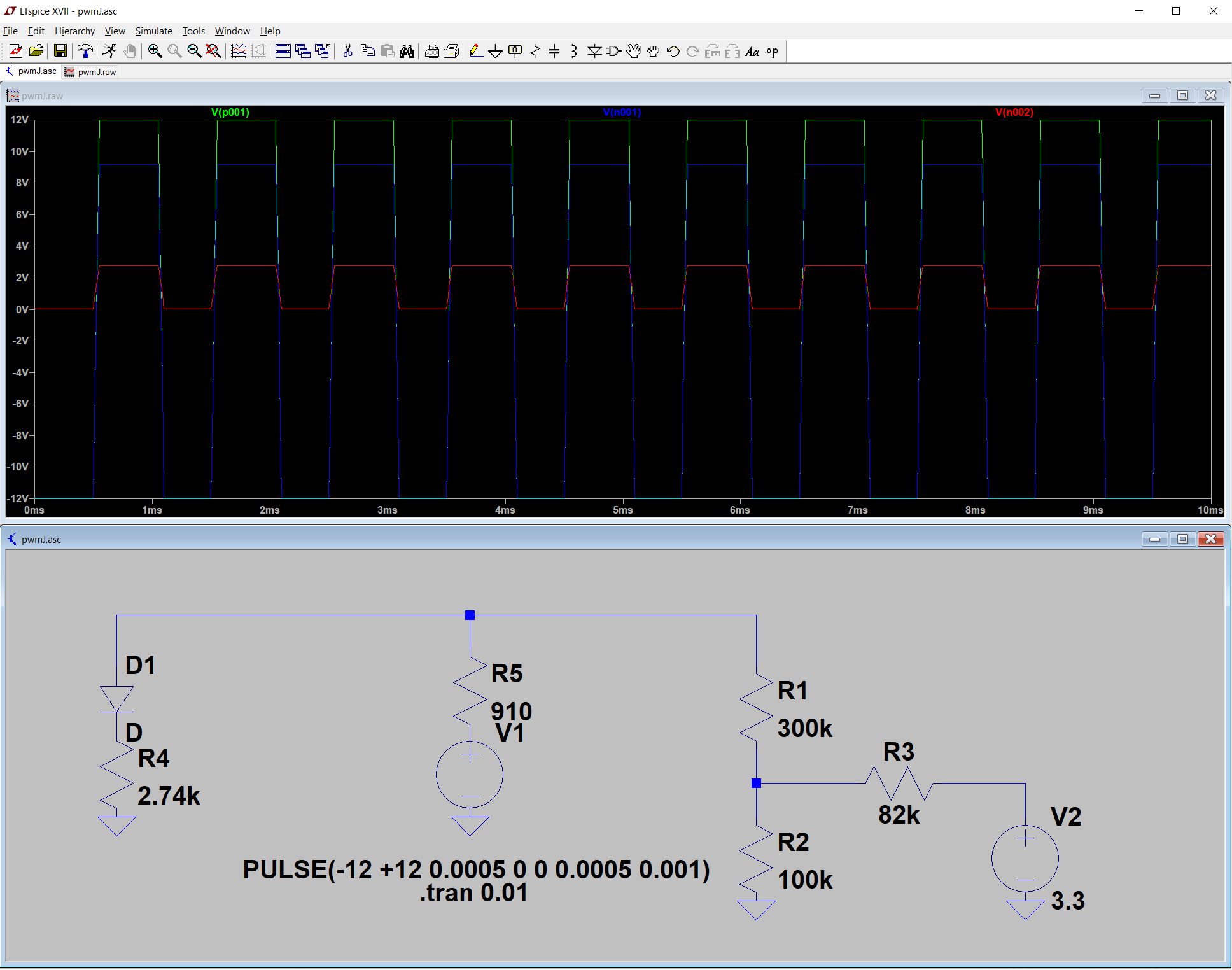
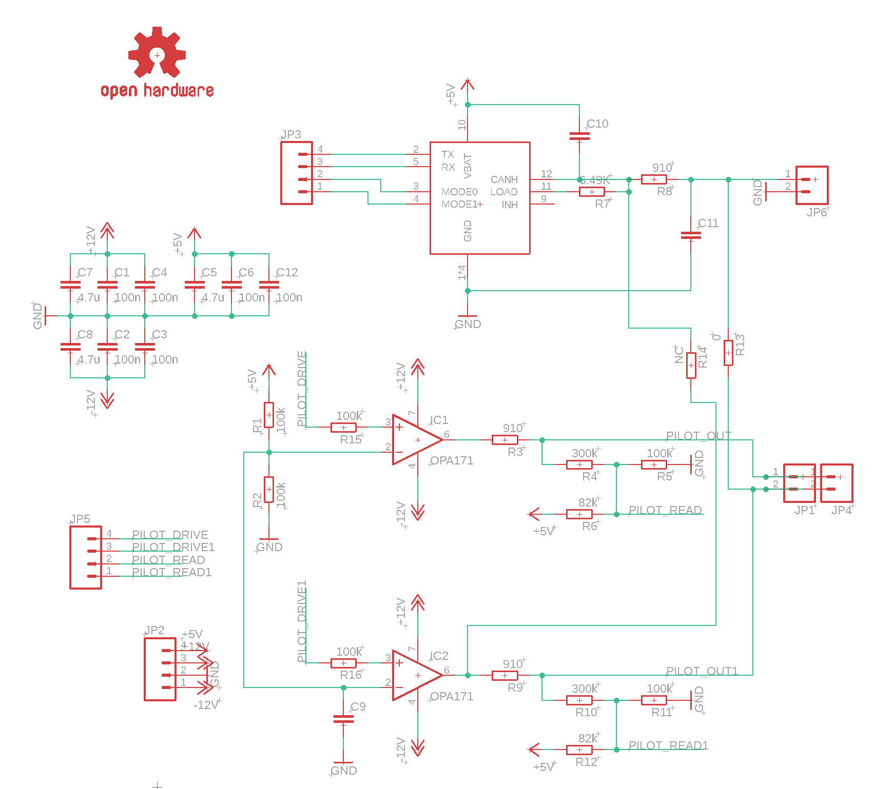
After calculating the resistors and simulating everything with LTspice, I designed a PCB to test various components. You can also find the NCV7356 test circuit in here if you want to test Tesla's one-wire CAN.
![]()
At the time, PCB makers were making great offers for 5x5cm PCBs so I split my test boards into smaller parts. This makes the design modular, and makes it easier to test single circuit blocks. Find schematics and PCB here!
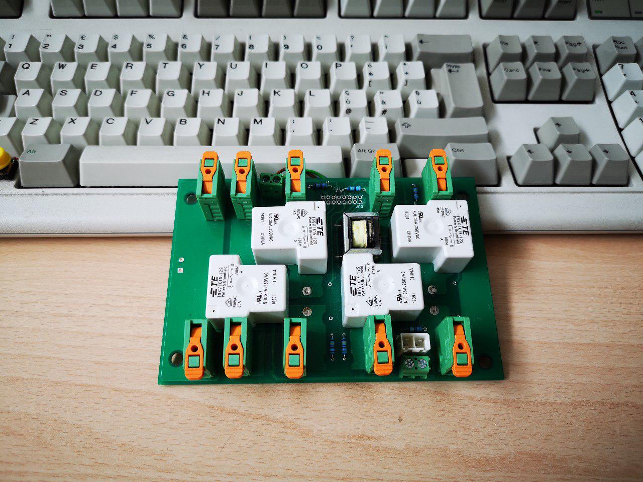
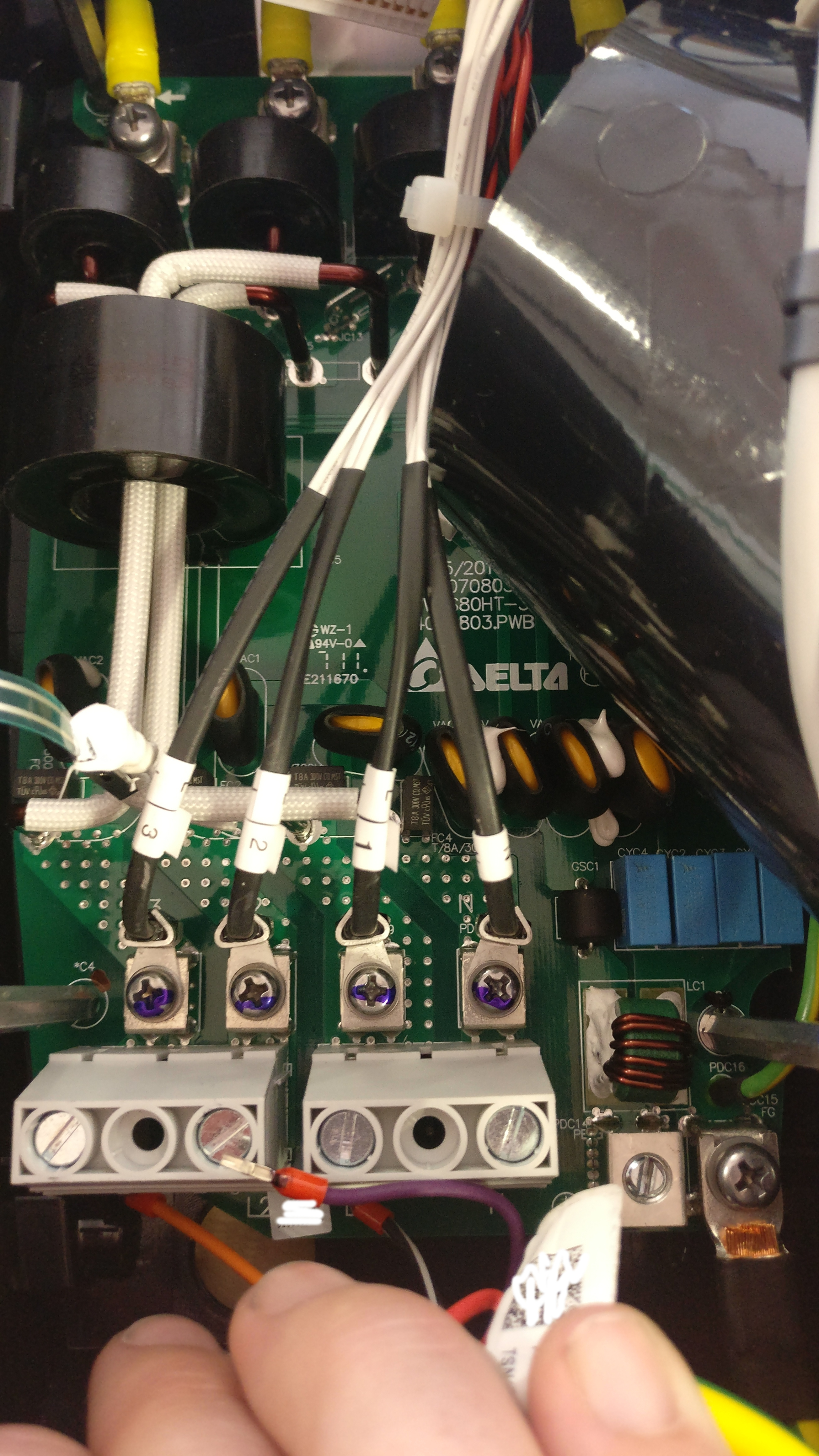
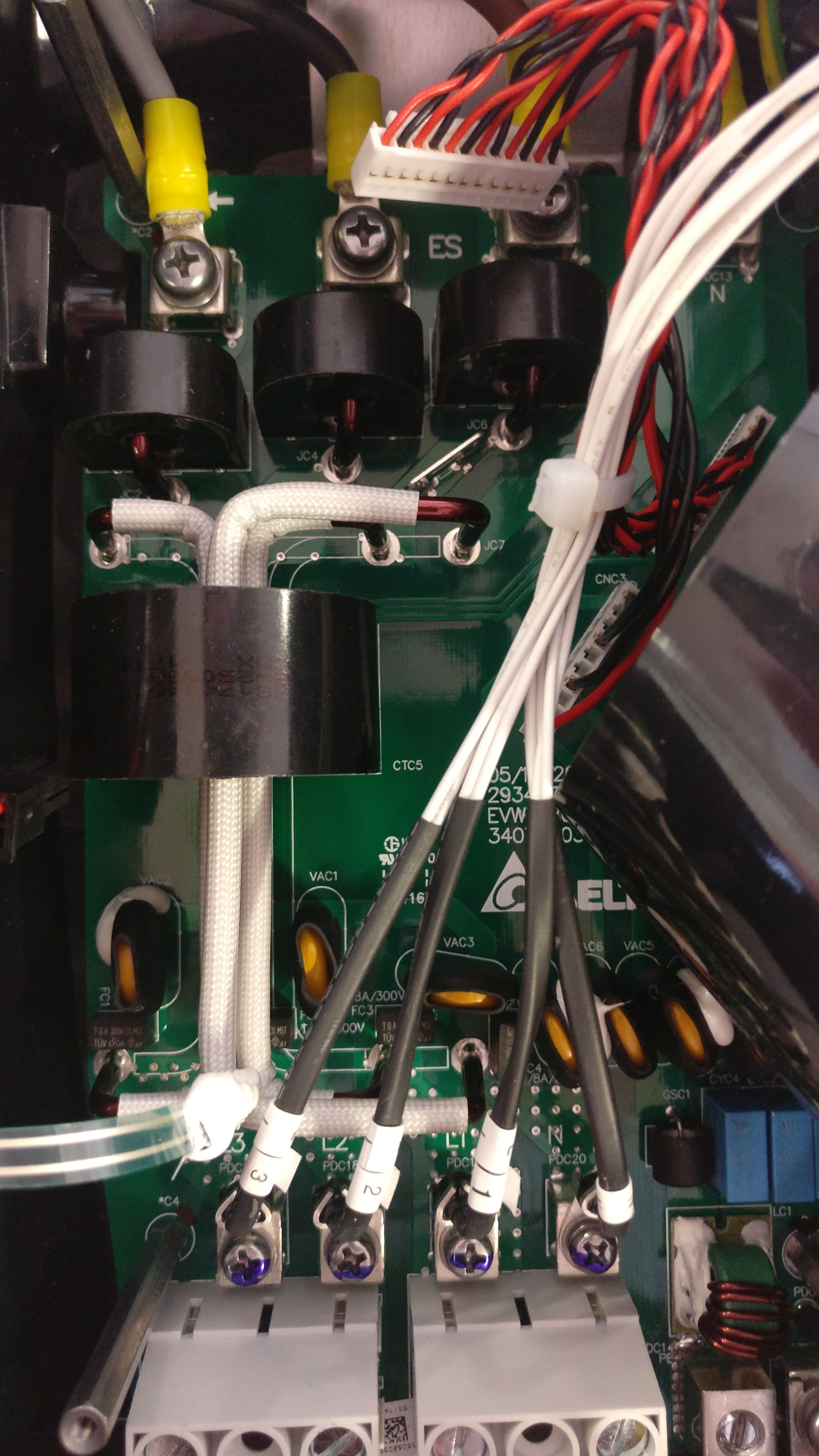
The power board
![]()
This board was built to test relays and current sensors. I designed it with generous tracks, mirrored on top and bottom, and ordered them with 2oz copper layers; I calculated a +10°C worst-case temperature rise with this configuration, and on my tests I measured a maximum of +4°C at full load, probably due to some air flow around my bench.
Relays are TE T9SV1K15 rated at 35A. There are pads for two types of current transformers: the CSE187L, rated at 30A, and the Pulse PB0027NL, rated at 35A. Both worked well; I prefer the Pulse transformer for its rating and smaller size, in SMD form.
Here I also added voltage dividers to measure input voltage, and to check presence of the output voltage to detect a stuck relay.
I designed a three-phase board and a single-phase one, but never tested the single-phase version. You can find both with schematics here.
Those two circuits controlled by a microcontroller would be enough to trick a car into charging. But that's just the basics. As we said earlier, we need to do much more to provide a safe environment for our users and comply with standards.
-
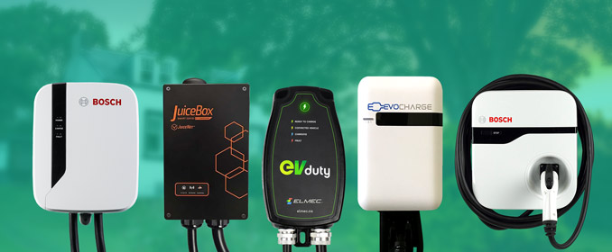
Design decisions and competition: Tesla, OpenEVSE, [redacted]
08/05/2019 at 09:04 • 3 commentsWhen building a product, it's important to study the other solutions available on the market, to learn from other's good ideas and mistakes. If you can't significantly improve existing designs, why bother?
OpenEVSE
![]()
This have been the obvious solution for hobbyist in the past. So of course I built one and was very happy with it! However, there are a few things I dislike about it:
- being designed for the USA market, it's only single-phase; there are a few workarounds to make it 3-phase, but there are many drawbacks
- the standard box they offer has a very plain look, and the 16x2 display is so 90's
- it only connects to WiFi, via an ESP8266 - no ethernet and less easy to program if you're not familiar with the platform.
I liked their pilot signal circuit, so I implemented it in my design. More about that later.
[redacted]
![]()
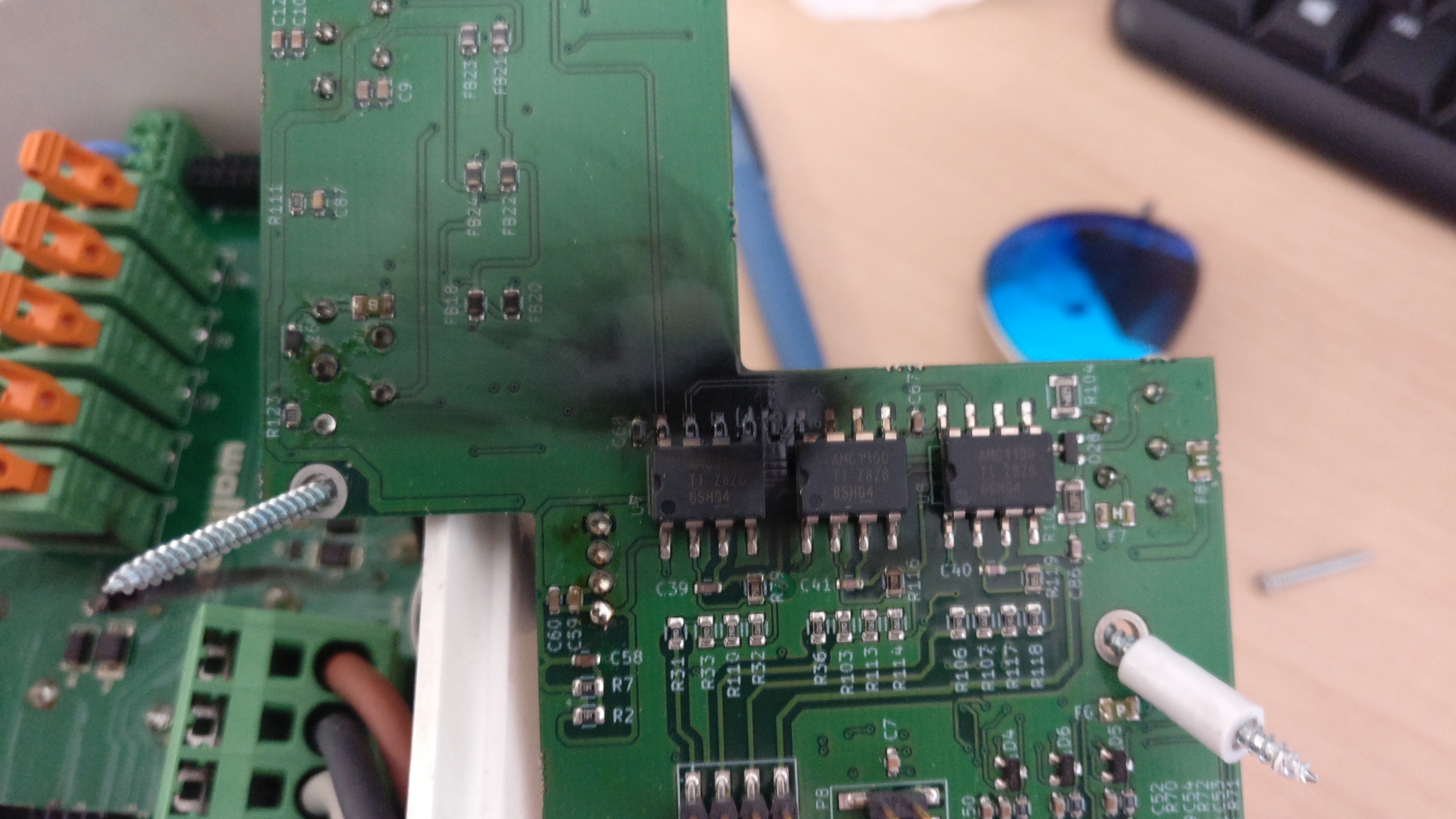
Looking for a nicer (and 3-phase) wallbox to install at the office, I stumbled upon [redacted]. This company makes beautiful products, with some nice features, but I'm now super pissed at them.
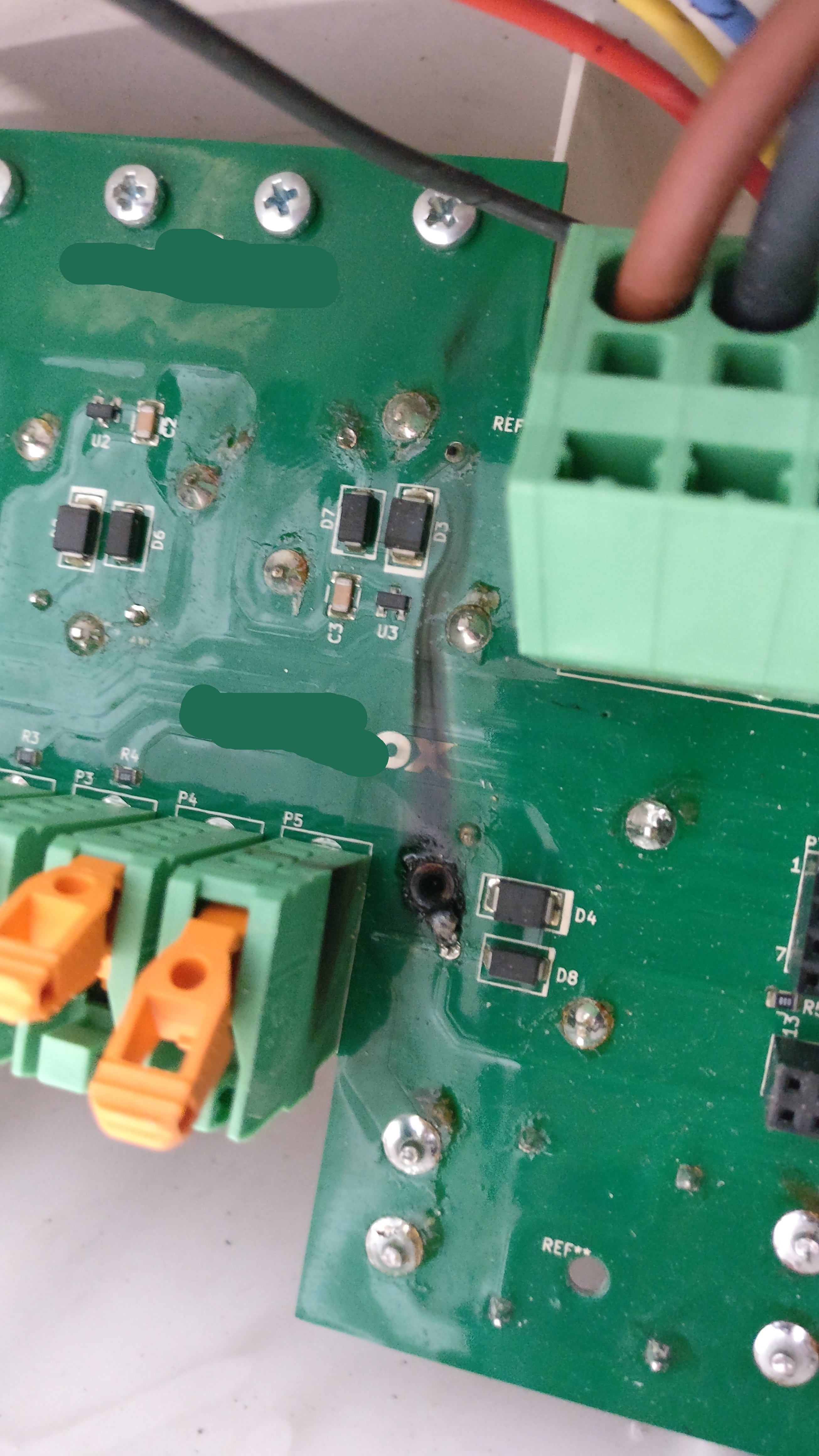
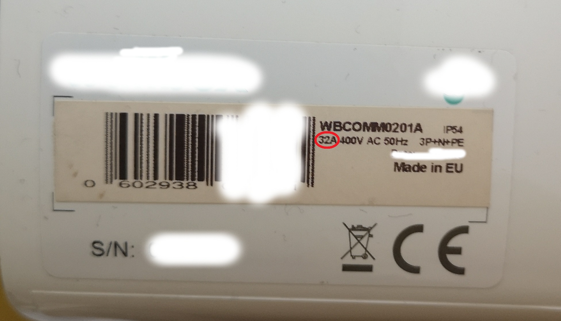
I used this wallbox for a while, until... it exploded. I should have really followed Dave Jones advice here, because if I had tore it apart before turning it on I would have noticed that these f***ers used 30A rated components for their 32A rated product. I have no idea how they passed certification.
So this ticking bomb heated up until THE SOLDER ON A RELAY PIN MELTED and shorted another terminal below. Luckily, this triggered the main breaker, but the charger could have caught fire causing a sh*tload of damages.
![]() Black Smoke Of Death; this is the upper board that received indirect damage
Black Smoke Of Death; this is the upper board that received indirect damage![]() Must have been hot in here
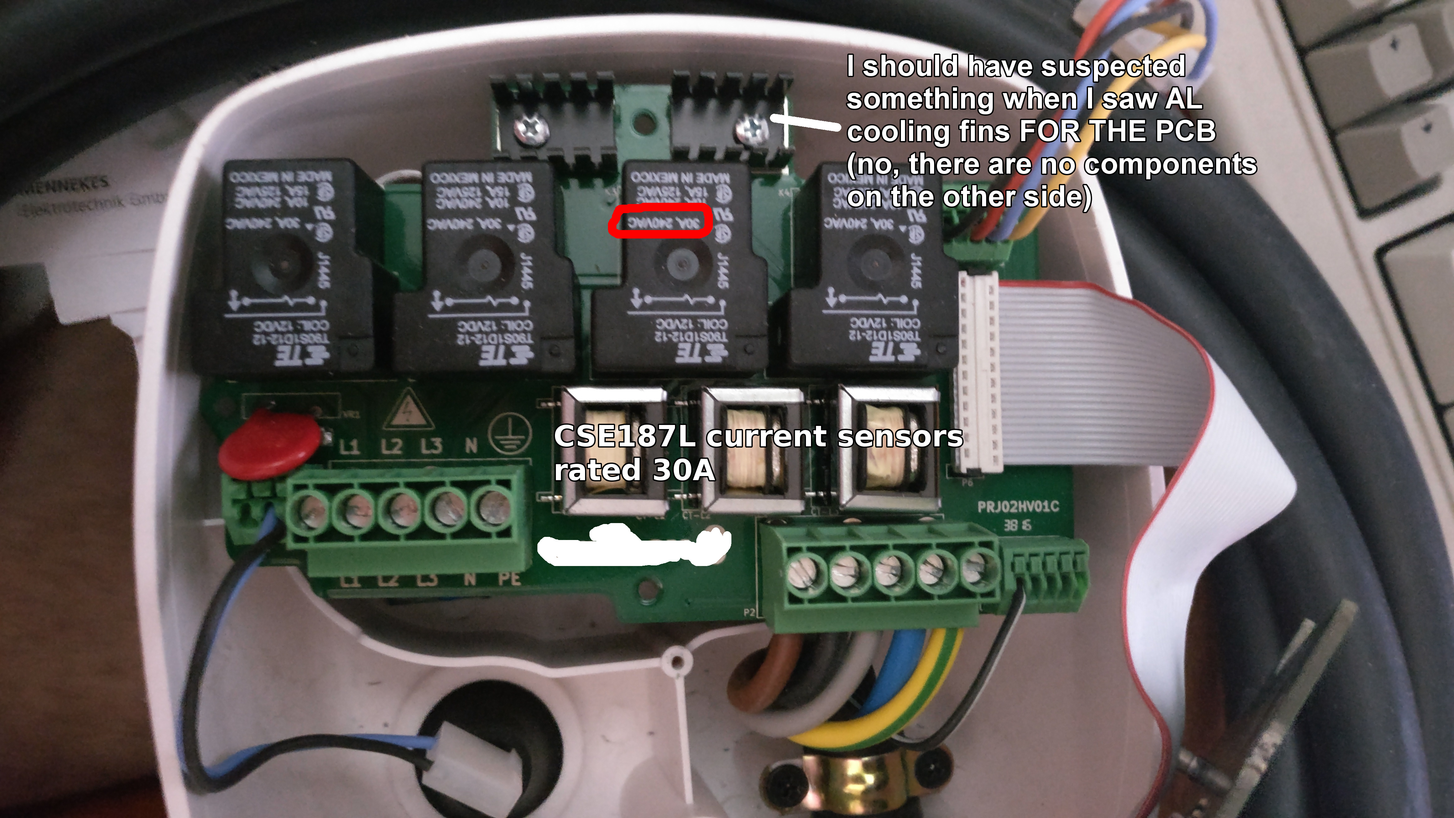
Must have been hot in here![]() Who rated this 32A?
Who rated this 32A?![]() SERIOUSLY??
SERIOUSLY??Their new product still uses these kind of relays, but to be fair there now is a 40A version in the same format so I guess (hope) they're using those. I didn't have a chance to disassemble one yet. Their current sensors should still be rated at 30A AFAIK, but that is a linearity rating; the copper should be big enough for more, only the measurement linearity would be worse - easily fixed in software.
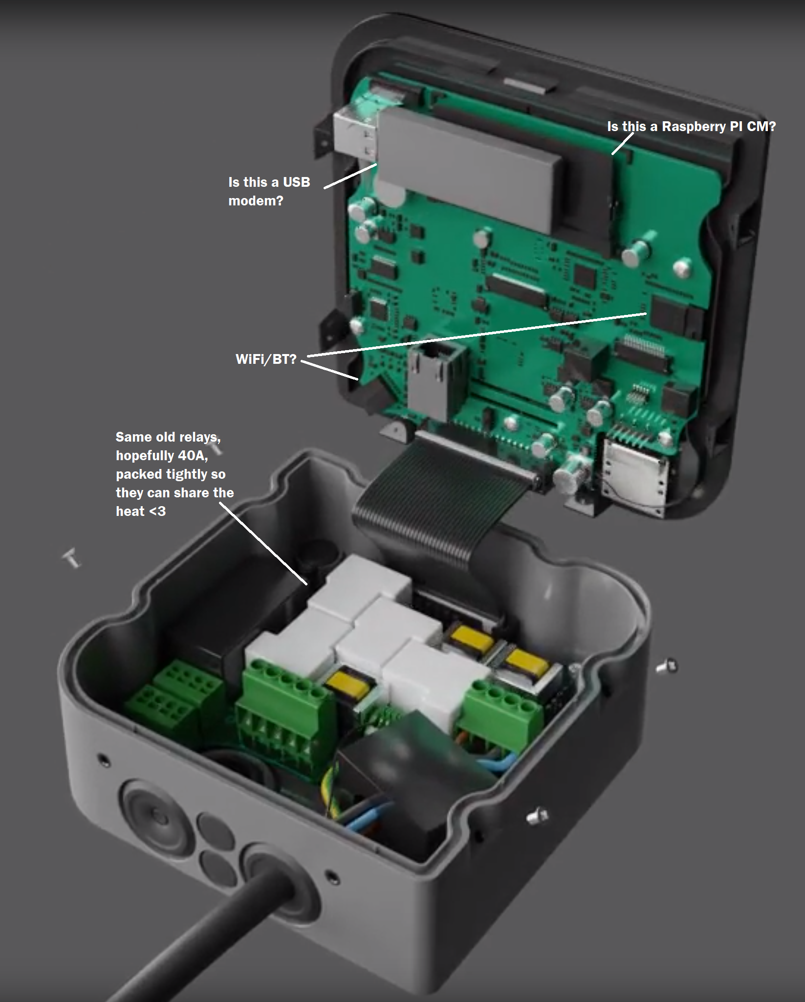
![]() It IS gorgeous. I love their new design.
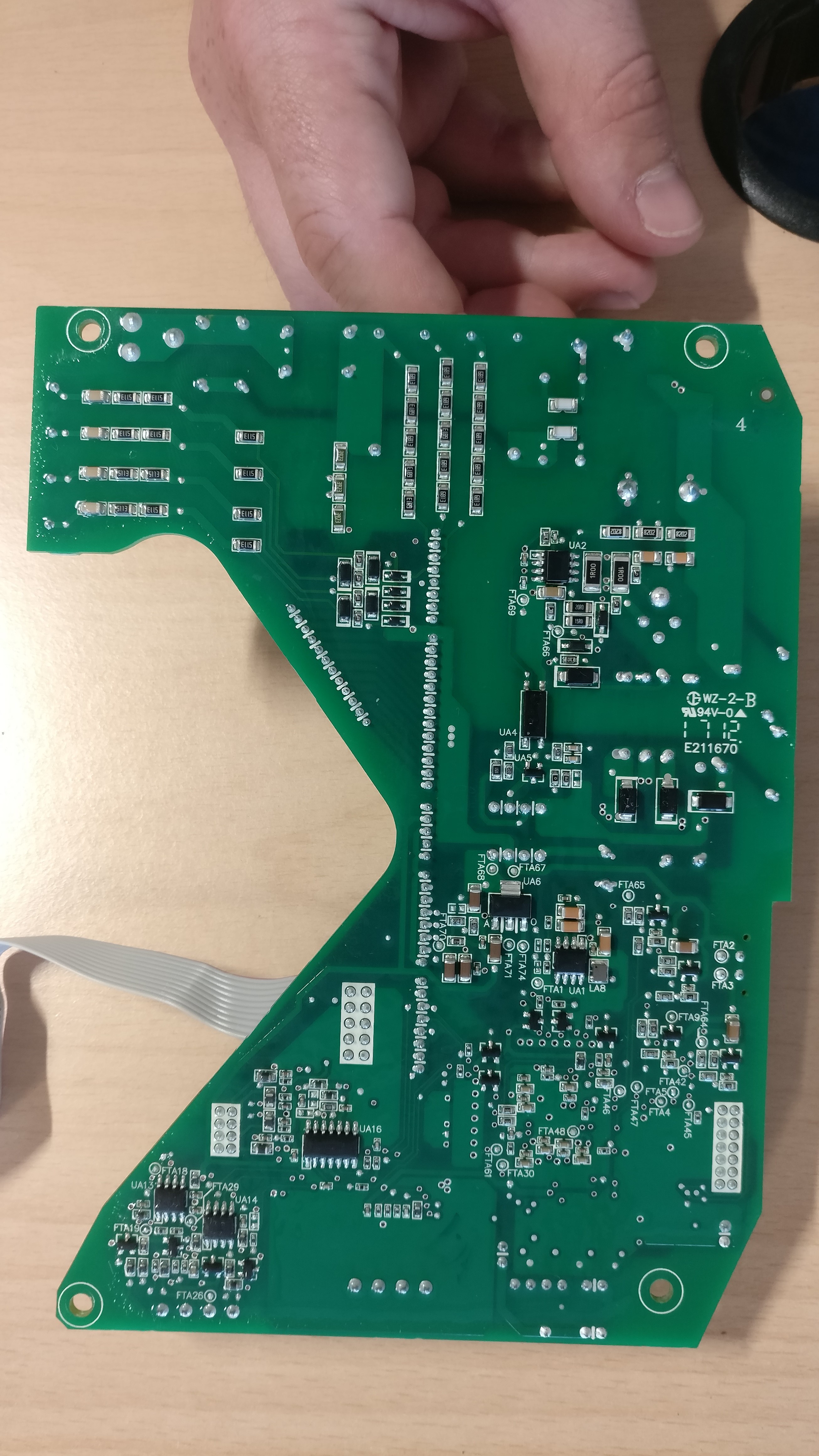
It IS gorgeous. I love their new design.At around the same time I was experimenting with a first prototype of my own design, with the 35A version of the same relays.
![]() One of my first prototypes
One of my first prototypesThis made me reconsider my choices and look around for better solutions, so I disassembled...
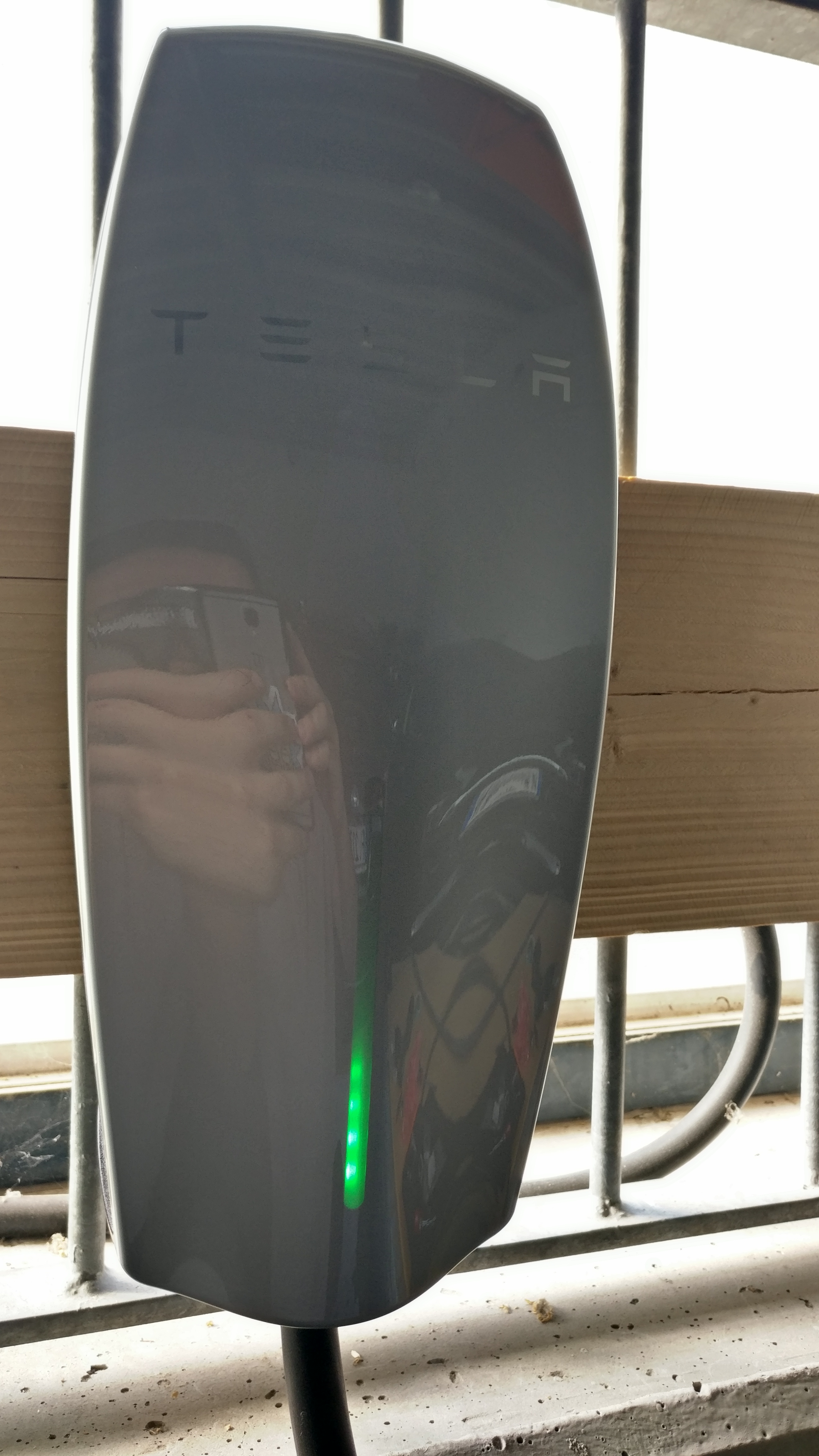
...The Tesla HPWC
![]()
This wallbox is what I'd consider state of the art. It is so over-engineered that I'm sure the guys responsible for it are sleeping like koalas. That's the feeling I desire; I want to sleep well knowing that I didn't cut any corner and that if I get a call from a customer with a burned-down garage I would know it wasn't my product's fault.
Here, enjoy some pornography:
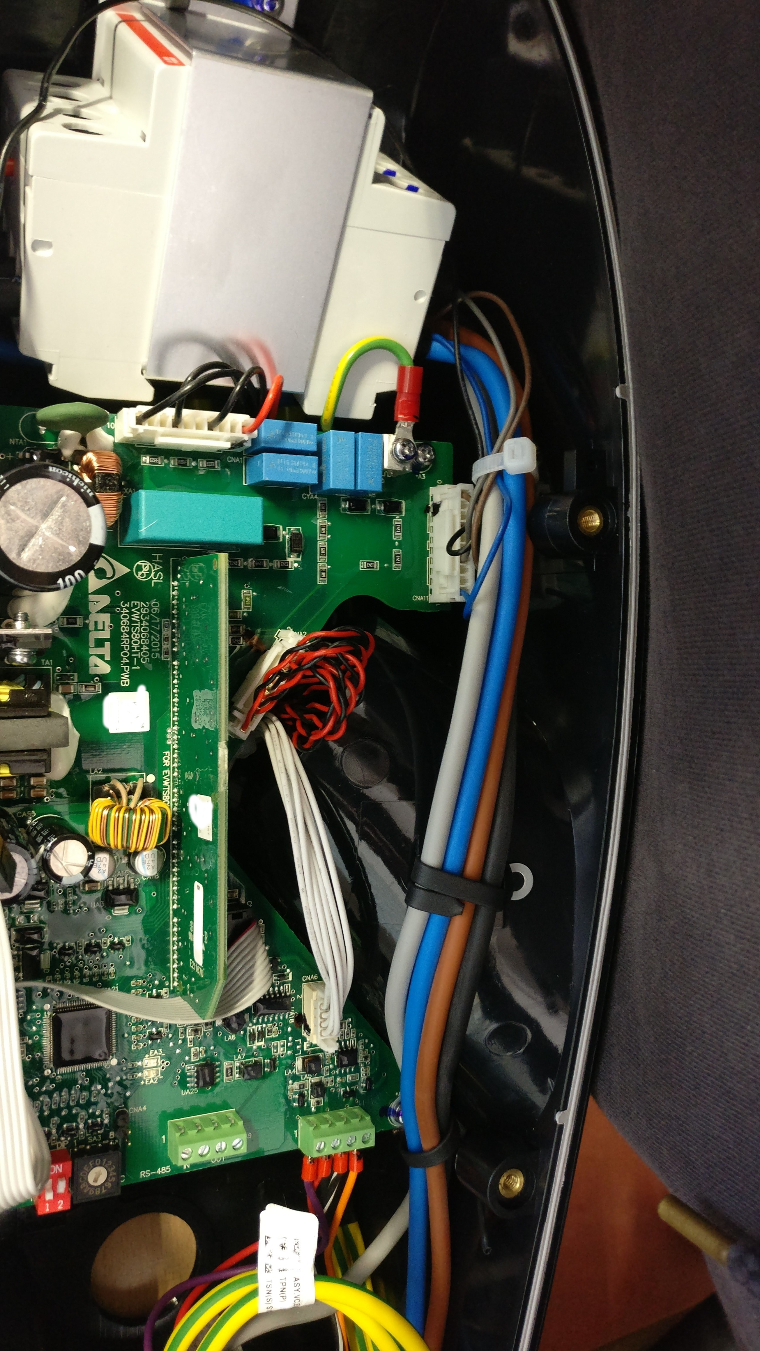
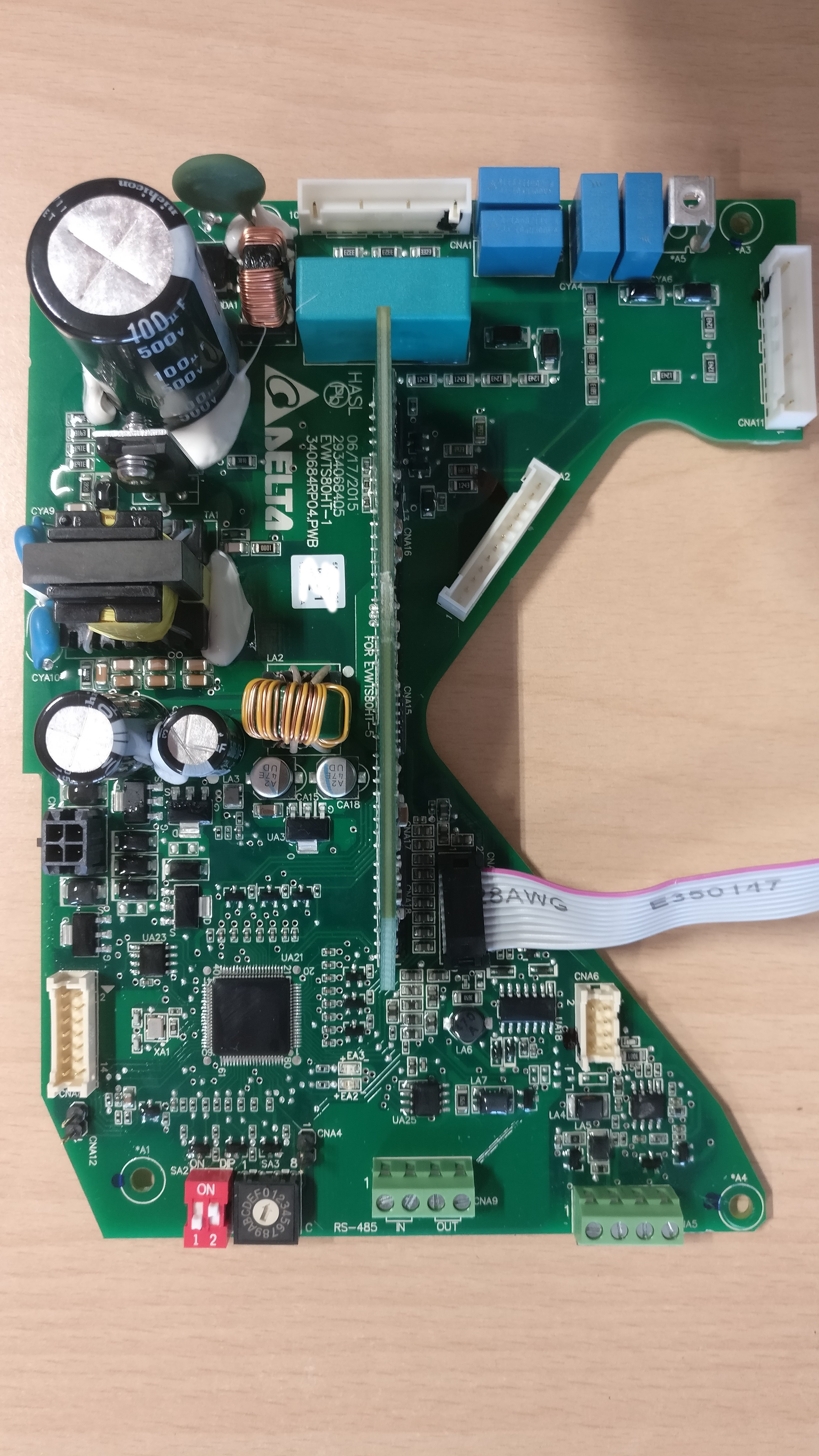
![]() Look at that HUUUGE contactor!
Look at that HUUUGE contactor!![]() It's all run by a TI DSP
It's all run by a TI DSP![]() Look at those nice voltage dividers with a bunch of resistors in series to increase isolation!
Look at those nice voltage dividers with a bunch of resistors in series to increase isolation!![]() What are these? Temperature sensors on each line? Am I dreaming?
What are these? Temperature sensors on each line? Am I dreaming?To be fair, the temperature sensors are probably needed because the final installer will have to tighten these screw terminals, and they don't always do the best job. Spring terminals would work way better here. More on that later.
![]() Those copper wires certainly look THICCCCCC
Those copper wires certainly look THICCCCCCTo be fair, Tesla's HPWC (High Power Wall Charger) isn't perfect either; you can buy it only if you own a Tesla, and it's not "IoT". It has RS485 though and the protocol has been reverse engineered, a guy even fitted a Raspberry Pi Zero inside it, so if you're crafty and curious you can mod it.
Bonus Trivia: as you may already know, Teslas are "computers on wheels", always connected and receiving constant updates. This philosophy seem to be missing from the HPWC, as it looks like there's no way to upgrade its firmware. But Tesla is also famous for thinking outside the box: turns out, every Tesla car hosts a copy of the latest HPWC firmware and updates them when you plug in to charge. They do so by starting a non-standard single wire CAN communication on the Pilot pin, the same way they talk with Superchargers, via a NCV7356.
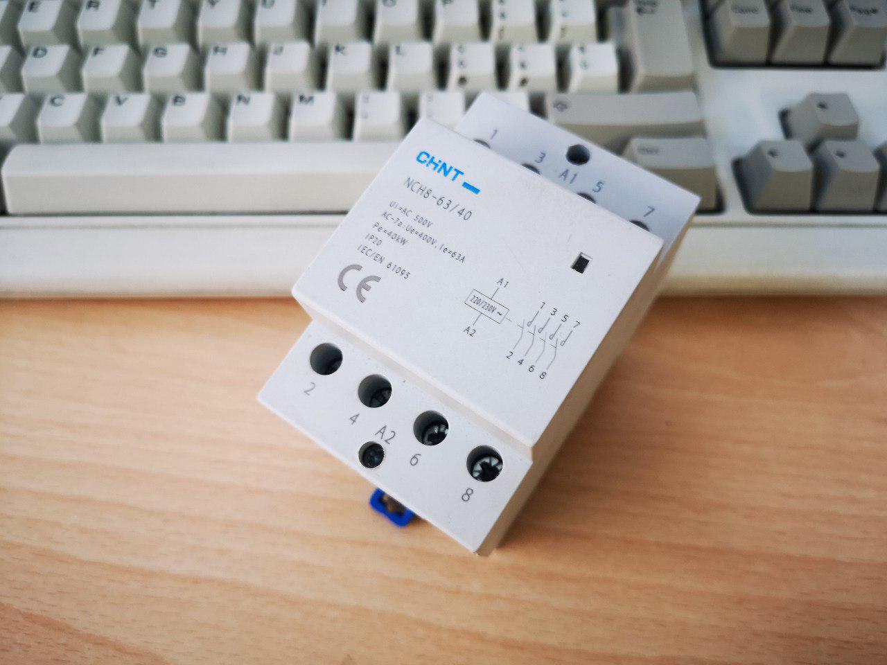
But the greatest tip I got from this teardown is that, really, the best way to switch a 32A constant load is to use a proper industrial contactor. Unfortunately, the ABB model Tesla's using is really expensive, way out of our startup quantity price range. But there are many companies making industrial components, and one day, when power went out at my home, I found the answer:
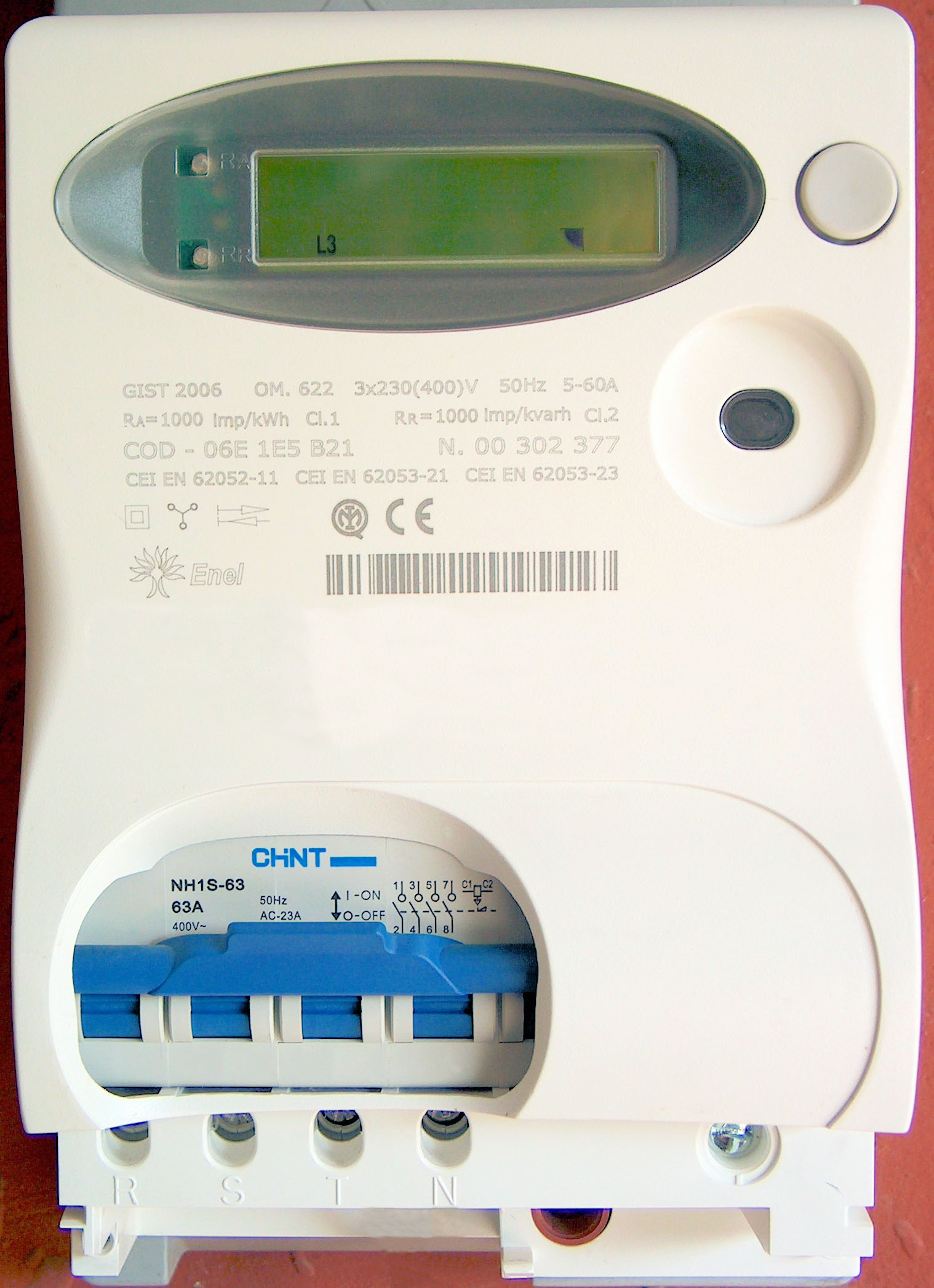
![]() ENEL, the Italian energy distributor, uses CHINT components in their million meters installed all around the country! This means that they're cheap, and they work well! And presto, I contacted the local distributor and found the perfect device:
ENEL, the Italian energy distributor, uses CHINT components in their million meters installed all around the country! This means that they're cheap, and they work well! And presto, I contacted the local distributor and found the perfect device:![]() Certified in Europe and guaranteed for 63A, almost double what it will ever see, with a sturdy industrial case and a price point that makes it worth it, despite costing about four times more than the relay solution.
Certified in Europe and guaranteed for 63A, almost double what it will ever see, with a sturdy industrial case and a price point that makes it worth it, despite costing about four times more than the relay solution.But I'm getting ahead of the story here; there's still a lot of history to tell that happened before I found this contactor! Stay tuned!
-
EV charging basics
08/01/2019 at 10:16 • 0 comments![image stolen from Phoenix contact]()
Before going any further, there are some basic details you should know. Note that I'm writing about Europe, other regions may differ slightly.
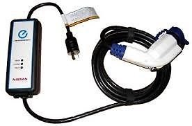
The "easiest" way to charge an EV is in Mode 2: here you have a special cable that you can plug to any AC outlet and to your car. This usually allows charging at 3kW, or roughly 10km/h and should not be used regularly.
![]()
On the cable, near the AC plug, there's a device called EVSE. This guy has a few functions, according to the IEC 62196 and J1772 standards:
- it makes sure that a car is connected before closing the relays to power the plug. This is important because plug terminals are quite easy to touch with a piece of metal
- it checks that the relays don't get stuck
- it detects AC residual current to detect Ground faults
- it tells the car how much current it can draw (usually limited by wire section - but it doesn't know how thick are your house's wires)
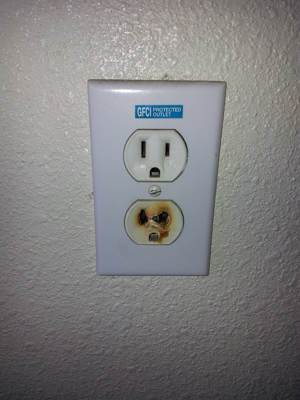
This is not an optimal solution as you may imagine, as house plugs are usually not designed for a constant and very high load, so browsing EV owners forum you can find a lot of burned plugs images:
![]()
To avoid this, to enable charging at faster rates and to improve safety, at home we usually install a Mode 3 charging station, commonly referred to as "wallbox".
![this photo was stolen from the web too]()
Wallboxes are just more sturdy EVSEs that are stuck to your wall and connect directly to the mains wiring, through the usual breakers and RCD/GFCIs. Now you can charge up to 22kW (~100km/h) in complete safety!
You can also choose if you want it with a socket (and you'll have to bring your own male-female cable to connect the car) or you want a dangling cable with a plug. I prefer the second option as it's much easier and faster.
If you're curious and want to know more technical details, check out OpenEVSE's theory of operation here.


 This seemed a great idea at first, but it became soon clear that all of these complications would come back to bite our asses in production. So we made the sensible choice and ditched the infinite mirror idea altogether, simplifying the design by placing all the components upright as they were meant to be. Here I'm testing the new possible layout:
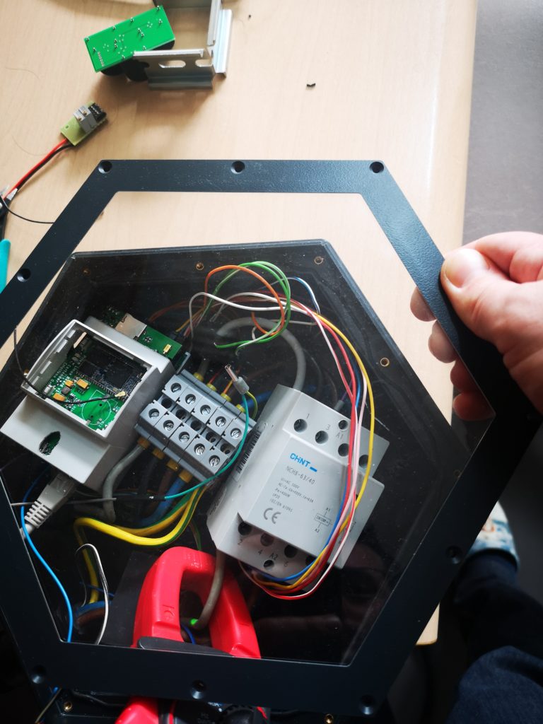

 Unfortunately there are big drawbacks for this solution too. The back plate would be separated from the wall, but that can easily be solved with a machined (expensive) plate or some pressure-formed dimples if made with sheet steel. We were also worried about bad alignment of the two parts making an ugly visible seam. Despite the cheap extrusion, this method would require a lot of additional parts and machining, increasing the cost too much.
 It's impressive the amount of detail you can get with this metal. We worked with the company to get our design made, but after working on the model they couldn't find an easy and cheap way to make the mold without introducing ugly artifacts from the injection points in user-visible areas. It's also not a great idea to build high voltage stuff inside a metal case, despite the good grounding and isolation. But my adventures with Zama are definitely not over, I'll find a way to use this material in a future project!
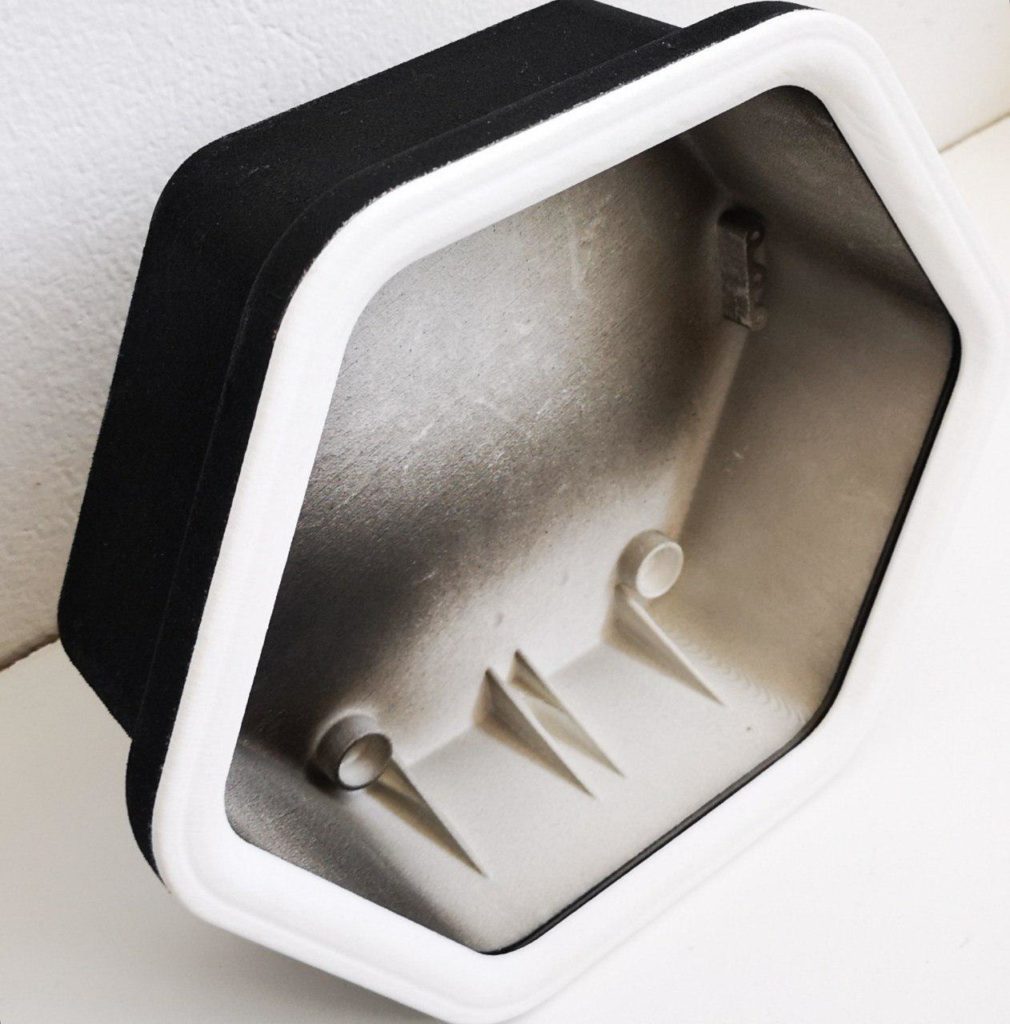
 Enjoy my updated