Close
0%
0%

Optical scanning microscope

How to scan very small electronic circuits like displays.

Public Chat
Similar projects worth following
I was interrested in microscopic electronic, like display drive circuits and integrated circuits.

One day I was playing with my phone, and a drop of water landed on my screen. That little water drop formed a little microscope, so I coud see my phone screen pixels. That water started this project, because after that I wanted to look more and more smaller object on it. I decided, I want to photograph what see on that screen. 

I work in the display industry, but I never saw with my own eyes how a screen really works. I was interrested about the electrical side of a screen, like how they could operate that much pixels in the size like phone.

Because of my work I saw some thin firm transistors on a layer of screens, and also a bit of research I knew what to look for. 

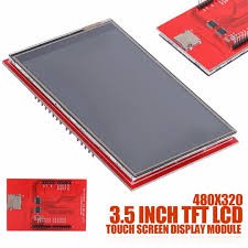
I was thinking about how to make a cheap big magnification microscope. It was not easy, but I rememberred the CD readers head has a really good optic in it. I started playing with my Iphone screen and a cd reader head, I could saw much more details then before, but that was not enough form me then. After I tried with the same optic with my Iphone 7 plus camera so I started photograph. I had a cheap chines LCD touch screen for an arduino uno what I never used for any project, so I made a sacrifice. I used the cheap screen back light to light the screen then placed the microscope optic, but the result was not the best. I only could see the red, green and blue pixels, nothing else. 
After a lot of struggle, I found out the screens usualy built from two glas layer between the liquid crystals. The top glass has black masking where they want to hide the controll circuit. That mean between two sub-pixel it is black area. The problem with this the transistors and the controll lines are between these pixels, so I could not saw them. 

Then I disassembled the screen and removed the front LED backlight and all the polarizer films from the front and the back also.

With this I coud see the transistors and the lines from the back side, but the problem was still that black masking around the pixels I tried to see from the top.

I had no chance and had to try separate the top and the bottom glass layer. It was feirly easy with a sharp blade.

Then lets see what cold I achieve with this:
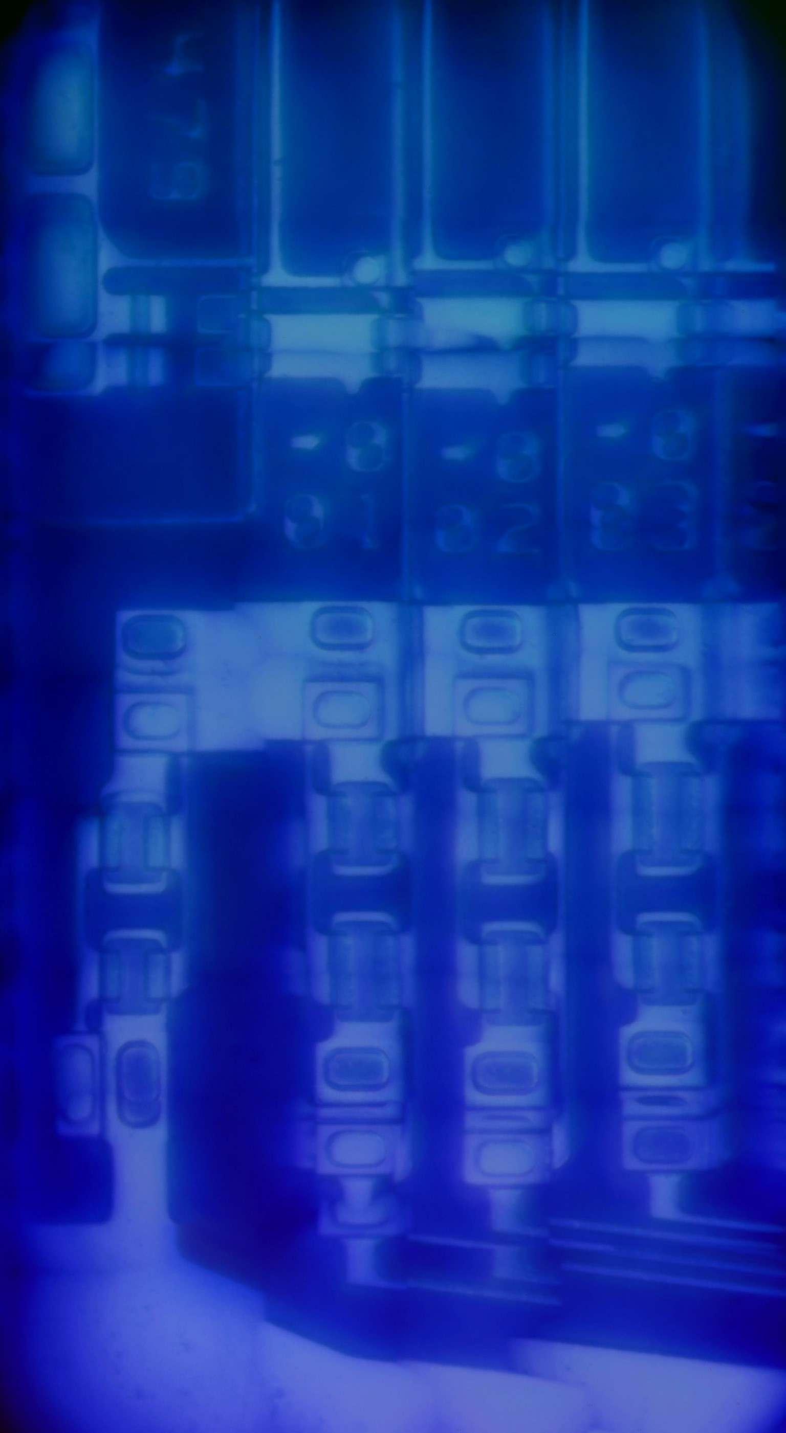
 Not so bad right? I achived this with a CD reader head optic a RGB led and my phone camera.

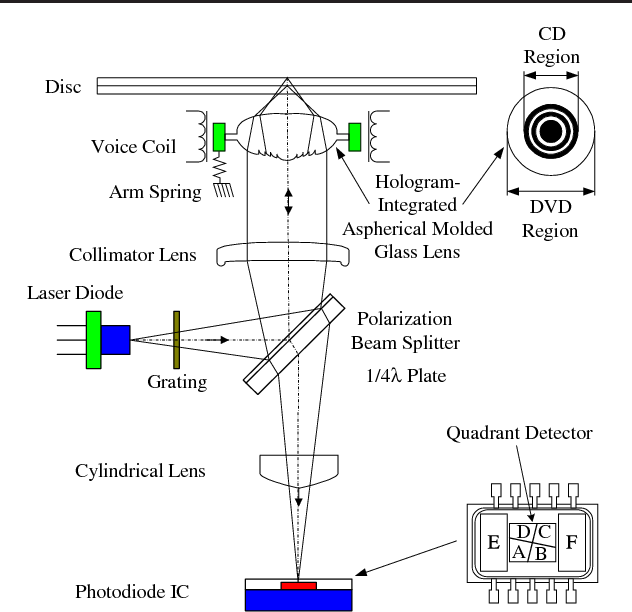
The CD reader head has a good option because it is reflective optic, so it usually has a laser what is shining down to the surface then the light comes back to a photo transistor, and that how it detect data on CD surface. This point I replaced the laser with a RGB led and I removed the photo transistor also and ther went my phone camera. 
This picture was created from several picture combination, that why it is not perfect.

Then I decided to improve the system by adding X - Y movement too, so I could search for interresting parts.

I had an old pen plotter what long time I was looking for where can I use it.
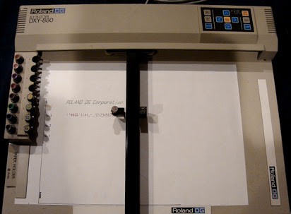
I modified the controll electronic with a modern arduino CNC shield, so then I can write software for it.

Also needed USB camera instead of my phone camera, so I was looking for a cheap solution and I found a usb microscope camera, I knew it is not so great, but it has magnification already and I did not needed big resolution, you will understand it later why.
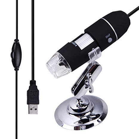
 I was learning Python OpenCV  for a couple mounth so I know I will capable of controll everything from python. I wrote a little code for move the X - Y movement like a scanner head, then I took pictures with the USB microscope and converted it to gray and added it them, so then I finally could take high resolution photos like below.

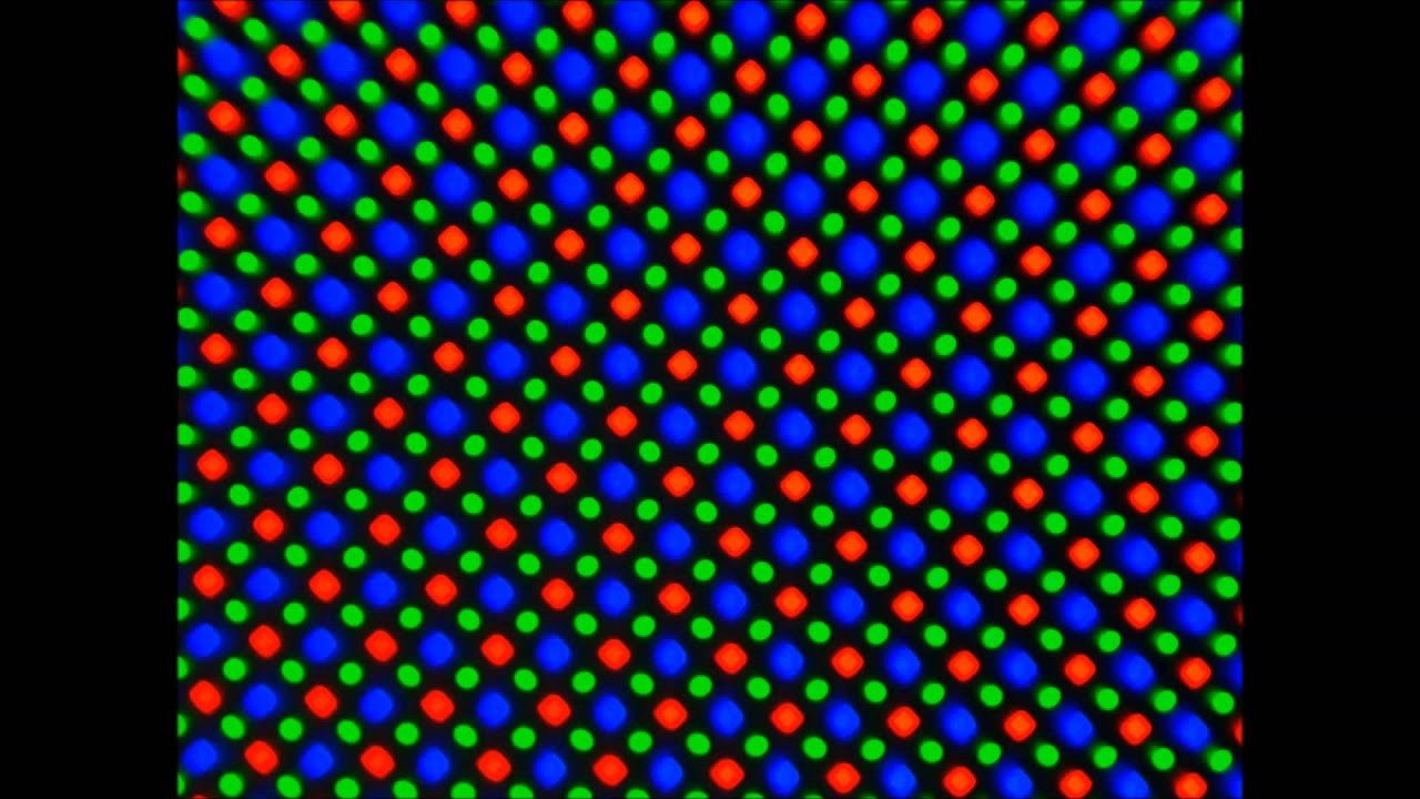
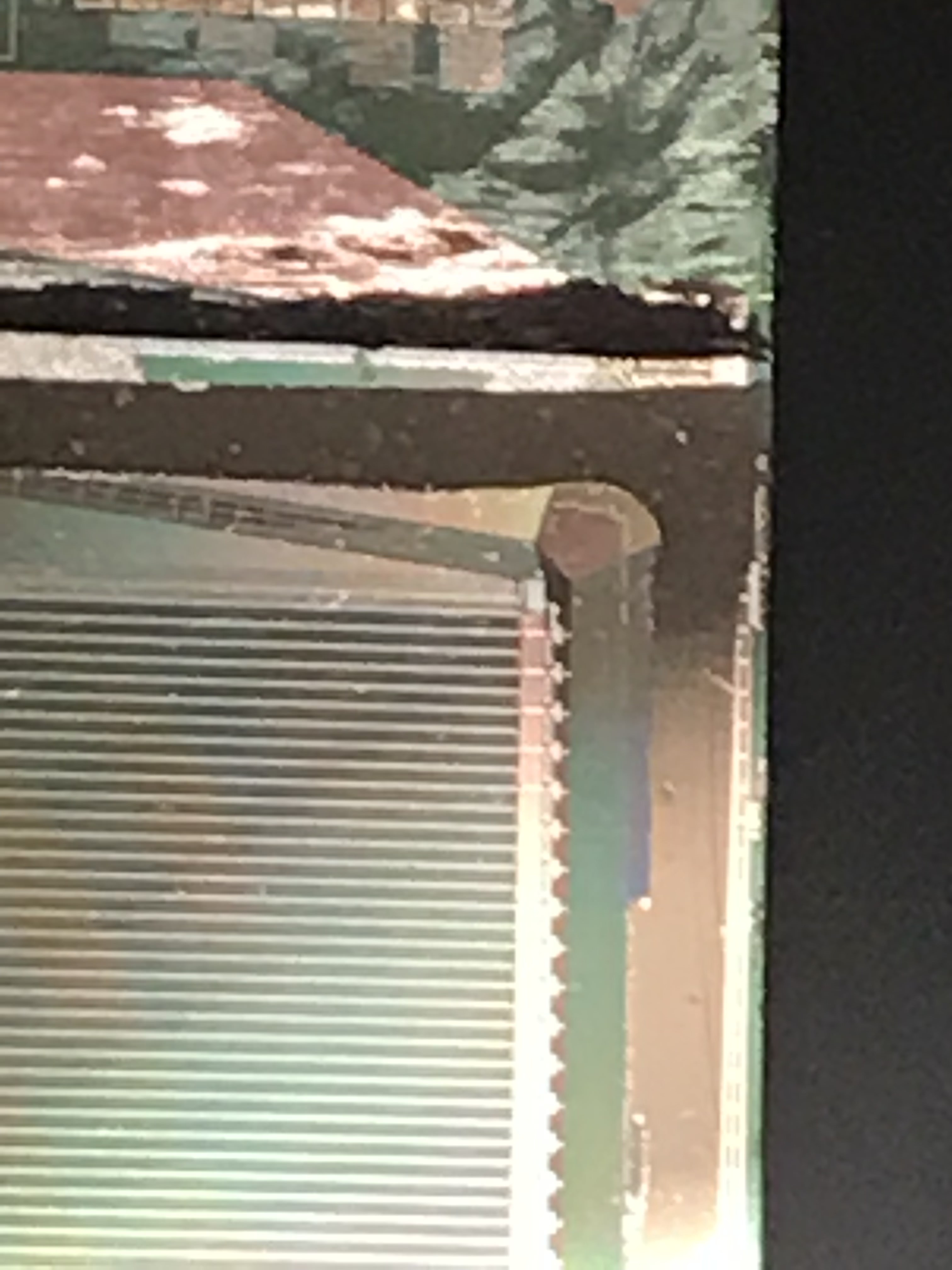
First show the display under 10X magnification from my Iphone camera, so you can compare how small these thing actually: (sorry for the bad focus, under this much magnification the phone could not focus very well)
And the scanned image under the microscope: (stiched together by python about ~200 picture)
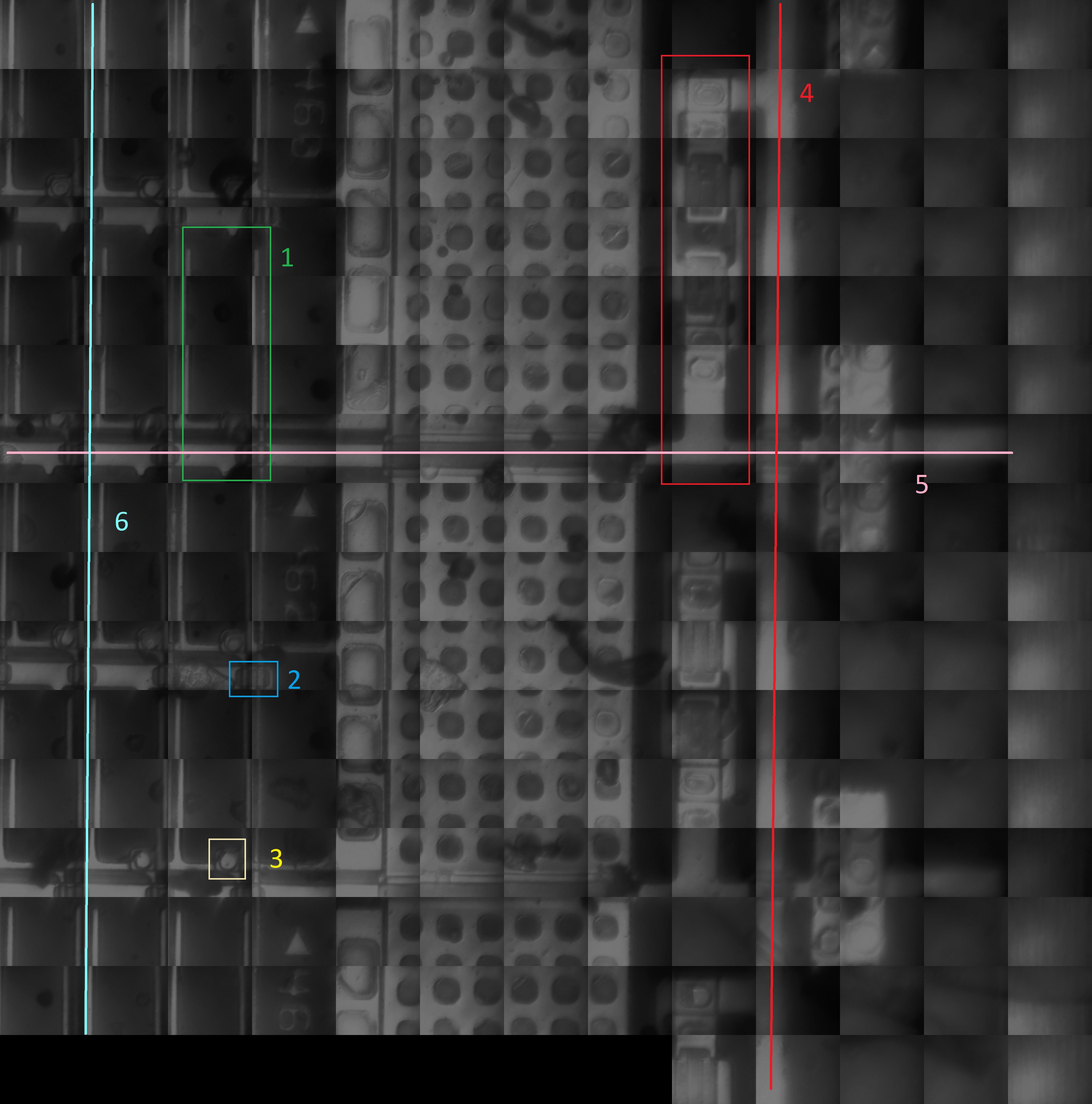
 It is not so beautiful, but can be seen what needed. ...

Read more »
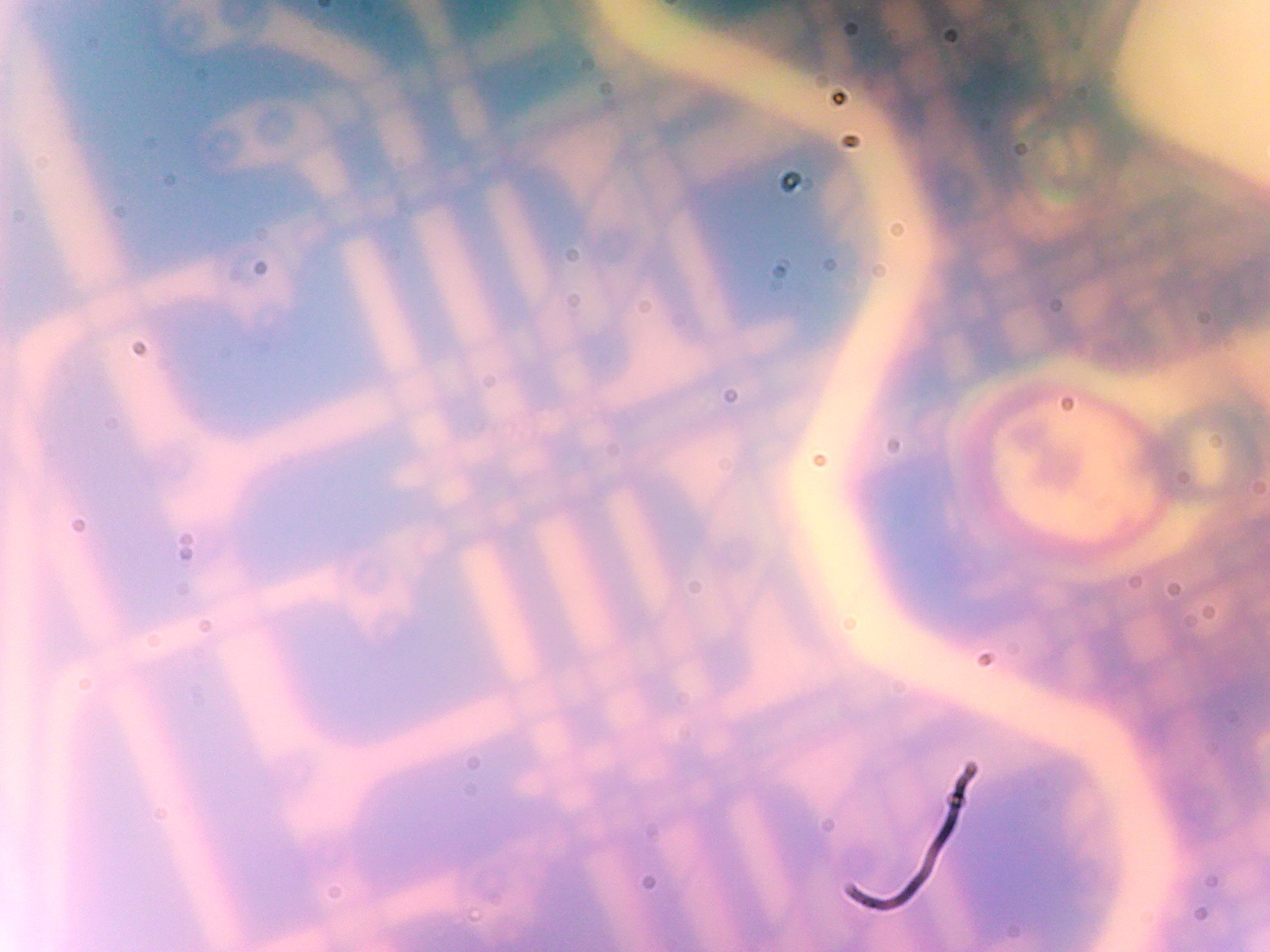
arraymatrix98.png

Samsung S8 display array

Portable Network Graphics (PNG) - 24.93 MB - 10/22/2019 at 20:15

Preview

arraymatrix4.jpg

Samsung S8 display array curve

JPEG Image - 8.43 MB - 10/22/2019 at 20:14

Preview

arraymatrix12.png

TFT array photo

Portable Network Graphics (PNG) - 7.95 MB - 08/04/2019 at 18:36

Preview

  • Microscope upgrade

    Máté Tóth04/25/2020 at 15:20 0 comments

    Hardware modification

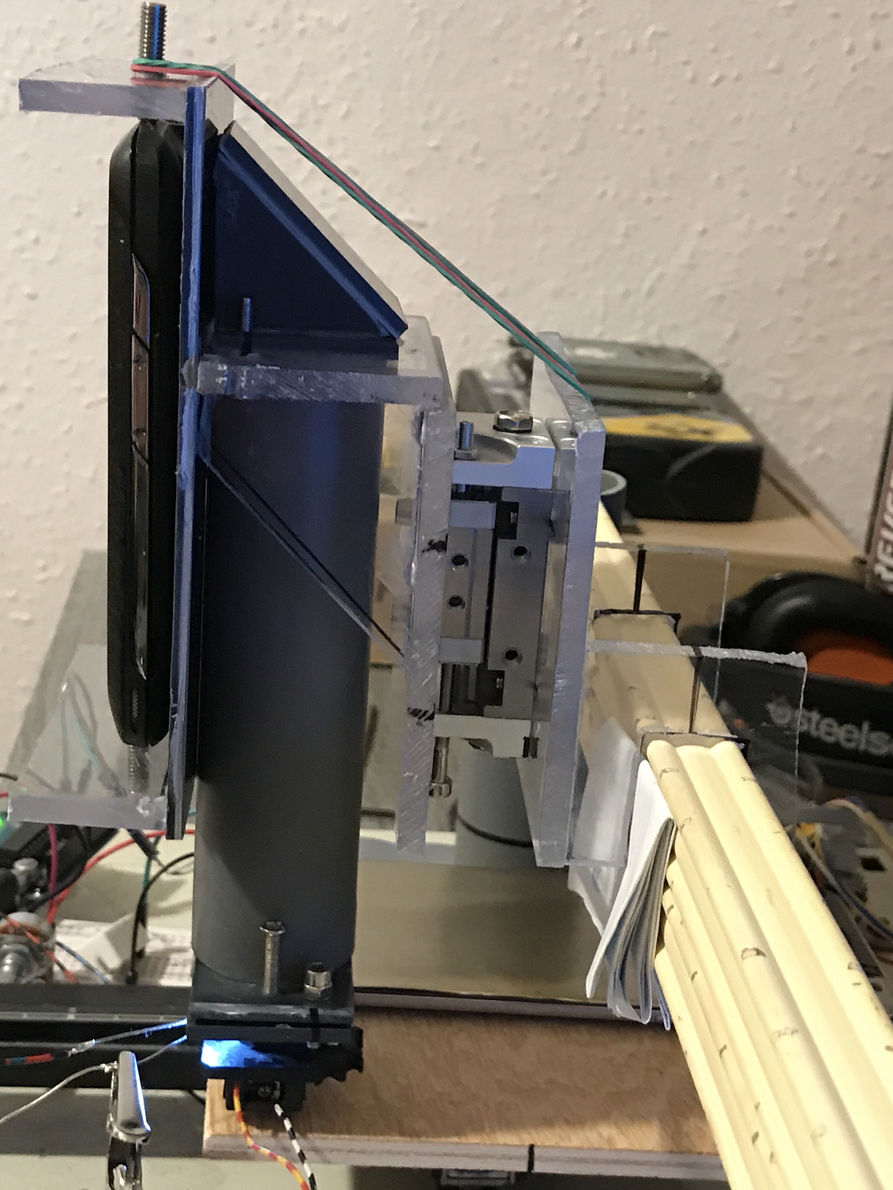
    I wanted more colorful and better scanning results, so I decided to make some upgrades on the microscope. I needed more flexibility on the alignment setup, and some structural rigidity for less shakiness. 

    I am not a mechanical engineer and I think everyone see how did it go...

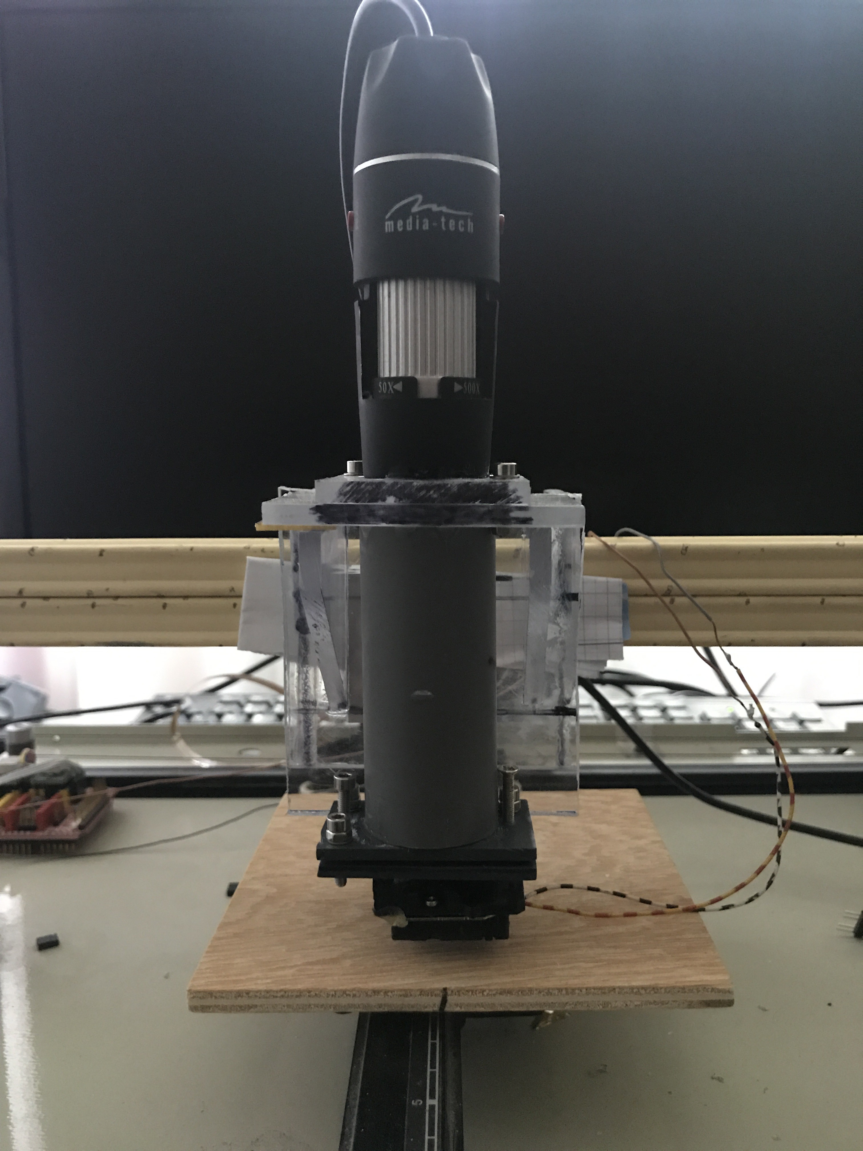
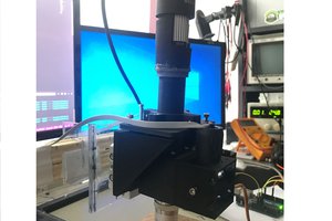
    The optical path was much better, I added a leveling option for the CD optical head and a 45 degre mirror to the top to reflect the image to the CCD of an old phone. I had to remove the optic from the front of the CCD in the phone, surprisingly it worked after all. I also added a Z axis mechanicel movement for better hight adjutment. 

    The resuts was better than before, more details on the images, but I was not happy, because I could not connect the phone to the PC as an USB webcam. The connection is omportant, because if I can not controll the camera from PC, then I am not able to make multiple images and stich them together.

    The result is from the Samsung OLED display:

    The images was cloudy and the CCD had some particle on it sadly.

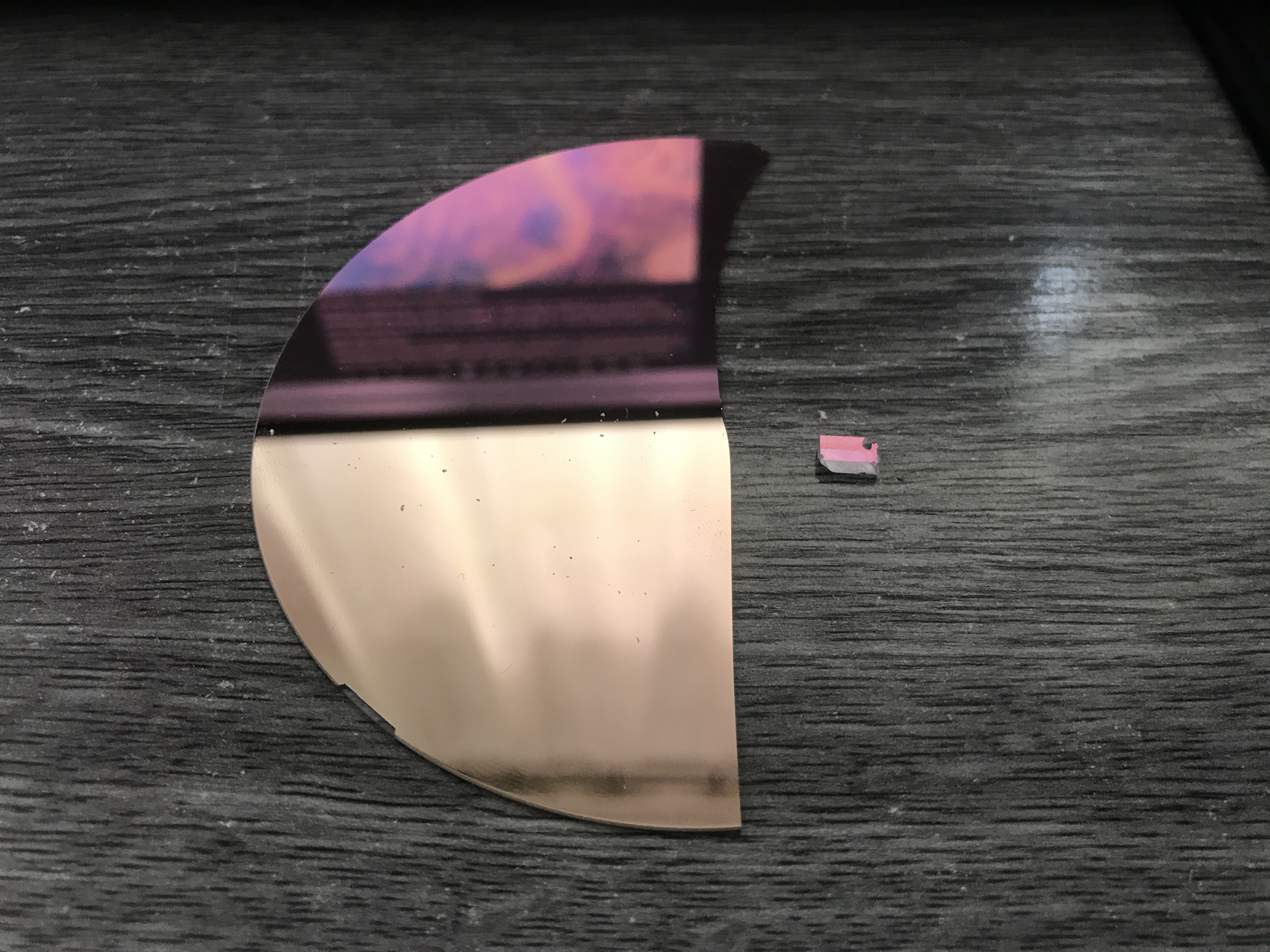
    Because of the connectivity problem, I decided to swich the camera back to the USB microscope camera, with some other changes. I wanted to change the beam splitter because it caused a purple6 violet distortion on the images and I lost a lot of other colors because of that beam splitter. I managed to get a sample, who knows what is the layer on it... But it is actualy much better beam splitter then what I had. It has some orage tone, it reflect the light around 590-600nm. The old beam splitter reflected the light more like above 620nm, so it was not for greate for the low visible light spectra.

    The new splitter material on the left, the old on the right:

    After installing the new beam splitter, I upgraded (downgraded actually) the camera:

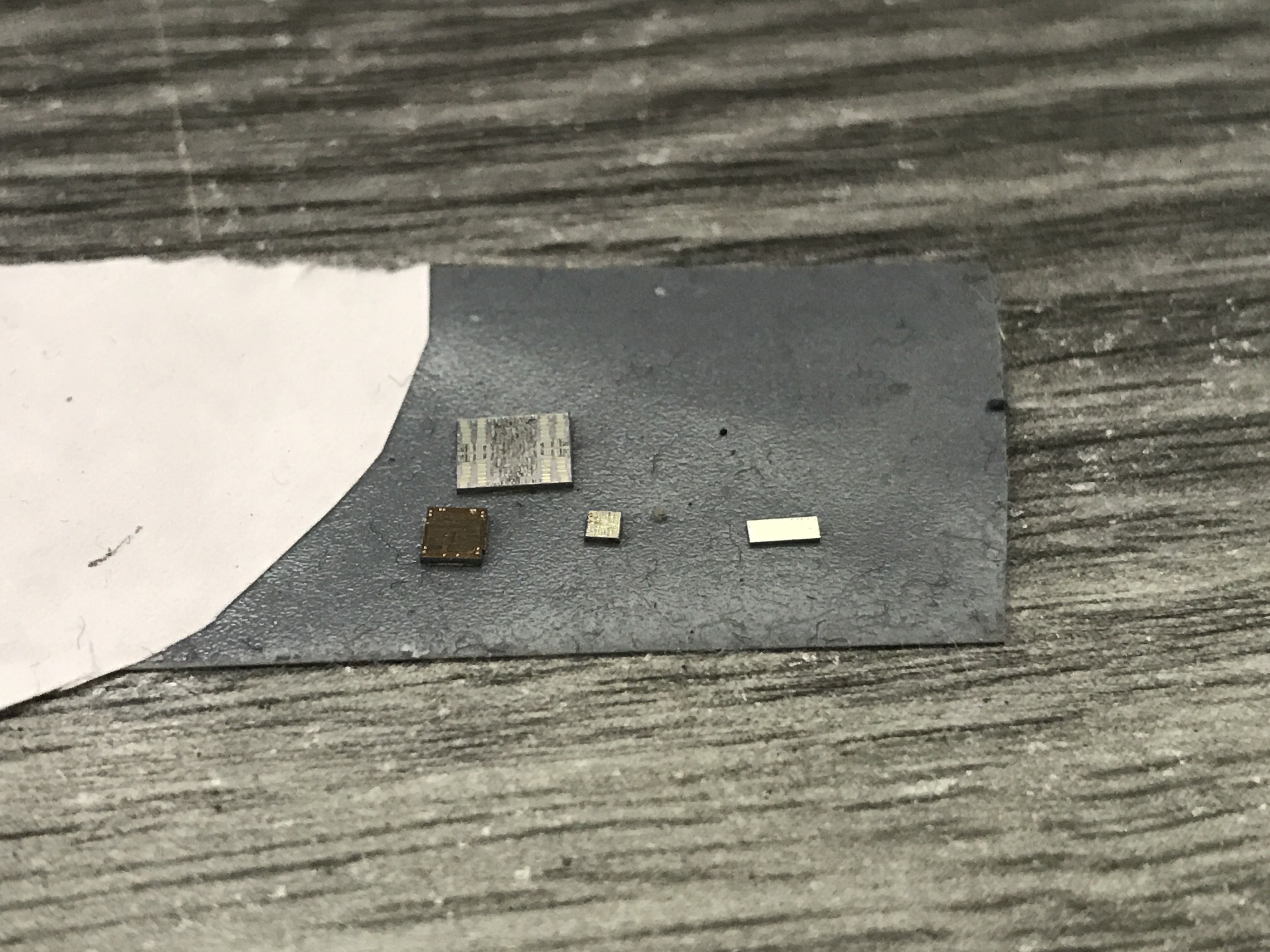
    With the more stable optical setup I decided to try scan an integrated circuit. I managed to harvest some bare integrated circuit component, by heating 500 degrees celsius  IC packs and cracking the open. AN PIC and some analog IC-s:

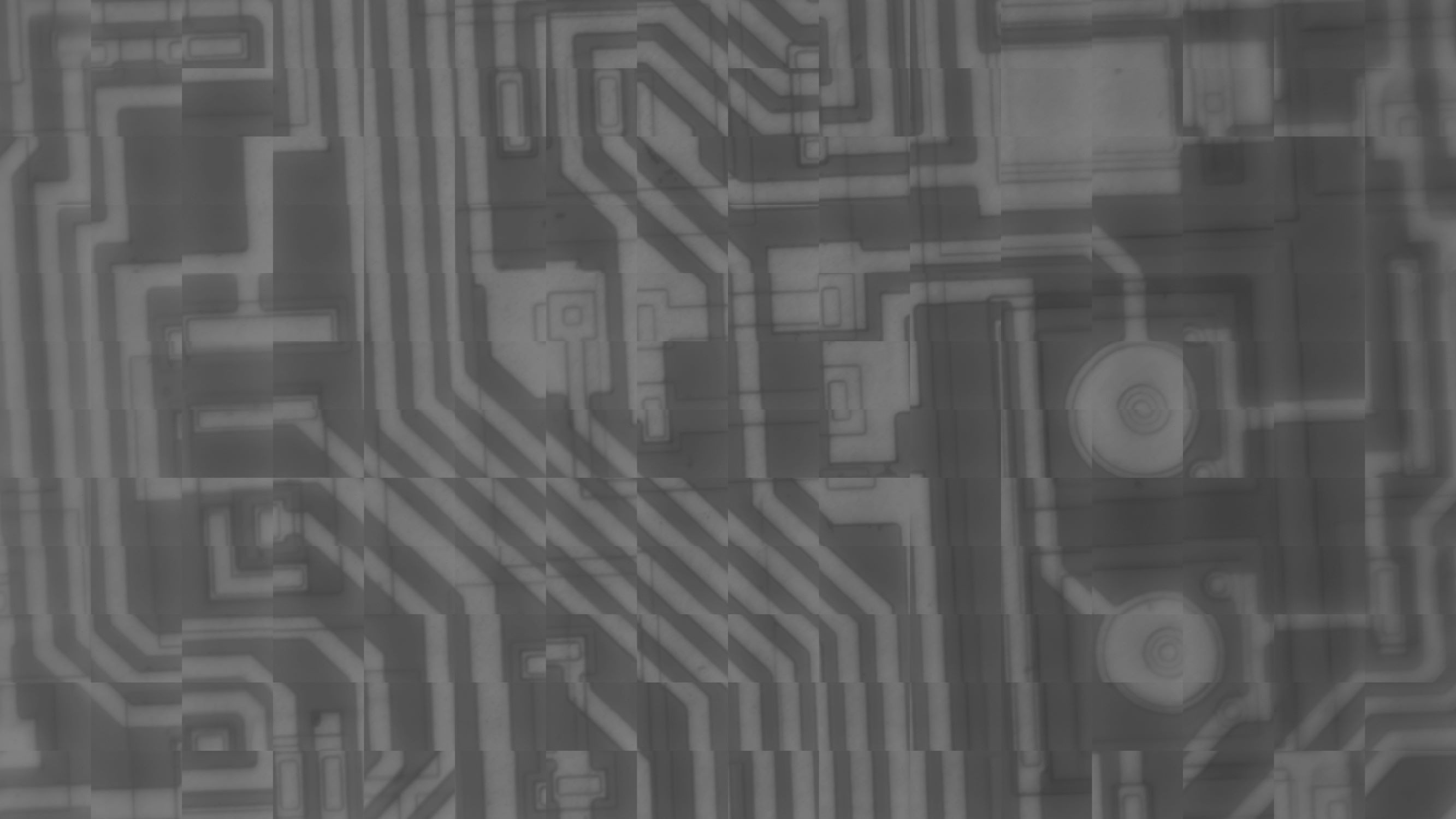
    These much more interresting than screen circuits. The image quality was insane compared to screen circuits. The mechanical movement of the X-Y stage gave me lot of trouble, because it is not precise enough, and wobble a lot. The image stiching is far from perfect I know, but here is the end result of the first scan:

    Originaly it is 56,2MP so it is quite large, I had to convet it to 4MP to upload it here.

    It is a lot to improve...

    My next step is to improve the stiching and get a nice big image, maybe from the full surface area of the IC. 

    In the future I want to try upgrade it to an Imaging  Reflectometer, or make some experience with it at least.

  • Samsung S8+ AMOLED display under the microscope

    Máté Tóth10/22/2019 at 20:13 0 comments

    Microscope picture:

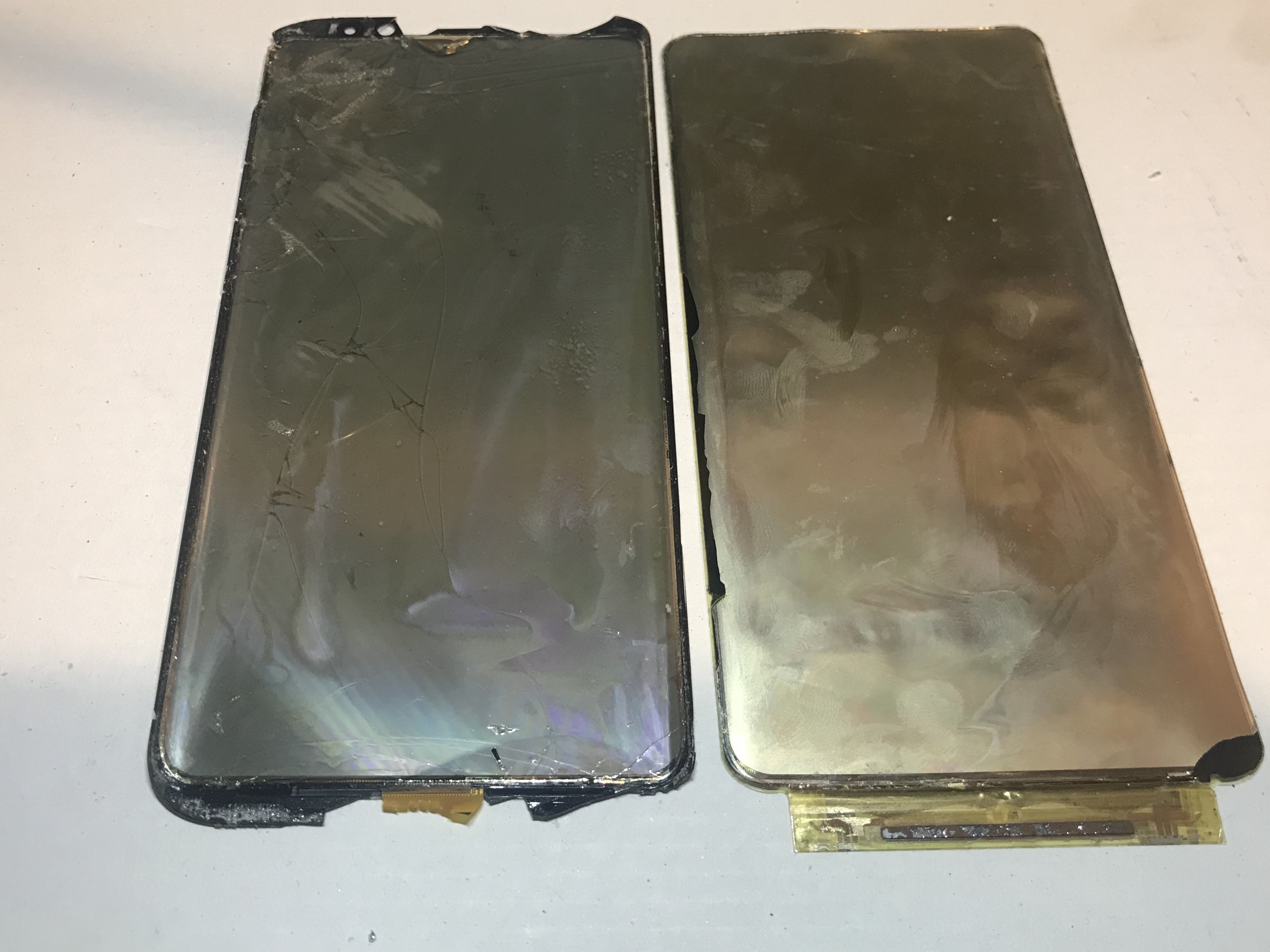
    I asked a local mobile screen repair shop if they may have some damaged LCD or OLED screens for my research, and they said yes and gave me several Samsung S8 and S8+ Amoled screens for free. (Big thanks for the shop manager.)

    As I found out these screens are really good and it looks like Samsung has way more experience over other display manufacturals that is insane. I choose the S8+ display to show, because the regular S8 screen has smaller pixels.

    The S8+ display has the following parameters:

    6.2" Quad HD+ Super AMOLED (2960x1440)
    529 ppi

    It is verry interresting under the microscope, it has a lot of details what I even could not see, because my home made microscope resolution was not good enough.

    So lets see how the pixels looks like when they light up:

    As you see Samsung used  the Diamond pentile matrix. You see some color sub pixels are smaller or bigger. On LCD displays usually every pixel has 3 sub pixel, one RED one GREEN and one BLUE. In this case a full pixel has multiple sub pixels from each color, like one pixel has 4 green sub pixel.

    I am not exactlly sure what is the benefits for this kind matrix, what if I have to guess these AMOLED screens hase much better color accuracy and the pixel will have much homogen light.

    The sepatrated TFT+OLED layer from the front glass+touch layer:

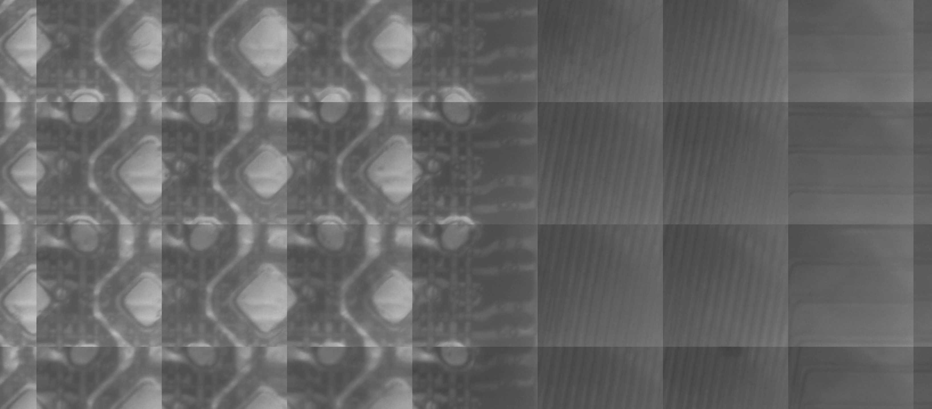
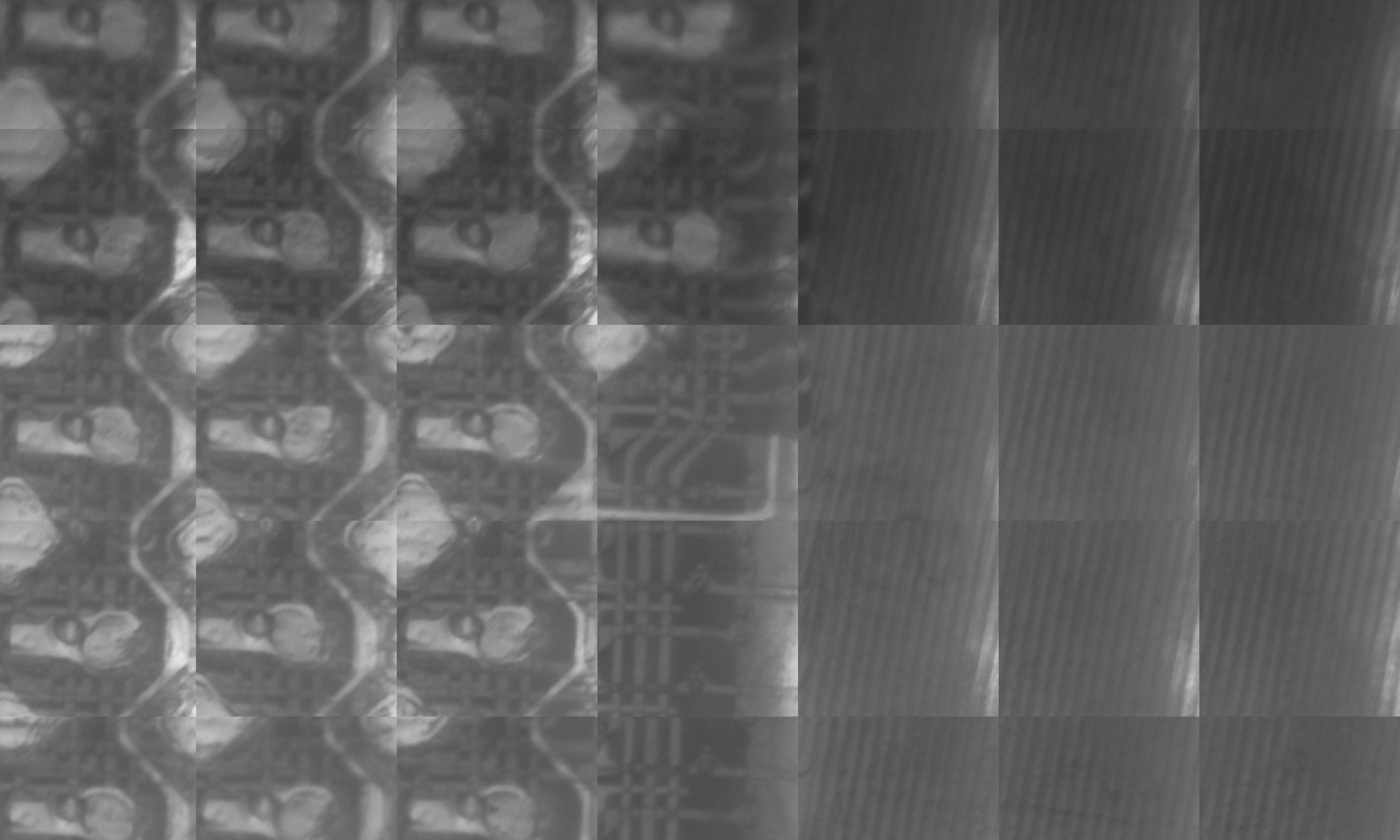
    Now lets see the screen under the microscope:


    This picture was made from several little picture stiched togedher, each picture around 400 x 400 pixel, and the over all picture size is 5720 x 13760 pixel. The over all size is so large I could not upload it to this tread, only just to the download section, so if you are interrested in  the full size pictures, please download them from the download section above.

    Because of touch layer is top of the TFT and OLED layer I had to separate the two layer of the display, so it destroyed it, but it give us the main part what we came for.

    The lines what you are seeing is the electrical trace which are controlling the sub pixels to light. The bigger rectangle is the BLUE sub pixel, the smaller rectangle is the RED subpixel. The GREEN pixel is quite different, it has a round shape. 

    The picture was taken from the bottom of the diplay edge, where the control lines leave the screen on the right.

    The organic layer is sitting top of the TFT layer, so you actually can not see the TFT very clearly. If you are looking closely you will find some little round dots on the lines in the middle those are actually the transistors and active parts.

    The Samsung displays has round edges on the corners, I made a little picture from it, when it is actually starting to "turn" round. You can see on the below picture, it is just missing one horizontal subpixel line from the middle and thats how it starts. 

    I am still working on the improvement of the picture quality, but it is not so easy anymore, because if you just calculate how big those lines on the pictures are, you will find out those are actually not bigger than 10-20um possibly it is closer to 10 microne, so pretty small.

    I hope you find interresting this short article. Please go to the download section for the original size images.

View all 2 project logs

Enjoy this project?

Share

Discussions

Alan Green wrote 08/04/2019 at 23:32 point

This is very cool. Thank you for documenting and sharing.

What are the lighter areas with the rows of 6 darker circles?

  Are you sure? yes | no

Máté Tóth wrote 08/05/2019 at 06:13 point

The lighter area in the midle, is shoud be ground. The circles are inner layer connection.

  Are you sure? yes | no

Similar Projects

Does this project spark your interest?

Become a member to follow this project and never miss any updates