-
Expansion Backplane for SBC v3.2
01/02/2023 at 20:17 • 1 commentHi everyone,
I'd like to share the SBC expansion backplane that I created to pair with the ZTO-80 SBC v3.2.
The design is really simple, and in essence is just a modified version of the Modular Backplane. It's fitted with 5 expansion slots, a power input, a power LED, and a reset switch, just like the traditional backplane. However, it also includes pin headers to connect an external reset switch and power LED, along with the most important distinction, which is a horizontal 40-pin female header, allowing the backplane to connect to a ZTO-80 SBC with a horizontal header. It can also be used standalone as a modular system backplane with no SBC attached.
This board will drastically improve the expandability and flexibility of the SBC, combining the aspects of the SBC and the modular system. Using the backplane, new features can be added to the SBC making it as flexible as the modular system, but the backplane can be disconnected and the two can be used separately, keeping the small size and portability of the SBC.
Here's a review of the PCB layout and features of the SBC Expansion Backplane:
![SBC Modular Backplane v1.0 SBC Modular Backplane v1.0]()
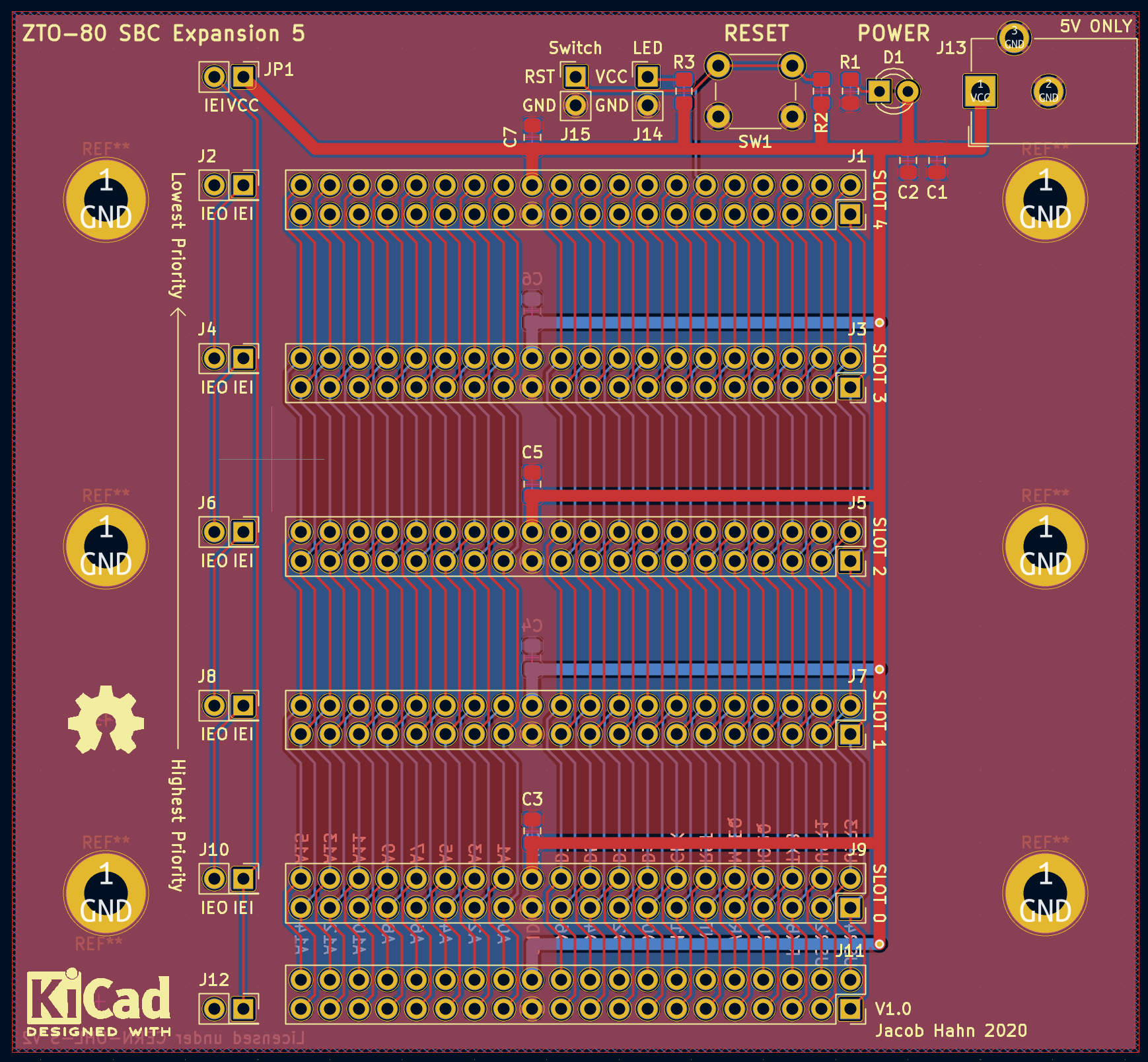
The PCB size is the same as the modular system backplane design, at 3.9 inches long and 3.6 inches wide, with five expansion slots spaced 0.6 inches apart from pin to pin (or roughly 0.4 inches from bottom edge to top edge). Each expansion slot is a standard pin header socket with 20x2 pins and 0.1 inch pitch. Six M3-sized mounting holes provide a way to solidly mount the backplane using standoffs. Compared to the original backplane, the power circuitry has been moved above the expansion slots to make room for the SBC interconnect header.
JP1 is a 2-pin jumper which determines how the Z80 interrupt priority line functions. By default it's open, which leaves the priority line floating so it can be controlled by a connected SBC. However, if closed using a jumper block, JP1 connects the IEI pin of expansion slot 0 to +5V, which allows the expansion board to act as as standalone modular backplane. In short, JP1 should be left open if the backplane is used with an SBC and closed if being used standalone.
Like most of the other ZTO-80 boards, power is 5V only and is not regulated on-board. A 5.5mm barrel jack is provided to power the board while it is being used standalone. If an SBC is connected, only have ONE power source connected at a time, either on the SBC or on the backplane, but never both.
As mentioned previously, the SBC expansion backplane can be used standalone. To do this, simply disconnect the SBC, attach your modular system boards, bridge JP1, and apply 5V power through the barrel jack.
While mostly complete, this board has never been produced and was last updated in 2020. Before publishing it to the GitHub repository, I plan on making a some changes to the board to address some design concerns I noticed. I'm not exactly sure what these changes will be or how major they will be, but I'm going to hold onto the design files until I implement those changes. If you have any suggestions on how I could improve this board, please comment them below!
Right now, my main focus is getting this board and SBC v3.2 fully ready, then I'll move on to updating all of the modular system boards and finally beginning the ZTO-80 CP/M design. Thanks for reading!
-
Back from a long break, plus the state of the project and future plans
12/17/2022 at 20:54 • 0 commentsHi everyone,
It's been about a year since I've even touched the ZTO-80 project, and closer to two since I've made any meaningful updates or changes.
When I started the ZTO-80 project, I was a freshman in high school, and worked alongside my schoolwork to design the computer and document my progress. As I approached junior year, work got more challenging, and I chose to focus my efforts on school, the robotics team I was part of, and film photography, a new hobby I had just picked up.
Fast forward to now and I'm about to go into my second semester in college, where I'm studying electrical and computer engineering. I heavily referenced my work on the ZTO-80 project in my college applications, and it was a big reason I was accepted to the college I'm in now.
College has reignited my interest in engineering, and for a while I've been trying to find an excuse to continue working on the ZTO-80. I left it while I still had tons of ideas for future designs and features, but I just haven't had the time or motivation to sit down and do the work required to implement them. But now that I'm on winter break and have a few weeks of free time to get things in order, I've decided to pick the project up again.
Obviously, picking up a project after two years of neglect isn't easy, but all of the documentation I've kept should make it a lot easier for me. Once I get up to speed again, I have a bunch of ideas I can work with. Here's a non-exhaustive list:
- SBC Modular Backplane. In my last project log, I mentioned that I was creating a modular backplane to connect to the SBC. This board has been designed and I plan to continue with that idea. Keep an eye out for a future project log dedicated to that.
- ZTO-80 CP/M. I'm reaching the limits of a computer with no operating system, and can only run code in either BASIC or Assembly. I have plans to design a ZTO-80 SBC (and potentially a modular system as well) which is capable of running CP/M, a common operating system in the 1970's and early 80's which could run on the Z80. This will require significant hardware changes and would be a big project, so expect a delay before updates. I will still support and update the BASIC ZTO-80 while I work on the CP/M version.
- KiCad migration. When I first started this project, I was using EasyEDA to design my boards, but I quickly moved over to KiCad and have since been using that. However, most of my modular system boards are still in EasyEDA. Because some of these modules need improvements anyways, I will be redesigning each module in KiCad.
- Organization changes. I plan to make changes to how the GitHub repository is organized in order to provide more files and make them easier to access. This will also help me stay organized as I work on the project.
- Updating documentation. As well as better organization, I plan to update the ZTO-80 project pages and documentation (here and on GitHub) to better describe the goals, capabilities, and future improvements to the project
- And more!
I'll be working on all of these ideas and posting project logs and updates as I do, so stay tuned for that.
Obviously, college isn't easy, and I may not be able to work on the project consistently, but I'll definitely be working while I can and update as often as possible!
-Jacob
-
The ZTO-80 SBC is for Sale
10/01/2020 at 16:45 • 0 commentsOver the past couple of weeks, I've been getting everything ready for the v3.1 boards to be sold online.
After receiving the new boards, plus parts to make one board, I soldered one and tested all of the features using the same methods I used to test v3.0. All of the issues that I had identified were successfully fixed in this revision.
I also rearranged the headers to be mostly concentrated on one side of the board. This improved the usability of the board's features slightly, as a breadboard can be placed on one side of the board and easy access most signals.
Now that the boards were designed and tested, I decided to work on selling them on Tindie. This required a few steps: setting up the Tindie shop, taking photos, and preparing shipping. The most time consuming of these steps was shipping. I had to figure out a good base rate to charge for anywhere in the US, and also one for certain international destinations (which is harder, as different countries cost different amounts to ship to). I also had to choose what packaging I would use to ship the board. To do all this, I took a few trips to the post office and sorted everything out. I'm now confident that I'm giving the best deal I can on shipping to anywhere in the US and some international destinations.
At the time of writing, I have 7 boards in stock. I'm not expecting to sell many at all, so I believe that will be more than enough for now!
You can find the Tindie listing to buy the boards here. I appreciate every sale I get and each one motivates me to continue to work on the project.
Next up on the project agenda is to complete the modular system. This includes a backplane that can attach to the ZTO-80 SBC using the expansion header and horizontal headers. When I get to a good spot, I'll post an update.
-
Testing v3.0
08/30/2020 at 03:57 • 0 commentsHi everyone,
Over the past couple of weeks, I've been working hard to test all of the features of the SBC v3.0.
When I first plugged in the board to test it after soldering, I was sad to find that it did not work immediately, which I had hoped it would. This was because of two issues. First, I hadn't updated the software to support the new SIO addresses, which were changed since v2.0 to be more standard. That was an easy problem to fix. The second reason was due to an issue with my schematic. I had incorrectly wired the I/O decoding circuitry enable pins, so it was never activating the SIO. I fixed this by cutting some traces and adding jumper wires.
After that, the board booted, so I could test the rest of the features. The first obvious feature issue was that the footprint for the DB9 serial port was incorrect. Apparently, KiCad's library was using a footprint that was outdated and not used in any existing DB9 connectors. Up to that point I was using the TTL serial port to control the board and hadn't inserted the MAX202 chip. However, when I did, the TTL serial port stopped working. This was because of an internal pulldown resistor in the MAX202, and it was impossible to bypass. Due to all the issues plaguing the full serial port, and due to the fact that removing it would take a chip and 5 capacitors with it, I decided to remove it from the design.
The next issue was the PIO. This was only a minor issue and didn't truly affect the design. I had forgotten that the ULN2803A was inverting, and so it would make more sense to break out VCC on the Channel B header than it would to break out GND. I changed this on the schematic, but on the setup I have I used the VCC pin on the expansion header to provide power to my LEDs I used to test.
Finally, I tested the CTC. To do this, I wrote a little piece of code that would print "TIMER DONE" whenever the timer finished. I chained two CTC units to get an output about every second. This code worked flawlessly, and so I know the CTC works fine.
Now, I'm all set to get an order of the final v3.1 prototypes. If all goes well, I will then be able to order the final production batch and begin to sell them. I'll update you then.
-
Behind the Scenes Work
08/18/2020 at 03:59 • 0 commentsRecently, I took a break from working on this project to keep up with school and work on a few other more pressing things. However, when summer came along, I decided to continue to work on the ZTO-80.
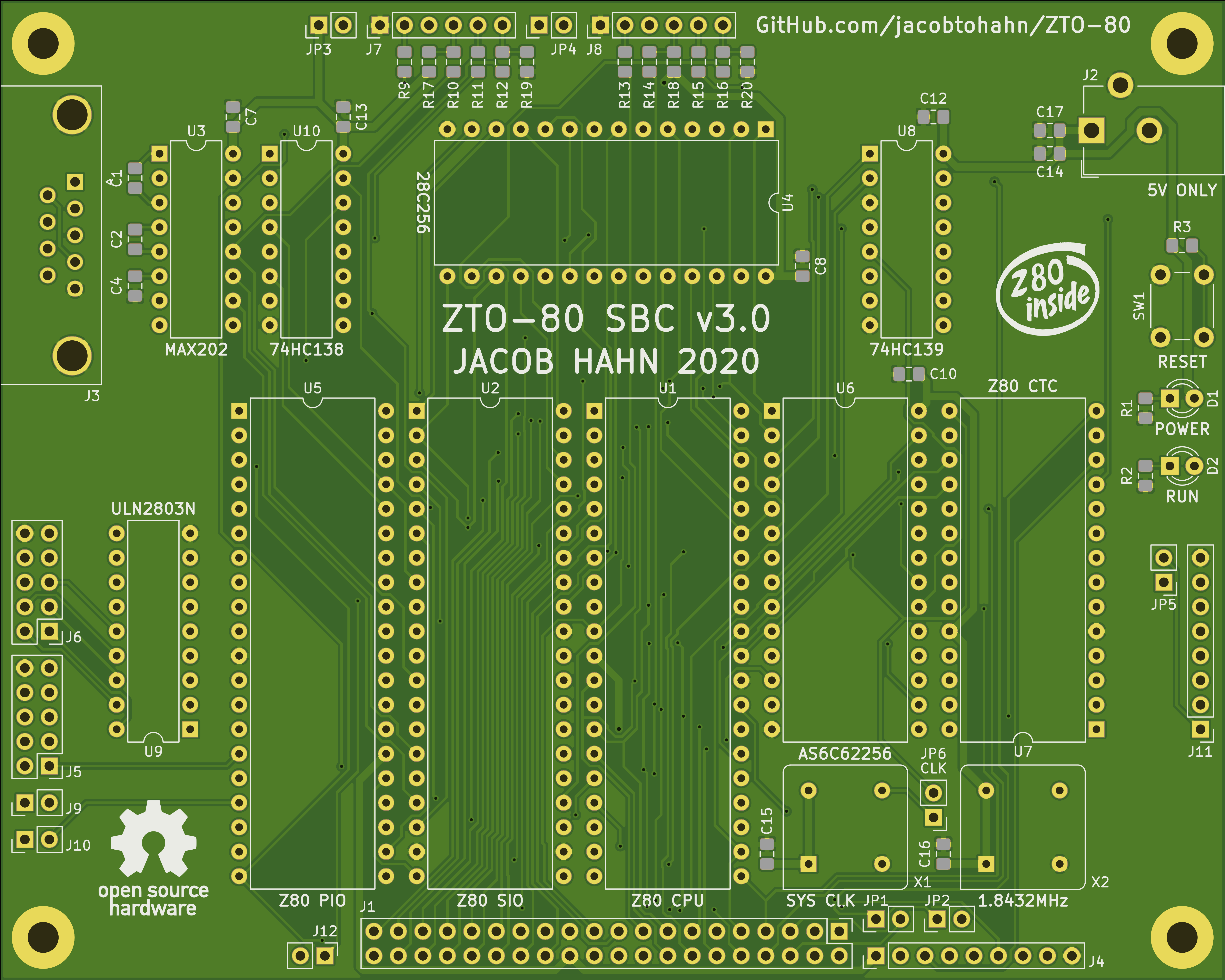
So far, I've done tons of behind the scenes work to improve the project. I've ported nearly every board to KiCad, and redesigned the SBC into version 3.0, which adds more functionality and customization than the last boards in the series. I'm beginning to think that this is the most I can fit on an SBC (look at all the traces!), and so I'm planning on making a modified version of the backplane that can attach to the SBC.
![]()
One of the biggest changes I've made is creating a GitHub repository for the project, where I'm now hosting the latest versions of all ZTO-80 PCBs, along with the latest port of BASIC. You can find everything you need to make the project there. Whenever I make changes, I upload them straight there, so you always get the latest revision. Currently, I'm still modifying and finalizing the designs, so I would hold off until I test the designs before you order your own PCBs. You can find a link to the repository in the links section of this project.
Another thing that I've made is a full user's guide to the SBC. It includes everything needed to get started with the SBC, including a BOM, assembly instructions, and software installation instructions. You can find it in the GitHub repository under PCB/SBC/.
Also, I'm creating a Tindie store to sell the SBC and modules for those who don't want to deal with having them fabricated themselves. The first product, hopefully coming in just a couple of weeks, will be the SBC. I plan to sell both the bare boards and also kits with all the parts included.
I have prototype boards for the SBC v3.0 on the way from JLCPCB right now, with an estimated delivery of Friday, so you can expect an update then.
In the near future, I plan to give this project page a much-needed overhaul. Stay tuned for that.
-
Testing out KiCad and my Issues with EasyEDA
01/22/2020 at 14:25 • 0 commentsUp until this point in the ZTO-80's development, I have been using EasyEDA as my main EDA program for making schematics and laying out PCBs. It works well and has all of the features I need while still being very easy to use. It also has simple integration with JLCPCB, which is where I order my boards. It does, however, have its drawbacks. Being an online service, you can't use it without an internet connection. Furthermore, although it has an extensive library of user-created symbols and footprints available, the included symbols are unorganized, not always well made (unless they are linked to LCSC), and somewhat difficult to modify. This isn't helped by a poor interface to choose parts and lacking library management. While the integration with LCSC is helpful and provides good symbols, the service doesn't have most of the parts that I need and I prefer DigiKey. It also isn't widely compatible with other programs (such as KiCad).
Due to these reasons, and also because of the potential volatility of EasyEDA's free plan in the future, I have chosen to migrate to a new EDA software. I originally thought that I would move to Eagle, as it is well known in the industry and has much documentation. However, I didn't like the limitations of the free version, so I looked elsewhere, settling on KiCad. It's open-source, completely free, capable, and supported by organizations such as CERN.
I followed the very helpful Getting Started guide on KiCad's website, and quickly learned my way around the software and designed a test board. I'm still getting used to the new workflow, but I can already tell that it will be much easier to manage than EasyEDA.
One issue with migrating to KiCad is that EasyEDA doesn't have a feature to directly export to KiCad. After looking around, I discovered this script, which is supposed to allow export to Kicad from EasyEDA. Text doesn't come out very well, but the rest seems fine. Even with this script, though, I probably will just end up using the dimensions of my boards to port them by hand.
I still plan to use EasyEDA for smaller projects and all my current designs will still be hosted there, but expect me to upload KiCad files to this project in the near future!
-
First Working Modular Prototype!
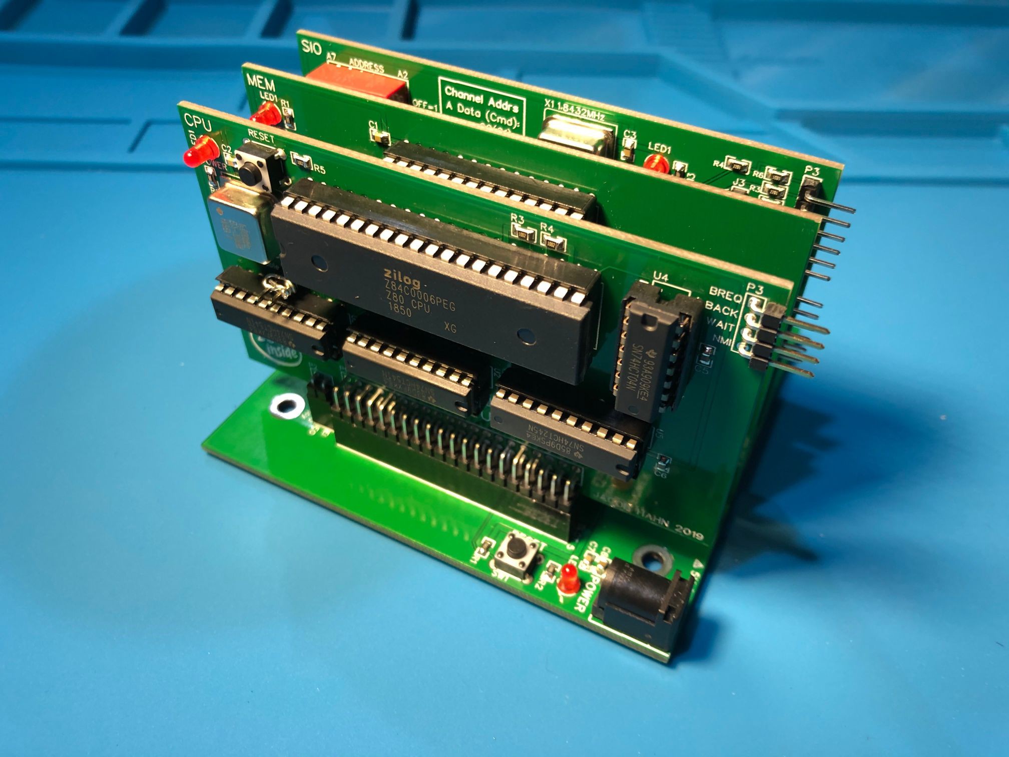
01/04/2020 at 06:36 • 0 commentsIt's been quite a while since I've last posted, so I thought I'd update on what's been happening in the meantime. I've been working hard on the modular ZTO-80 design, and finally ordered the boards. I changed the pinout of the bus multiple times, finally landing on a version that keeps efficient trace routing for both the Z80 CPU and other peripherals. To keep things as simple and expandable as possible, I split the CPU and memory into their own modules. Currently, then, I have created a backplane, CPU card, 64K memory card, SIO card, PIO card, and a front panel board. The CTC card has not been designed yet.
![]()
![]() ---------- more ----------
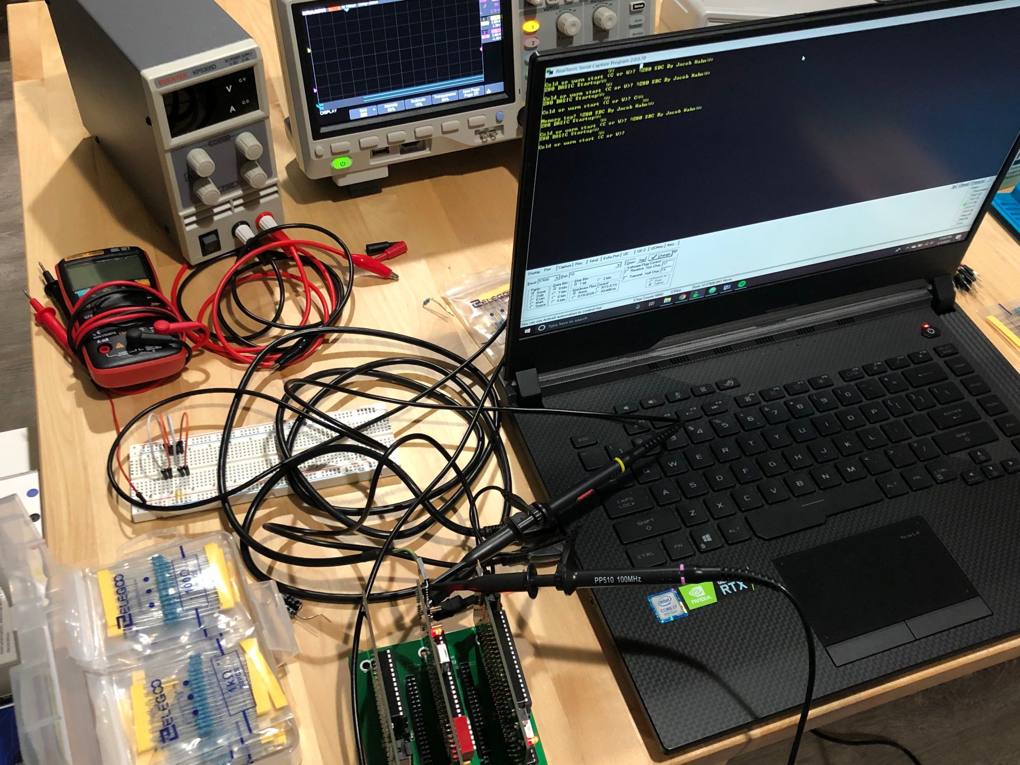
---------- more ----------So far, I have soldered and tested a minimal system, using the CPU, memory, and SIO. After changing the address of my SIO in code, I booted basic to find that it worked. However, the computer refuses to respond to input after a single character has been sent until it is reset. I verified this issue using an oscilloscope on the SIO's port A RX and TX lines. Port A was connected to my computer. Using the decode function of my scope, I found that the data was being sent and received intact. This whole issue is confusing, as the code is exactly the same as what has worked on the SBC, with only an address changed. I'll have to keep looking around the system for problems and to check if it's software or hardware. Does anyone have any idea what could be causing this? I'm sure the front panel will be super useful as a troubleshooting device!
Here are detailed descriptions of each module of the ZTO-80 Bus System:
Backplane: The most important part of the system. The backplane I have designed contains 5 ZTO-80 Bus slots spaced .4" apart. Besides the slots, it has a standard jack for 5V power, smoothing capacitors, a power LED, a reset switch, and the slot pinout on the back. You could design your own backplane with more slots (if you keep the same board height of 3.9"), but 5 was the most I could fit without the width exceeding 100mm, which would raise the price.
CPU: The heart of the system. The bus was designed around the Z80, so that's what I'm using. The other major features are 74HCT buffered address and data lines to accomodate a TTL or CMOS Z80 and lots of modules, a breakout pin header for useful lines not included in the bus (I may add HLT to this in the future - I overlooked it!), and a slot for a system clock for whichever speed CPU you choose with a clock enable header.
Memory: The most basic card. It contains 3 ICs, specifically the RAM, ROM and an address decoder. The max memory supported is 64K, but a card with bank switching could add more.
SIO: This serial I/O card is used to communicate with a serial terminal, PC, or other serial device by means of a Z80 SIO/0 or DART (careful with the DART - it's a TTL chip in a CMOS system). There are two serial ports, with port B optionally connected to the TX/RX pins of the bus. The baud clock is included on the board. There is also a new address decoding system, utilizing an 8-bit magnitude comparator to allow for a total of 64 unique, tightly-decoded I/O addresses, programmable by a DIP switch.
PIO: A simple card based on the Z80 PIO. The design is exactly the same as the SBC, with two 10-pin headers for the channel outputs. Channel B includes a darlington transistor array for a max current of 500mA per pin. The module uses the same address decoding system as the SIO.
Front Panel: The earliest "personal computers", which used a 100-pin bus called S-100, had control panels on them to both monitor and manipulate the address bus, data bus, and control signals. I have designed a similar board for my bus which shows the address and data buses and some control signals using LEDs. At 6 MHz, the board is essentially useless, so I also implemented an instruction single step circuit that makes use of the WAIT control line to allow instructions to be run one at a time using a pushbutton, all without stopping the system clock. This feature can be enabled or disabled using a slide switch.
-
A Change of Plans and a New Design
10/30/2019 at 04:26 • 0 commentsIn the last log I posted, I had said that I would be ordering PCBs for my new SBC V2.1 design. However, after refining the schematic and PCB as much as possible, I decided that along with the SBC, I would build a modular, backplane-based design to allow for much more versatility, easy prototyping, and lower costs. Along with this, I decided I should finally give my project an official name. Z80 SBC is far too generic and could refer to any SBC design. Thus, the ZTO-80 was born.
The name ZTO-80 is the name of the general design of my Z80 system. It can be used to refer to either the SBC or the newly-made 40-pin bus I have designed for the system. The name itself comes from a combination of Z80, as this is the processor the system is built around, and my middle initials, T and O (yes, I have two middle names).
While the design of the ZTO-80 SBC has remained about the same since the last update, I decided that instead of having to order a completely new SBC everytime I made a change, I could break the main functions of the SBC into modules and order the new individual module when I changed something. As of now, there are 5 main parts of the ZTO-80 modular system: the backplane, CPU/Memory, Serial I/O, Parallel I/O, and CTC. Except for the backplane, all of the modules are on cards. Because the modules are seperate, unneeded features can be left out, reducing the cost of the system and adding space for custom modules.
The bus has been created to keep the most important signals from the Z80, such as the address and data bus, I/O and memory control lines, the clock, and interrupts, while leaving out non-essential signals, such as DRAM refresh and BUSREQ/BUSACK. This creates a bus that uses only 34 of the 40 available pin. Two of the remaining pins are used for TX/RX (only one module can use these signals at a time, modules should have jumpers instead of connecting directly to these lines) and the last 4 pins are left open for the user.
I will still be updating the SBC, and with this new design created I may also redesign the SBC to have much more efficient routing.
On my EasyEDA page, I have created a project that outlines the template for the design of a ZTO-80 module. It should be a very useful resource for creating cards of your own.
P.S. Grant Searle's page for his 7-chip Z80 computer was closed for some reason or another, and I couldn't find a new version, so I just replaced the link on the project page with an archived copy.
-
V2.1 is on the horizon!
09/29/2019 at 04:27 • 0 commentsRecently, I have been putting my full focus of the project on designing and refining the SBC V2.1. I have some great new features on it while keeping the PCB just about the same size. The largest of the additions is likely the new expansion bus, which has been designed to be very similar to RC2014 (albeit with some slight variations to make the design easier to manage) and allows for nearly endless amounts of freedom to expand the board. It has been implemented with a 40-pin header just like on V2.0. Next is the addition of a TTL serial port that is connected to channel B of the Z80 DART. The port is using an FTDI cable pinout, so cables are easy to find. With a little work, the port could be made to communicate with a device such as an Arduino or Raspberry Pi to add something like a USB keyboard.
Along with these major changes, I have added some small fixes and edits. One of these changes is leaving no inputs floating, so the board should be reliable for CMOS chips. I've always used a CMOS Z80 and peripherals without problems, but now it's guaranteed to work. I've also added two pins to the PIO headers. One pin (pin 10) is a ground pin so that it's easier to ground your connections, and the other (pin 9, only on port B) is a common cathode pin for the flyback diodes on the ULN2803A. No more fried transistors from your motors! Pin 9 is left unconnected on port A as it doesn't have a transistor array.
While working on this design, I had the idea to make a smaller version of the board that has the PIO, CTC, SIO + serial ports, and power jack removed, allowing it to be very compact and easily usable in a backplane-based environment. It would also be cost effective, as it would be under 100x100mm. Of course, the downside to this design is that it would have to be used along with a backplane and at least a serial board. Do you think I should create it? My current board is too large to be reliably used on a backplane, so I'll probably use a ribbon cable to connect it temporarily.
I should be placing an order for the new boards within the next few weeks.
-
Progress Update: CTC Tests and PCB Revisions
09/23/2019 at 03:26 • 0 commentsFor the past few days, I've been working on developing a simple test program for my CTC. The goal of the software is to print "Timer start", wait 1 second, and print "Timer done". The timer runs off of the system clock (6MHz) so that it can be divided into exactly 6Hz. This is done by setting up a timer with a 16x prescaler and 250 time constant, the zero output of which is fed into a counter which counts down 250 events. Each time the counter hits 0, it throws an interrupt, which the CPU then handles using an interrupt routine. Each time the interrupt routine is called, the CPU adds 1 to a memory cell. If the cell is equal to 6, the timer is finished and "timer done" is printed, ending the program. The math ends up looking like this:
(((6000000/16)/250)/250)/6 = 1Hz
Therefore, the timer lasts for exactly 1 second. Of course, you can change the duration of the timer by editing the value in the RAM cell that the program checks for. You can find the code here.
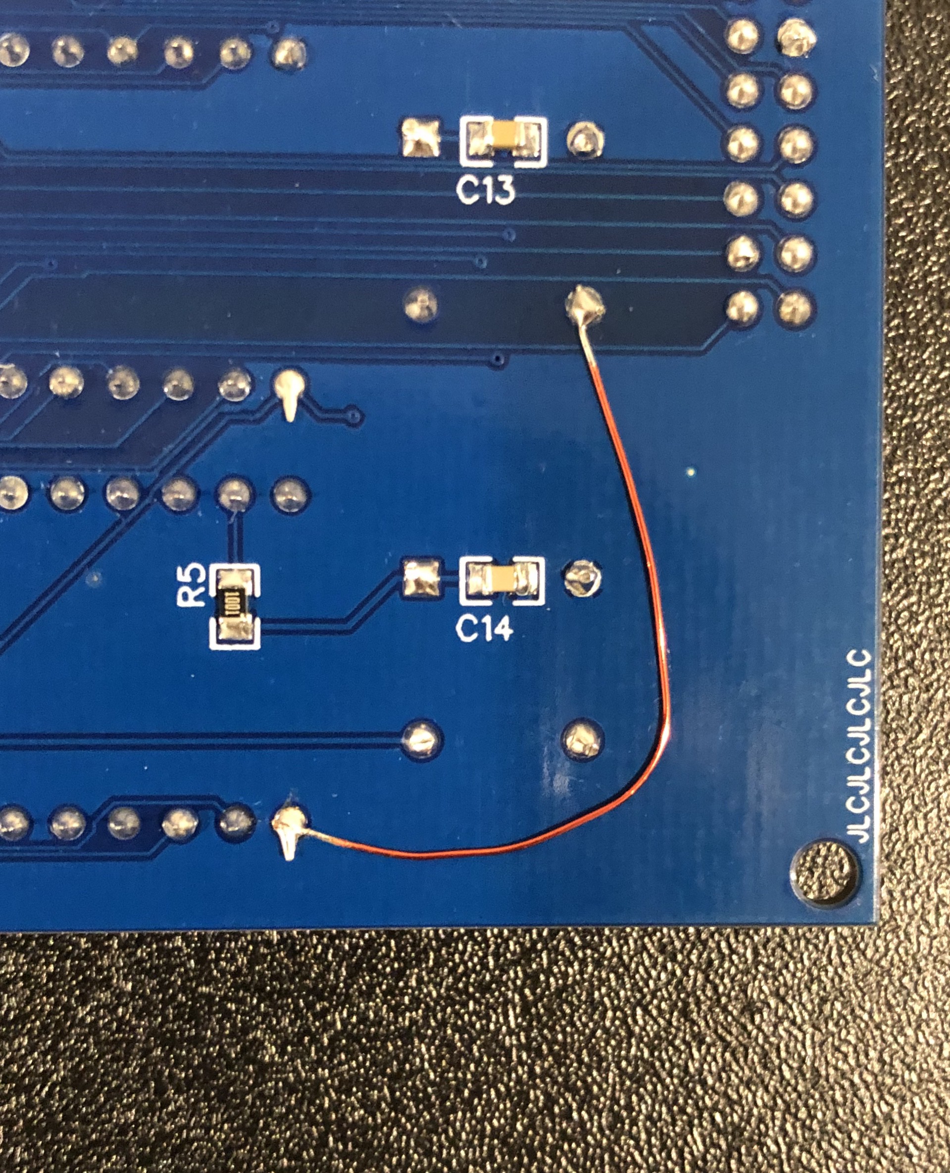
As usual, there were some hiccups along the way. As I was testing the program, I realized that the CPU was never running its interrupt routine, which meant that either the routine was programmed incorrectly or that the CPU was never receiving a pulse on its INT pin. The problem happened to be the latter of the two, and so I looked over my CTC programming to see if I had made any kind of mistake, which I hadn't. With software out of the way, I began to debug hardware. After analyzing my PCB schematic, I noticed that I had hooked the baud clock signal up to the CLK pin of the CTC. I had done this on purpose, as the baud clock could be easily divided into exactly 1Hz using only one timer. What I failed to realize is that this caused the CTC to be out of sync with the CPU (duh) so they couldn't communicate. Oops! With an X-Acto knife and a bit of enameled copper wire, I was able to hook the main clock signal up to the CTC and disconnect the baud clock.
This wiring issue, along with a few other issues, have been fixed in version 2.1 of my PCB. The most important of these fixes include better CMOS support (no inputs left floating), moving the ROM socket for easier access, adding a TTL serial header on the SIO channel B, GND pins on the PIO headers along with a common cathode pin for the flyback diodes on channel B, and some general layout changes.
I should have some new PCBs within a few weeks and I'll update on any changes before then, as well as updating the project details section.
ZTO-80 Computer System
A powerful Z80 computer built around a highly expandable central bus design
 Jacob Hahn