-
1Tools and Materials
![]()
The following tools and materials were used in this tutorial:
- 10W laser engraver (link / link / link). It was used for printing the circuit drawing on a blank copper PCB board.
- Copper PCB (link / link / link). Homemade circuit boards are usually printed on copper coated phenolic plates. The whole surface of the board is coated (on one side or both). Copper is a conductive material, while the phenolic substrate can't conduct electricity. By removing parts of the copper layer, one can create tracks between the components, creating the circuit board.
- Latex PVA water based ink. As you will see later on this tutorial, I used water based ink to create a mask on the surface of a copper PCB. This mask prevents parts of the copper layer from being removed by the ferric chloride solution.
- Paint brush. A thick layer of paint will have to be applied on the circuit board, and a paint brush will be usefull here.
- Ferric chloride. This comes as a salt and should be dissolved in water before it's used. This solution is able to corrode copper, removing it from it's phenolic substrate. Apply a mask and only the parts of the copper plate exposed to the solution will be dissolved.
- Sandpaper. In the end, you'll have to remove the remaining mask from the board. This can be done easily using a sandpaper.
-
2Homemade PCB Manufacturing Process
The manufacturing process of homemade PCB usually consists of the following steps:
1. PCB design
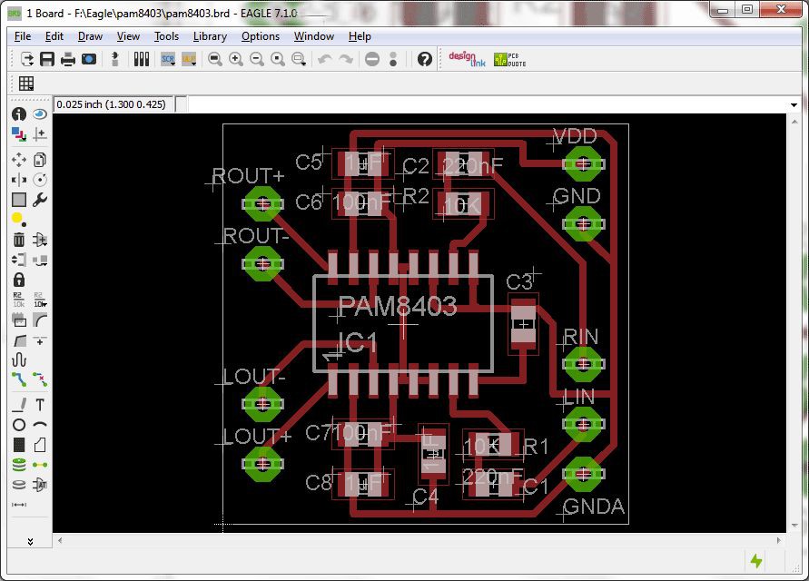
In this step the drawing of the board to be produced is made. It is possible to both design a new board and make copies of opensource projects. Different CAD software can be used (Fritzing, KiCAD, Proteus, Eagle, etc.).
2. Apply a mask on the PCB
Once the printed circuit board is designed, it must be transferred to the circuit board. There are several ways to do this: using the thermal method (by transferring toner from a sheet of paper to the plate, by applying heat), manually (by drawing the circuitry with a suitable pen) and even using a 3D printer. In this project, I used a laser engraver to transfer the design to the plate.
3. Chemical etching the PCB
Once the mask is transferred to the plate, corrosion of parts of the plate is performed to remove parts of the copper. At the end of the process, the board should only be with the tracks that make up the circuit.
4. Cleaning and finishing
Once the corrosion is complete, the plate will be ready to be cleaned, drilled and the components welded. After that, just check everything, power it up and be happy!
-
3PCB Design and Creating the Mask
Once you have a PCB design (designed using any CAD software of your choice) you can export it in SVG format for reading in other graphic editing software. Several layers can be exported in this process: top view, bottom view, mask, silk, etc. All layers are available in normal or mirrored format. The fabrication process described in this tutorial requires that a mask be applied to the PCB. The part of the cover plate that is covered by the mask will not be corroded and will therefore be retained on the end plate. Parts that are not covered with the mask will be exposed to the iron chloride, being corroded and removed from the printed circuit board.
![]()
In this process it is necessary to coat the entire plate with a layer of paint, and remove only a few sections using the laser engraver.
In this way, the mask generated by most software should have its colors inverted (invert the black pixels to white and vice versa). To perform the mask inversion, two softwares were used:
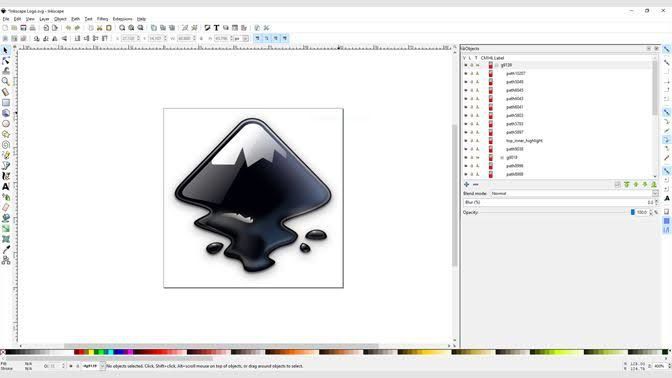
- Inkscape: used to convert SVG files into image format (PNG). Also used to transform the drawing into a black and white image (if the CAD export in color format);
![]()
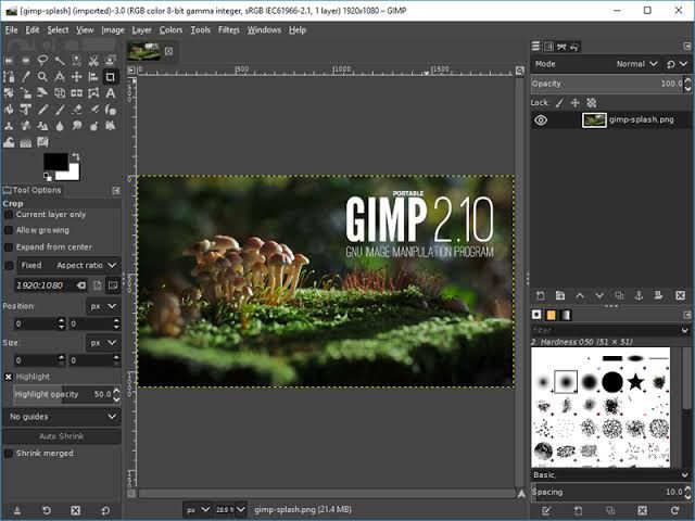
- Gimp: used to invert the mask color (white pixels in black pixels).
![]()
The resulting image is then loaded into the laser engraver software for printing to the surface of the plate.
Pay attention to the dimensions of the image: check that the output dimensions of the laser engraver software are the desired ones for the actual prototype.
![]()
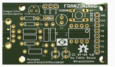
In the case of this tutorial, the design of a specific board was not done. Instead, I tried to replicate an opensource board, developed by Fábio Souza: Franzininho. This incredible board can be easily assembled and programmed by users of all levels, it is compatible with the Arduino IDE and entirely designed in Brazil!
More information about the board in the Github project: https://github.com/Franzininho/franzininho-diy-board
![]()
-
4PCB Preparation
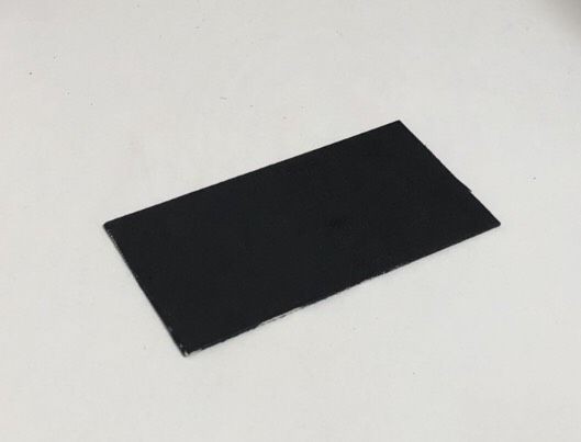
Once the mask is designed, it is possible to start the PCB production. The first step is to apply a more or less uniform layer of paint onto the plate. In my case, a water based black PVA latex paint was used. It is important that the paint is as dark as possible so it can be burned by the laser. A white paint can reflect the laser, reducing its effectiveness.
It is also important that the paint be water based to facilitate its removal from the plate after etching the copper board.
A single uniform layer of paint was applied onto the plate, leaving the surface fully coated. It is important that there are no holes or imperfections, as they can create unwanted points of corrosion, damaging tracks or creating unwanted points of contact.
It is necessary to wait for the paint to dry completely before moving on to the next step.
![]()
![]()
-
5Laser Engraving
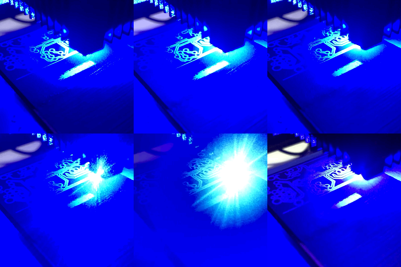
Once the paint is dry, you can use the laser engraver to remove unwanted parts from the mask.
A 10W laser engraver was used as shown at the beginning of this tutorial.
For the production of the board, the following parameters were used:
- Laser intensity: 100%
- Speed: Maximum
- Burning time: 20 ms
- Shortest path
If a different equipment is used, a combination of these parameters must be tested to obtain a better result.
![]()
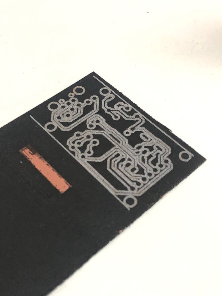
The laser doesn't have sufficient energy to puncture the copper plate, but is able to remove the paint, exposing the copper layer under it.
It is important that at the end of this step the circuit is clearly printed on the board (remembering that the dark parts will not be removed after the corrosion, and that only the part of the exposed copper will be corroded).
The process may be slow (depending on the dimensions of the board and the amount of material to be removed). Therefore, it is important to limit the area to be burned to the maximum possible, using the
![]()
copper-filled tool available in most CAD software (Fritzing, for example). Otherwise, considerable time will be spent in removing the ink from sections of the board that do not interfere with the functioning of the final circuit. In addition, limiting the amount of copper to be removed from the plate through corrosion also helps to increase the life of the iron chloride solution, since the oxidation reaction will be less. Thus, more prototypes can be produced before the need to exchange the corrosive solution.
Beware of printing time (limited by manufacturer's recommendation). It may be necessary to take breaks periodically (every 10 minutes, according to the recommendation of the model used in my case).
The printing of the approximately 50mm x 25mm board tested in this project took about 30 minutes. Well more than I expected at first, but still an acceptable time for a prototype.
![]()
![]()
-
6Chemical Etching
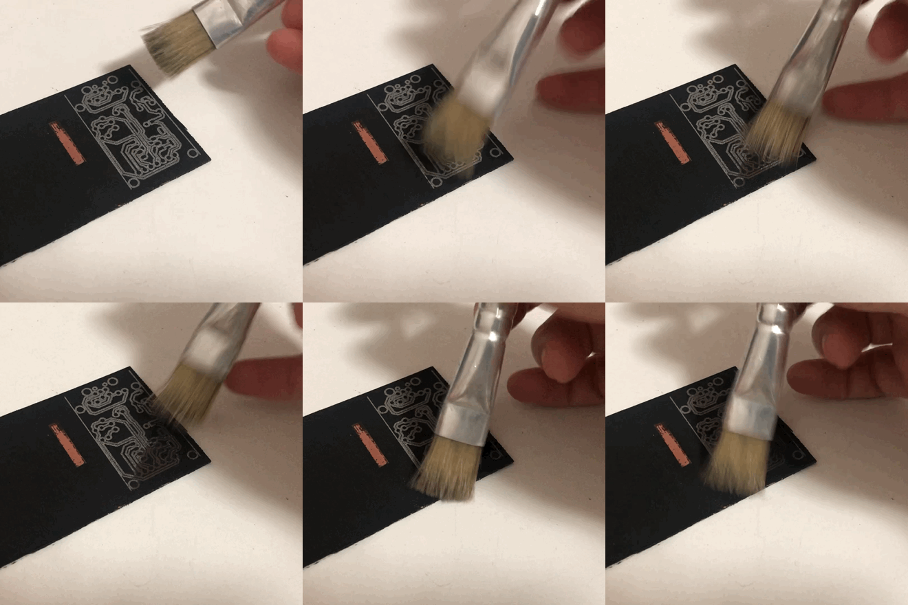
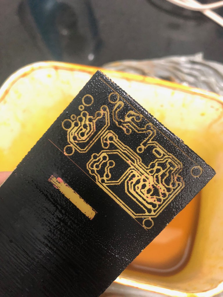
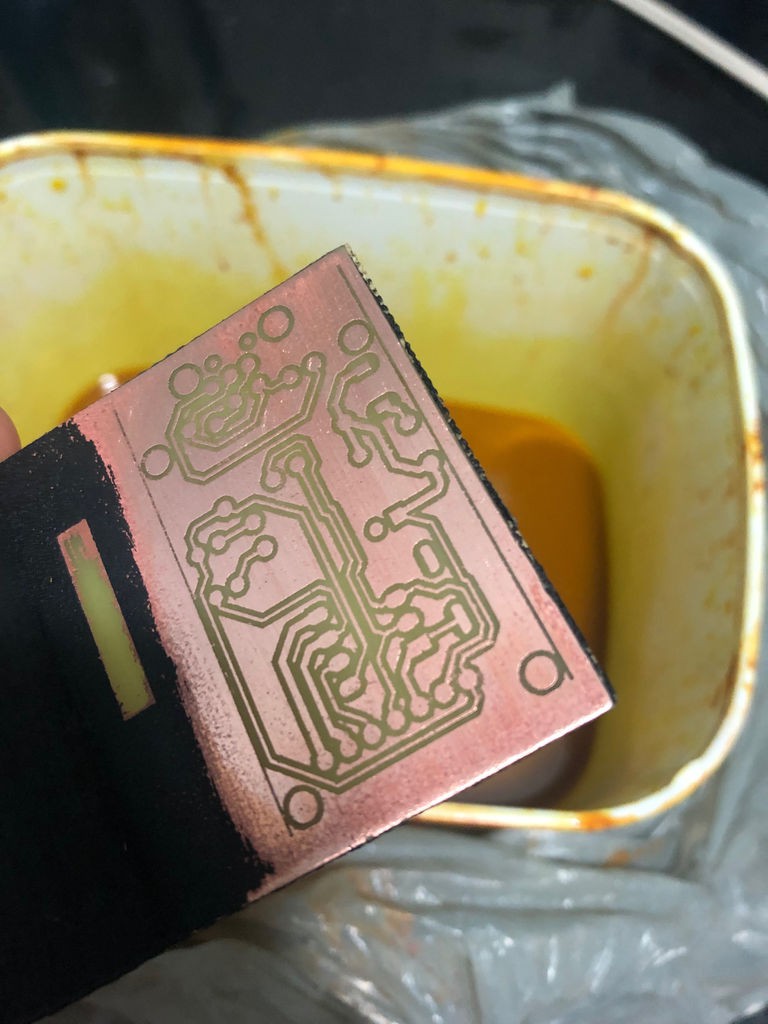
Once the mask is correctly printed on the plate with black traces over the region to be maintained and parts of copper exposed in the tracks to be removed from the plate, the corrosion of the copper should be performed using ferric chloride solution. It takes a few minutes until the material is completely corroded. Check it periodically to make sure that all the material has been removed. In my case, about 5 minutes was enough to remove the material. A little water can be applied over the plate (without applying friction so that the paint is not mechanically removed) for better visualization of the result. It may also be necessary to periodically shake the iron chloride solution to improve the efficiency of the chemical reaction.
![]()
![]()
-
7Mask Removal and Finishing
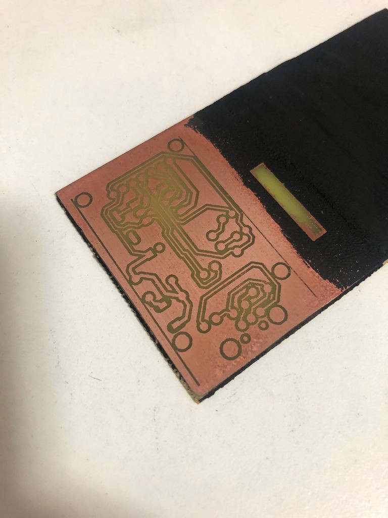
Once the corrosion is complete, the residual mask should be removed. Removal can be done with a brush and running water. Sandpaper can also be used for complete removal of the material, which is faster and can leave a polished finish on the surface.
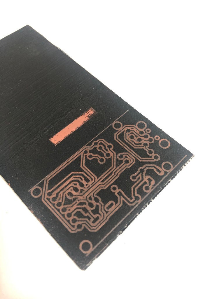
At the end of the process, the board should contain only the copper tracks required for circuit operation. Drill the board (for positioning the components), solder it all and you will have your first printed circuit manufactured using a laser engraver!
As you can see from the photos, it is recommended to cut the board to the proper dimensions before starting the manufacturing. The photos were from my first test, so I didn't mind this before! :p
![]()
-
8End Notes
Thanks for reading my tutorial and watching the video. I hope you liked them and that they would be useful in some way! Do not forget to like and share this project with your friends. Your support is very important! :D
If you still don't follow my tutorials, please take a look at those other projects. I hope you like them!
https://www.instructables.com/id/Joy-Robot-Rob%C3%B4-Da-Alegria-Open-Source-3D-Printed-A/ https://www.instructables.com/id/Wi-Fi-Controlled-Robot-Using-Wemos-D1-ESP8266-Ardu/
https://www.instructables.com/id/Wi-Fi-Voice-Controlled-Robot-Using-Wemos-D1-ESP826/
https://www.instructables.com/id/How-to-17-DOF-Humanoid-Robot/
And if you enjoyed this or other of my tutorials, and want to see more robotics content, Arduino or internet of things, consider financing my future projects! Just bought a kit and feel that it needs a better documentation? Tell me on the comments.
Please consider supporting my future projects with a small donation! :D
- Bitcoin donation: Deposit Address = 1FiWFYSjRaL7sLdr5wr6h86QkMA6pQxkXJ
- Paypal donation: igorfonseca83@gmail.com
- Send me a kit, and I'll create some content on how to assemble it!
Custom PCB Using a Low Power Laser Engraver
In this project it's presented how I used a low power (10W) laser engraver to produce my own homemade custom PCBs!
 igorfonseca83


Discussions
Become a Hackaday.io Member
Create an account to leave a comment. Already have an account? Log In.