-
1RFI filter & protection circuit
The first stage of the circuit is designed to provide a Radio Frequency attenuation and an overloads protection.
For the first purpose a differential low-pass filter capable of remove as much RF energy from the input lines as possible is used. The filter consists of the resistors R1a R1b, and the capacitors C1, C1a, C1b which form a balanced bridge circuit.
The protection circuit is obtained connecting 4 diodes as shown in the LTspice schematic in order to guarantee an adequate protection against damage to the amplifier and the user.
The output of the two electrodes related to the positive and negetive channels must be connected in series with resistors R1a and R1b.
-
2Instrumentation amplifier
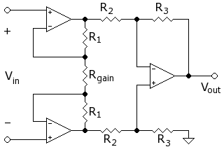
The instumentation amplifier is the most important part of the circuit, it takes 2 voltages as inputs and outputs the difference between the two multiplied by the gain factor. The main features of this component are: very high common mode rejection ratio, very high input impedances, low noise and very low DC offset. Its structure derives from the differential amplifier, with respect to this it has two more op-amp (input buffers) that increase the input impedance and allow the amplification of the differential input signal (Vin) to be varied by varying only one resistor (Rgain).
![]()
In general it is possible to build an instrumentation amplifier by connecting 3 op-amps and 7 resistors as shown in the previous figure, however unless you make it with precision resistors, it will suffer from a low common mode rejection ratio.
For this project I decide to use the INA128 with an appropriate gain resistor Rg in order to obtain an amplification factor G between 10 and 15. It is not convenient to amplify too much because of DC component. However, when I built the circuit I was not yet in possession of the INA128, so I had to adapt by building the in-amp using 3 op-amps as I explained before, I will update the project as soon as I receive the component.
-
3Driven right leg circuit
The purpose of the driven right leg circuit is to feedback any noise from the signal to the body in order to minimize any common mode interference on the body and strengthen the signal.
The third electrode, the one related to the reference ground connection, must be connected to the output of the driven right leg circuit.
-
4High-pass filter
Before amplifying the output signal from the instrumentation amplifier it is advisable to remove the DC component from it. The most convenient way to do this is to use an active high-pass filter by using an op-amp, a resistor R8 and a capacitor C4. The value of R8 and C4 can be tuned in order to obtain a cutoff frequency between 0.1 Hz and 0.01 Hz:
-
5Main amplifier
Once the DC contribution has been removed from the signal, an operational amplifier can be used to amplify it by a factor G tunable by changing the value of R9 and R10, furthermore, by adding a capacitor C5 a low pass filter is obtained through which it is possible to attenuate the high frequencies. It is convenient to set the cutoff frequency between 145 Hz and 165 Hz:
-
6Band-pass filter
A band-pass filter is a combination of a low-pass filter and a high-pass filter, it is able to allow only the passage of those frequencies belonging to the interval established by the upper (fu) and lower (fl) cut off frequencies. The configuration chosen for both the high-pass and the low-pass filters is a two order Sallen-key. Two reasonable intervals for the upper and lower cutoff frequencies could be 90 Hz / 110 Hz and 0.1 Hz / 0.3 Hz, they are both tunable by changing the values of the following resistors and capacitors, according to the laws:
-
7Variable amplifier
The last amplification of the signal is provided by the variable amplifier consisting of the resistances R15, R16 and the variable resistance Rv (0 - 100Kohm):
Is it possible to change the value of G by adjusting the value of the variable resistance Rv
-
8Final conditioning stage
The last part of the circuit is used to make the signal readable by the Arduino Nano board.
The board can only read positive voltages in the range 0 V- 5 V, so it is necessary to adapt the signal "translating it" by adding a DC contribution. For this reason, an inverting adder circuit is used to sum 3 - 4V to the signal and than a inverting stage complete the circuit to "shift" the signal in the wanted voltage range.
-
9Electrodes
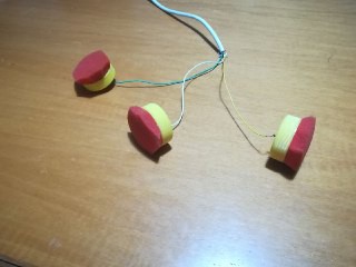
There are different types of electrodes that can be used, the best, but at the same time more expensive, are the active electrodes, which have an internal circuit capable of amplifying the currents increasing the signal quality. In my project I decide to use passive electrodes, in particular salin electrodes.
It is possible to easily build salin electrodes by connecting some sponges containing a solution of saline water to the shielded cables through plastic bottle caps and an aluminum plate, as shown in the following immages:
![]()
![]()
Low-cost EEG circuit
Design and implementation of a low-cost, single-channel, EEG prototype circuit
 Christian Borgia


Discussions
Become a Hackaday.io Member
Create an account to leave a comment. Already have an account? Log In.