 land-boards.com
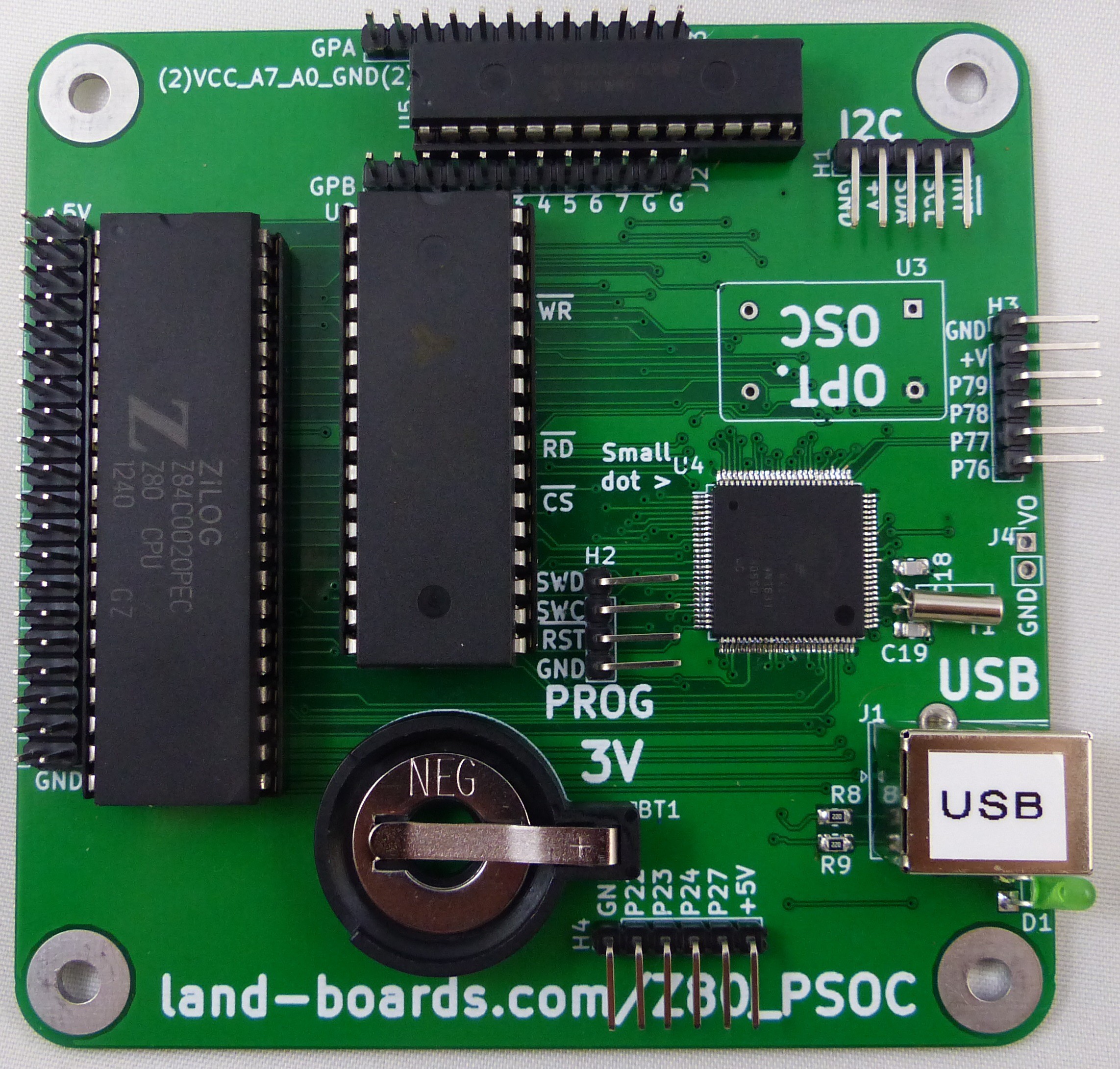
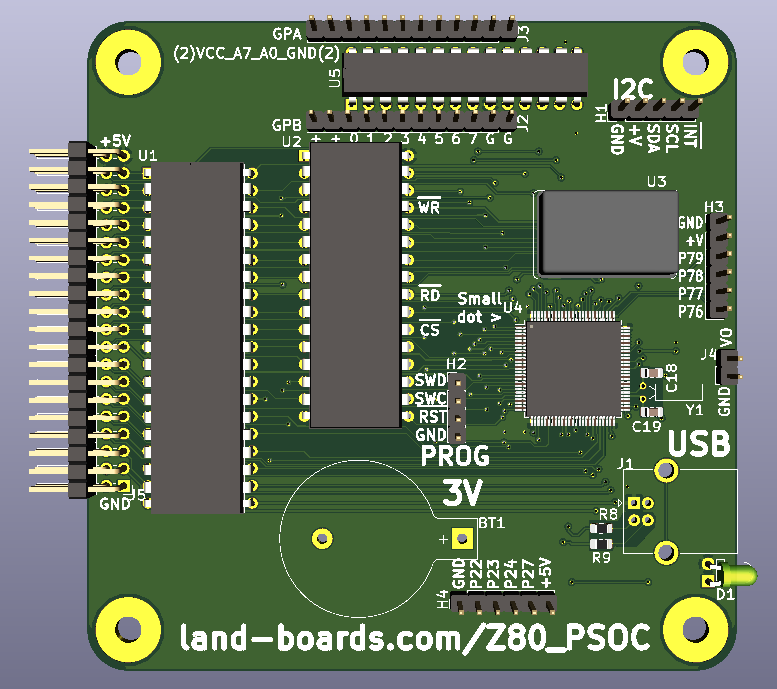
This project uses a Z80, 512KB SRAM and a Cypress Semiconductor (now Infineon) Programmable System on a Chip (PSoC) to make a 3-chip Z80 retro-future computer All of the I/O and SRAM control is performed by the PSoC which emulates Z80 serial and parallel I/O peripherals.
Why Use a PSoC?
The PSoC has the following advantages:
- 5V I/O which lets the PSoC interface directly with the Z80
- Programmable Logic array to implement Z80 glue logic and peripherals
- 32-bit ARM core
- PSoC can download the program to the SRAM so there's no need for EPROM
Schematic
A three chip Z80 design schematic is something like:
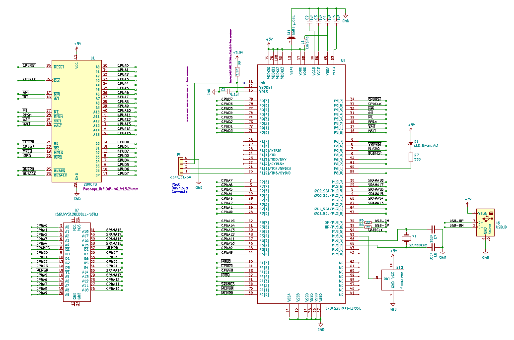
This has three parts - a 512KB SRAM, the Z80 and the PSoC.
The oscillator is optional unless precise serial connections are required. This is not necessary in most applications since the PSoC has a USB interface.
The PSoC emulates the control/status registers of a 6850 ACIA.
Options
Additional parallel I/O is via an optional MCP23017 chip which connects to I2C pins on the PSoC. This is slower than a PIO chip, but probably still OK for most applications. This is similar to the Z80-MBC2 board without requiring the complications of the ATMEGA interface. In that design, the ATMEGA interfaces to the CPU force feeding it instructions with boot sequences. And this is one less IC.
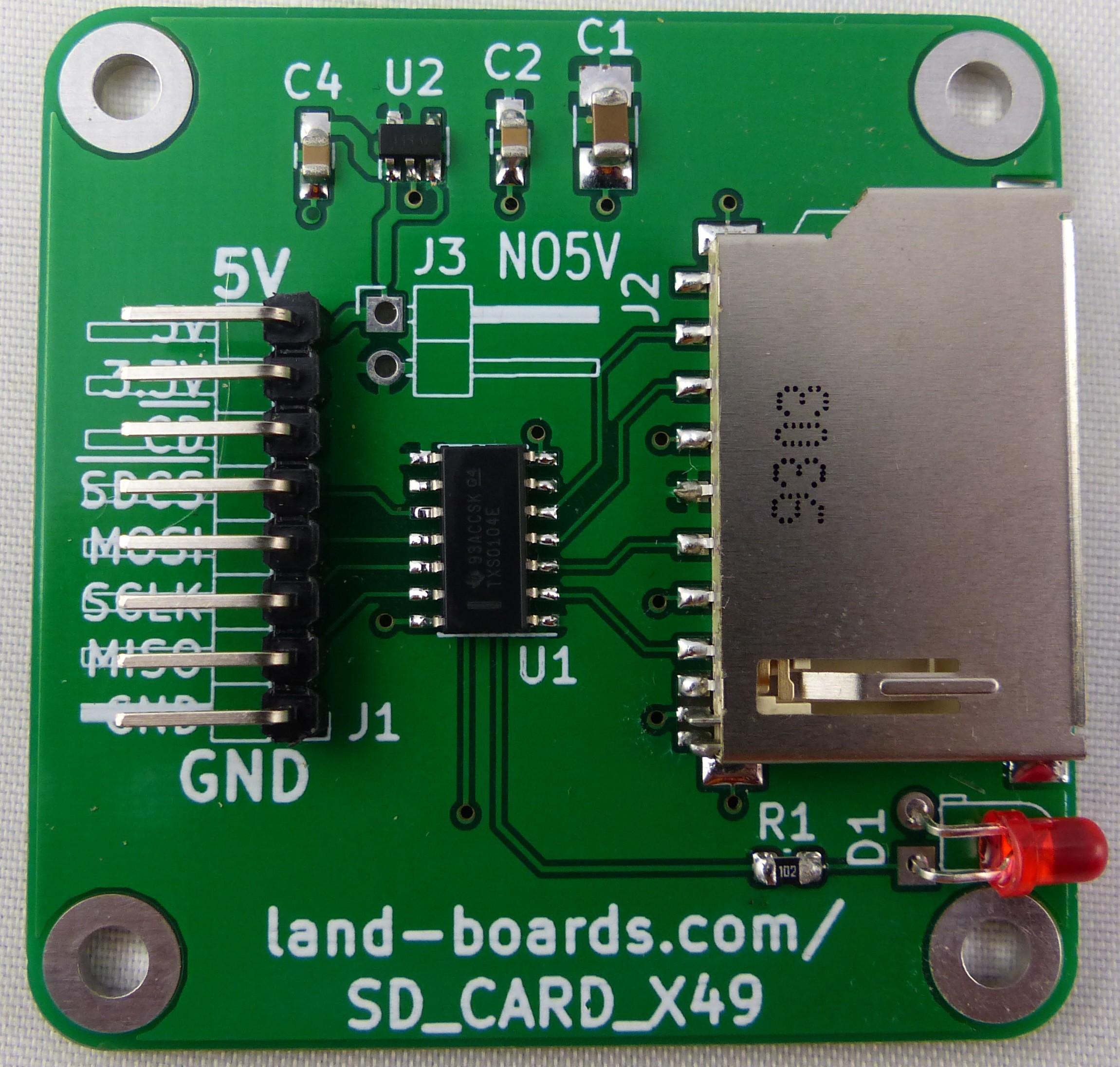
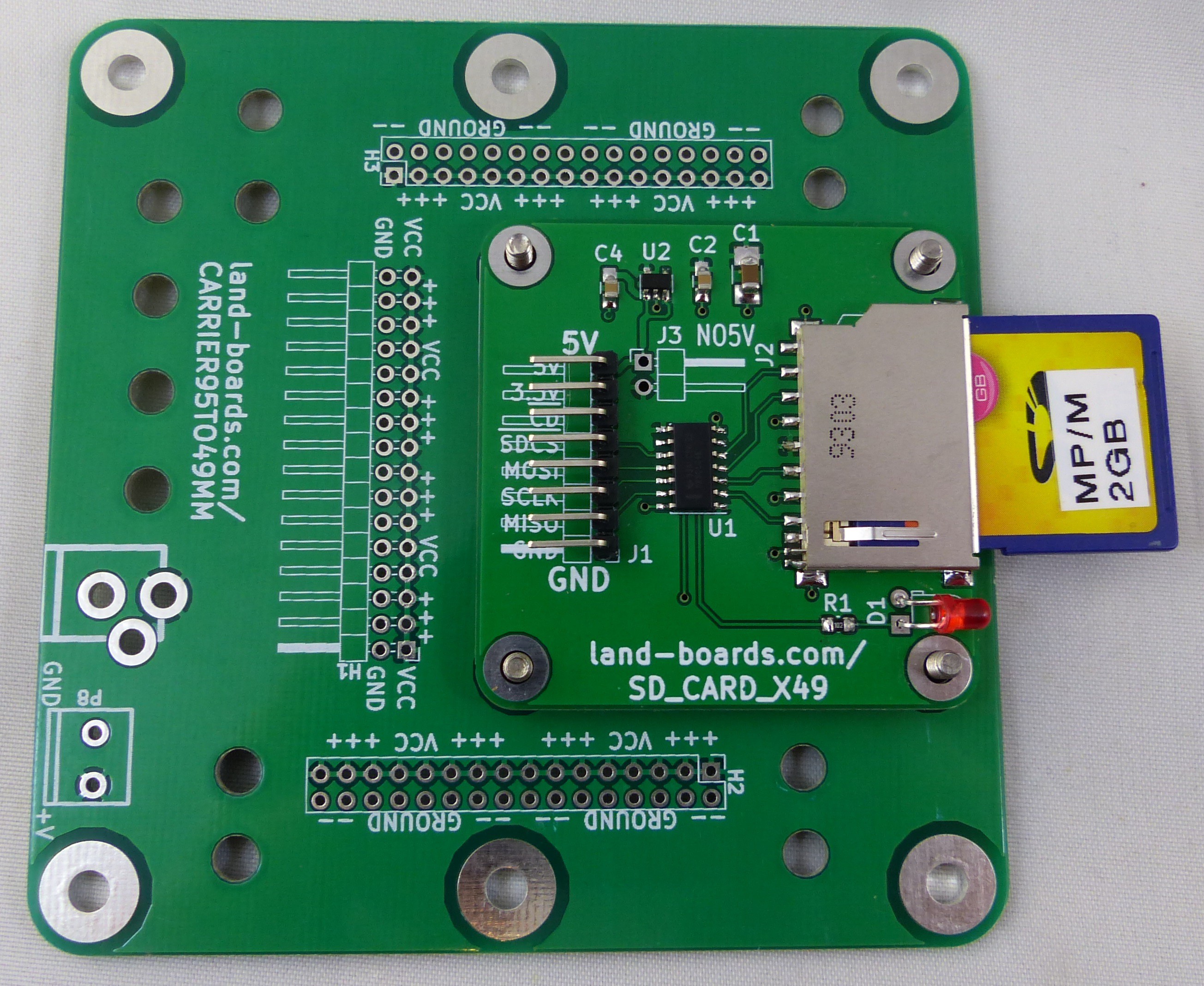
The PSoC SPI interface connects to an optional external SD card.
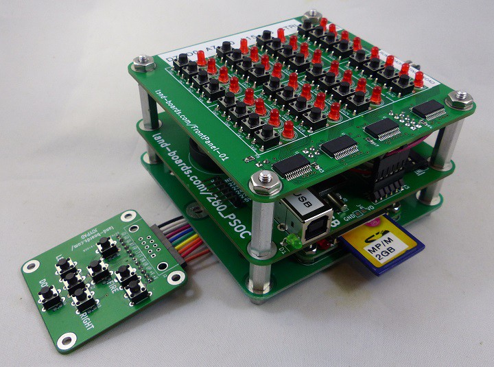
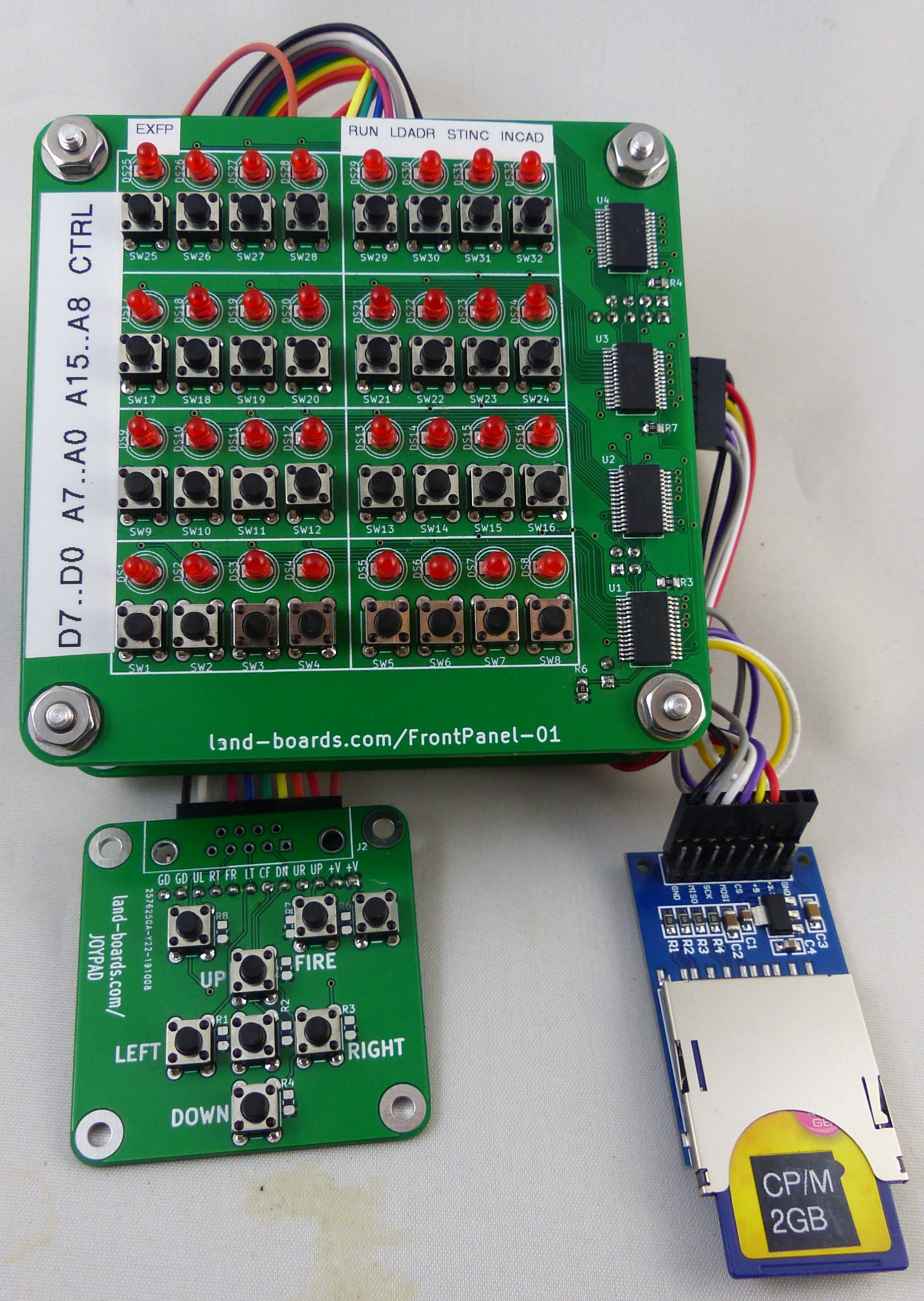
An optional Front Panel card was also created which connects via I2C to the PSoC.
Booting Software Builds
In this design, the PSoC downloads the software to the SRAM and takes the Z80 out of reset. Hardware/software implementations which have both EPROM and RAM could be "emulated" by banking the SRAM. Control of upper RAM address bits allows a bank of the SRAM to work as an EEPROM. The program can be downloaded from the emulated SRAM into the SRAM itself.
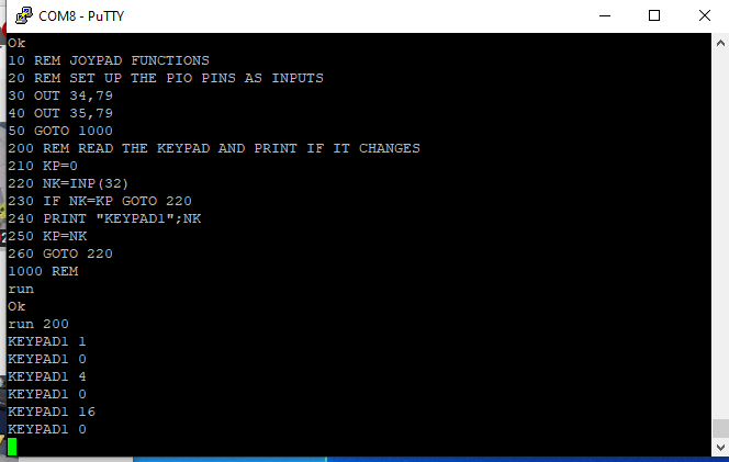
512KB MultiOS Multicomp
Card runs CP/M 2.2, CP/M 3.0, BASIC.
Z80 Peripheral Emulation
The Z80 peripherals are emulated insider the PSoC - mostly in hardware. For instance, the DART/SIO consist of data and control/status registers which are I/O mapped to the Z80 and memory mapped to the PSoC. An 8-bit mailbox interfaceis used for all peripherals and the I/O address is latched in a register in the PSoC.
Counter/Timers could also easily be simulated in PSoC hardware.
The PCB would be less expensive (than my previous design) since it could easily be built in a board that is smaller (95x95mm which is the sweet spot for PCB costs. PCBWay or JLCPCB wants $14 for 10 boards that are larger than 100x100mm but only $5 for 10 boards which are less than 100x100mm or less.
Design Logs
See the 90+ logs here for the card which provide excruciating details on the design process.
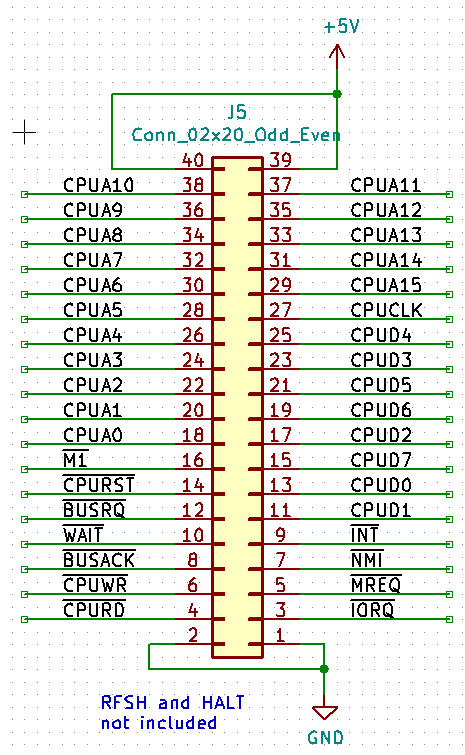 Most of the signals are directly from the Z80. Some of them are hard driven from the PSoC and would need to be changed to Open Drain outputs with pull-ups if there was an expansion card attached to this connector. I mostly want the connector to aid in debugging. Getting all those little chip clips on the Z80 pins and making them stay is just too hard. It's much easier to push the female pin from the Logic Analyzer onto a header.
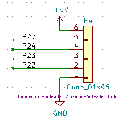
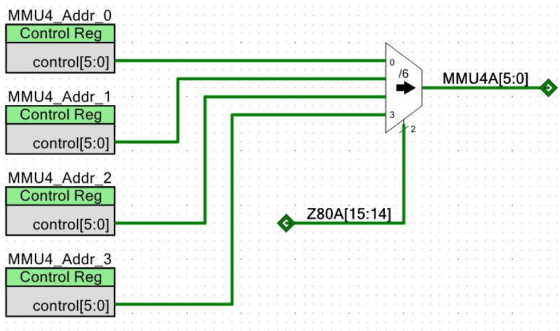
 The current page that drives the MMU1 gets changed to go through the new level of multiplexer. My assumption is that PSOC Creator will reduce the logic automatically.
 The HEX file from Multiboot Multicomp gets converted into a C array with srec_cat as previously done and added to the project. The Z80 IO handler gets updated to add handlers for the new Memory Mapper. The Harware_Config.h file gets updated to add the new Memory Map (USING_MEM_MAP_4) and top level design (MULTIBOOT_CPM). This is very similar to the 9-Chip CP/M design described in a previous blog.
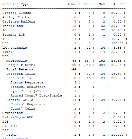
 Noah
Noah
 Ted Fried
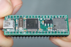
 David Viens
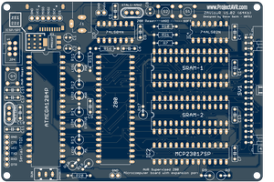
 Steve Smith
Nice, I did pretty similar design with PSoC 4200L and Signetics 2650 some time ago http://www.8bity.cz/2019/signetics-2650-baby-system-trochu-jinak-s-psoc-4200l/