land-boards.com
-
Updates to Boot Menu on PSoC
09/17/2022 at 14:23 • 0 commentsIt's been a while. I plugged in the board USB and forgot how to run it. I even forgot which button I needed to press on the front panel to get Multiboot to run. This Hackaday page helped me remember. Glad I made it.
Decided to add hints to the PSoC monitor menu. Got a bit carried away but it's really easy now.
The PSoC now boots to the following screen showing what the Front Panel buttons do:
Z80_PSoC - Running Front Panel

SW25 SW26 SW27 SW28 SW29 SW30 SW31 SW32
Run  Mon  N/A  N/A  N/A  LDAD STOR INCA

SW17 SW18 SW19 SW20 SW21 SW22 SW23 SW24
A15  A14  A13  A12  A11  A10  A9   A8

SW9  SW10 SW11 SW12 SW13 SW14 SW15 SW16
A7   A6   A5   A4   A3   A2   A1   A0

SW1  SW2  SW3  SW4  SW5  SW6  SW7  SW7
D7   D6   D5   D4   D3   D2   D1   D0

Press SW25 (upper left button) to exit Front Panel and run Z80
Press SW26 to run Monitor/Test Code
Pressing the upper left button on the Front Panel (SW25) goes directly to Multiboot.
The next button in boots the monitor. The monitor looks like:
Land Boards, LLC - Z80_PSoC monitor
I - Initialize SD Card
B - Blink LED
F - Read Front Panel
Rxxxxxxxx - Read sector xxxxxxxx from the SD Card
N - Read next sector from the SD Card
W - Write to the SD Card at 2GB - 1 sector
X - eXit Monitor and run Z80
? - Print this menu
Pressing X goes to Multiboot.
The PSoC waits until the USB terminal (PuTTY) is running. Now I feel like I could plug the card in anytime and just use it. Added P-Touch labels to SW25, SW26 to remind me what they do.
Also noted that the USB Serial port can be set to any baud rate since the PSoC automatically adjusts. Tried 230.4 kb and it worked just fine.
-
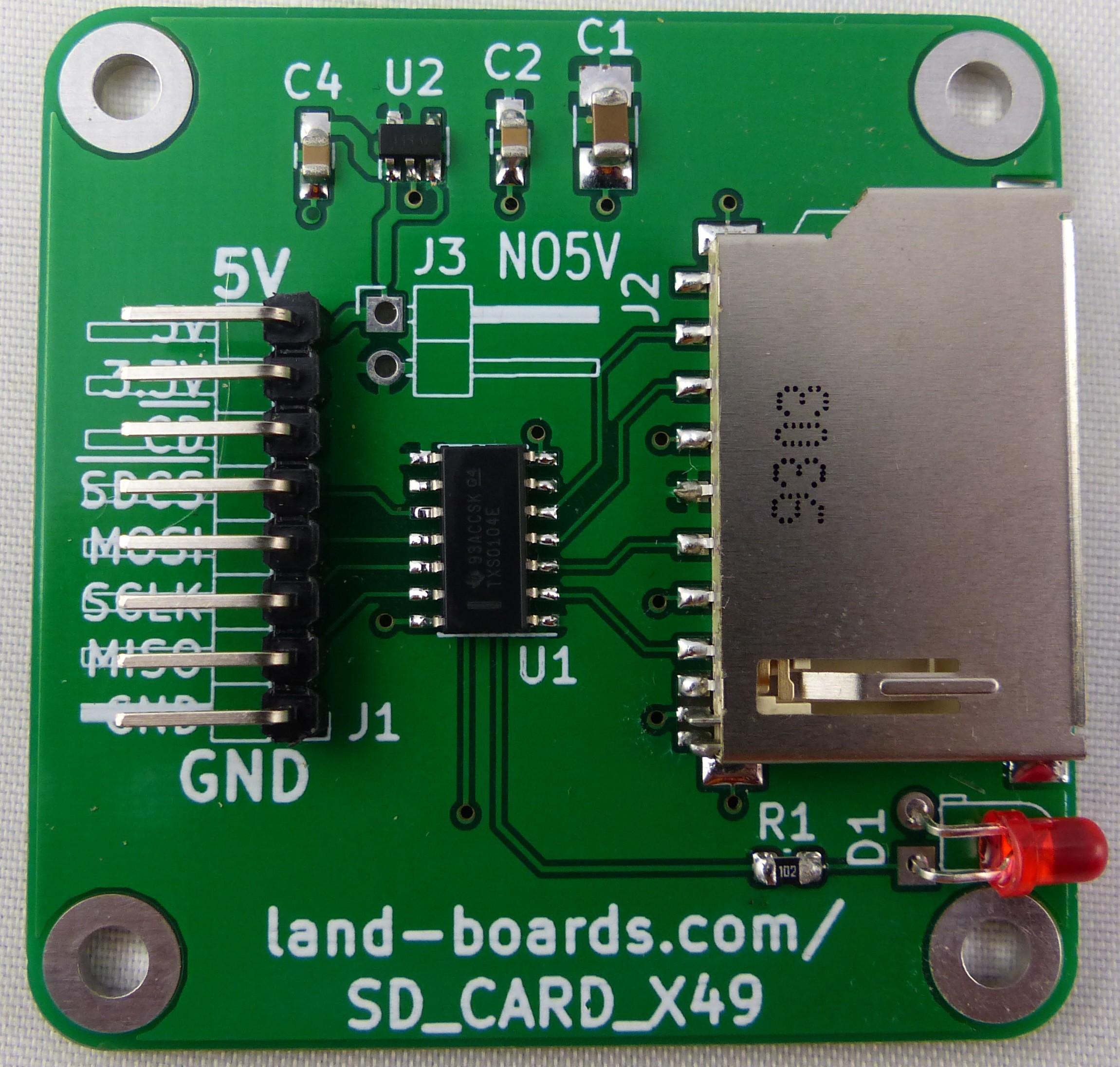
SD Card Adapter
02/21/2020 at 14:34 • 0 commentsMade my own SD Card adapter to use with my Z80_PSOC card. Works great. Made this card because I wanted good mounting holes. Also, didn't like the series resistor method of shifting the 5V of the Z80_PSOC to 3.3V of the SD Card that most cards use in their design
![]()
Here's the SD Card. Uses a TXS0104E level shifter to convert the 5V of the Z80 to the 3.3V used by the SD Card.
![]()
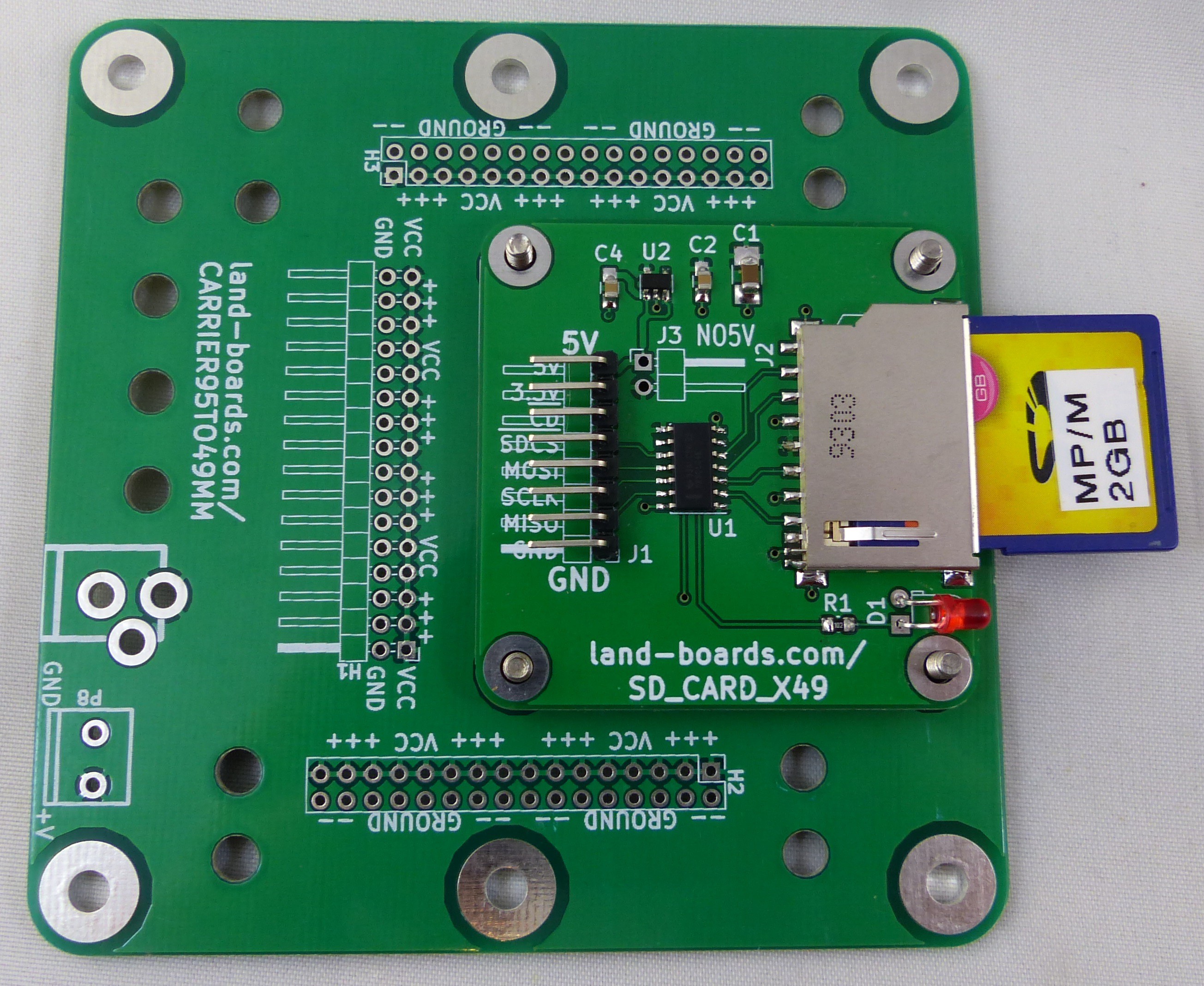
Here's the card mounted to a carrier which lets it stack up with the other 95x95mm cards.
![]()
-
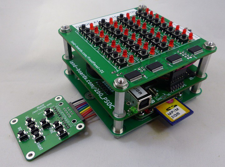
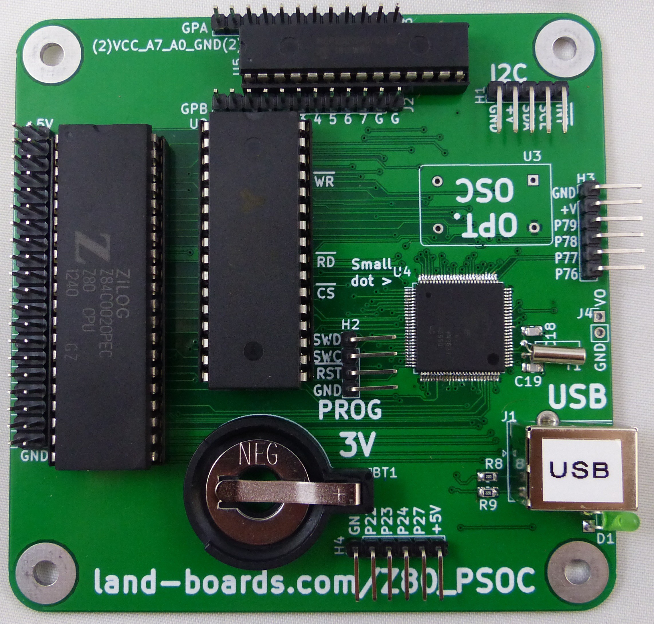
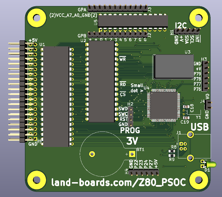
Pics of New Board
12/08/2019 at 17:57 • 0 commentsHere is a picture of the new Rev 3 card. The card runs fine and there are no wires.
![]()
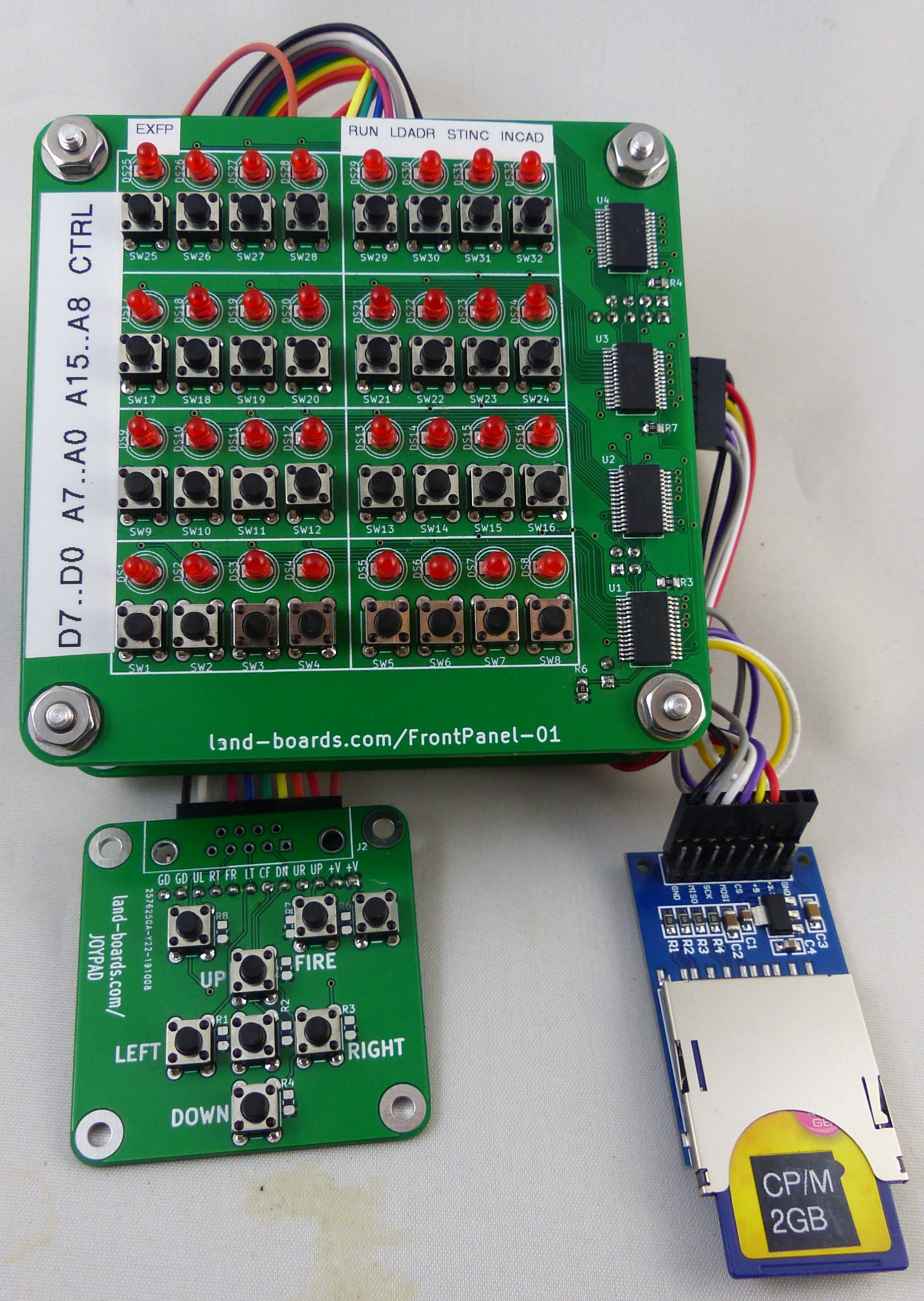
Here's the stackup with the Front Panel, JoyPad and SD Card.
![]()
-
New Board Spin
12/04/2019 at 14:25 • 0 commentsThere were some things I wanted to add/change on the first rev of the card. Got the PCBs back from PCBs fabrication but haven't assembled the cards yet. This change:
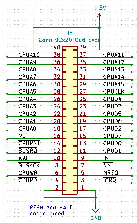
- Adds Z80 expansion connector (J5)
- Fixes labeling on the Programming connector (H2)
- Adds control signal labels for SRAM debugging (WR*, RD*, and CS*)
- Adds a pin 1 indicator for the PSoC "Small dot >" (at U4)
- Adds I/O Connector (H4)
- Rotate I2C connector to allow horizontal header to be used
- Might want to use right angle connectors at J4, H2, H3, and H4
Z80 Bus Expansion Connector
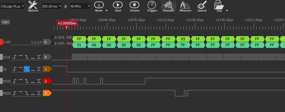
The primary feature added is the 40-pin bus expansion connector which brings out the Z80 bus. Here's the connector pinout:Most of the signals are directly from the Z80. Some of them are hard driven from the PSoC and would need to be changed to Open Drain outputs with pull-ups if there was an expansion card attached to this connector. I mostly want the connector to aid in debugging. Getting all those little chip clips on the Z80 pins and making them stay is just too hard. It's much easier to push the female pin from the Logic Analyzer onto a header.
H4 I/O Connector
Also added a 6-pin connector for additional I/O (maybe an RS-232 port?). Pxx are PSoC pins. -
Front Panel Card Change
11/19/2019 at 12:38 • 0 commentsRemoved the straight connector for I2C and replaced it with a dual row right angle connector. One of the pins is deliberately left out on the 2x5 connector. That is because other cards that connect to the I2C bus won't use the same interrupt line as the Front Panel.
This provides a more robust connection to the Front Panel card. It is less likely to come loose and provides additional clearance down to card below (Z80_PSOC card).
Also, took apart the staggered stack-up and rebuilt it using 1/4" standoffs that are #6-32 M-F parts for the standoffs below the Z80_PSOC CPU card. Using 1" standoffs between the Front Panel and CPU cards and used #6-32 nuts at the top of the Front Panel Card. This makes the entire stackup less than 1-1/2" tall with buttons and switches at the top of the stack (Picture with taller standoffs at the bottom).
The SD Card and JoyPad cards are cabled out to external cards. Going to make a 49x49mm card which has an SD card socket. The SD card will be used with a 95x95mm to 49x49mm adapter card which will allow the SD card to be stacked easily in a mechanically sound manner. The SD card can have a right angle connector and will be routed to the Z80_PSOC CPU card. The card could be mounted on the bottom of the 95-49mm adapter card so that the cable route down but then the I2C cable from the Front Panel to the Z80_PSOC card would route down around the card. Another possibility is making a version of the adapter card with a slot on the side for cable routing.
-
Multi-boot Multicomp (Part 3)
11/16/2019 at 20:07 • 0 commentsIn the last log we got the Multi-boot monitor to run however, when BASIC was run it hung.
The Z80 is trying to access I/O address 0x39 which isn't implemented yet. That's the swap back to the original BIOS code. Since it was never swapped out it can be swapped right back in with an ackIO( ).
After adding back in the BIOS, BASIC now works as launched from Multi-boot with the S5 command.
Cold or Warm?

Memory top?
Z80 BASIC Ver 4.7b
Copyright (C) 1978 by Microsoft
57694 Bytes free
Ok

10 print "HI"
run
HI
Ok
list

10 PRINT "HI"
Ok
Added in code that when the 0x39 (swapped back) is received then goes and causes a BUSREQ*, waits for a BUSACK* and copies the BIOS back into SRAM.
Back to Debugging CP/M
The CP/M code is in and the BIOS code looks like this:
; Disable the ROM, pop the boot disk and IOBYTE from the stack
; (supplied by monitor), then start the OS
;    org 0FFB0h
popAndRun:
    ld A,01h
    out (38h),A        ; kick ROM

    pop AF            ; Monitor gives physical boot volume
    ld (mnttab),A        ; ignore 8 bit volume number

    pop AF            ; Monitor gives the IOBYTE ...
    ld (IOBYTE),A


    ld HL,mnttab
    ld (0FFFEh),HL        ; put mounttab vector in FFFE
    ld HL,backdoor
    ld (0FFFCh),HL        ; put backdoor vector above that
    ld A,0C3h
    ld (0FFFBh),A        ; and a JP opcode above that
    ld C,0
    jp BIOS
S2 also works.
Z80 CP/M BIOS 2.20
Based on MULTICOMP by G. Searle 2007-13
http://searle.hostei.com/grant/Multicomp

CP/M 2.2 (c) 1979 by Digital Research


STARTUP?

A>dir
A:   Volume 002 : ASM      COM : DDT      COM : DISPLAY  COM
A: DOWNLOAD COM : DUMP     COM : DUTIL    COM : ED       COM
A: LOAD     COM : MOUNT    COM : PIP      COM : RDINIT   COM
A: RESET    COM : STAT     COM : SUBMIT   COM : TIME     COM
A>
S3 also works.
CP/M V3.0 Loader
Copyright (C) 1998, Caldera Inc.

 BNKBIOS3 SPR  FA00  0600
 BNKBIOS3 SPR  7400  0C00
 RESBDOS3 SPR  F400  0600
 BNKBDOS3 SPR  4600  2E00

 61K TPA


CP/M Version 3.0 BIOS (2016/9/13)
FPGA-Z80 Multicomputer
Original concept by Grant Searle


A>
S4 boots but hangs.
MP/M II V2.1 Loader
Copyright (C) 1981, Digital Research
Nmb of consoles     =  4
Breakpoint RST #    =  6
Memory Segment Table:
SYSTEM  DAT  FF00H  0100H
TMPD    DAT  FE00H  0100H
USERSYS STK  FC00H  0200H
XIOSJMP TBL  FB00H  0100H
RESBDOS SPR  EF00H  0C00H
XDOS    SPR  CD00H  2200H
BNKXIOS SPR  C200H  0B00H
BNKBDOS SPR  9F00H  2300H
BNKXDOS SPR  9D00H  0200H
TMP     SPR  9900H  0400H
LCKLSTS DAT  9600H  0300H
CONSOLE DAT  9200H  0400H
-------------------------
MP/M II Sys  9200H  6E00H  Bank 0
Memseg  Usr  0000H  C000H  Bank 1
Memseg  Usr  0000H  C000H  Bank 2
Memseg  Usr  0000H  C000H  Bank 3
Memseg  Usr  0000H  C000H  Bank 4
Memseg  Usr  0000H  C000H  Bank 5
Memseg  Usr  0000H  C000H  Bank 6
Memseg  Usr  0000H  9200H  Bank 0
S6 doesn't boot.
S7 boots.
> S7
CP/M V3.0 LoaderBIOS for Grant Searle's Multicomputer

 Loading ZPM3...
 BNKBIOS3 SPR  FA00  0600
 BNKBIOS3 SPR  7400  0C00
 RESBDOS3 SPR  F400  0600
 BNKBDOS3 SPR  4600  2E00

 61K TPA

CP/M Version 3.0 BIOS (2016/9/13)
FPGA-Z80 Multicomputer
Original concept by Grant Searle

    ZCPR compatible system for CP/M+ by Simeon Cran

Loading NAMES.NDR

RamDisk: Initialized

00:00 A0:SYS>
Tried S1 twice and it booted on the second try.
Z80 CP/M BIOS 2.20
Based on MULTICOMP by G. Searle 2007-13
http://searle.hostei.com/grant/Multicomp

Dos+ 2.5  Copyright 1986 (c) by C.B. Falconer

CCP+ Ver. 2.2

A>
zexall runs on S1.
A>A:DOWNLOAD zexall.com
................................................................
....
OK

A>zexall
Z80 instruction exerciser
<adc,sbc> hl,<bc,de,hl,sp>....  OK
add hl,<bc,de,hl,sp>..........  OK
add ix,<bc,de,ix,sp>..........  OK
add iy,<bc,de,iy,sp>..........  OK
aluop a,nn....................  OK
aluop a,<b,c,d,e,h,l,(hl),a>..  OK
aluop a,<ixh,ixl,iyh,iyl>.....  OK
aluop a,(<ix,iy>+1)...........  OK
bit n,(<ix,iy>+1).............  OK
bit n,<b,c,d,e,h,l,(hl),a>....  OK
cpd<r>........................  OK
cpi<r>........................  OK
<daa,cpl,scf,ccf>.............  OK
<inc,dec> a...................  OK
<inc,dec> b...................  OK
<inc,dec> bc..................  OK
<inc,dec> c...................  OK
<inc,dec> d...................  OK
<inc,dec> de..................  OK
<inc,dec> e...................  OK
<inc,dec> h...................  OK
<inc,dec> hl..................  OK
<inc,dec> ix..................  OK
<inc,dec> iy..................  OK
<inc,dec> l...................  OK
<inc,dec> (hl)................  OK
<inc,dec> sp..................  OK
<inc,dec> (<ix,iy>+1).........  OK
<inc,dec> ixh.................  OK
<inc,dec> ixl.................  OK
<inc,dec> iyh.................  OK
<inc,dec> iyl.................  OK
ld <bc,de>,(nnnn).............  OK
ld hl,(nnnn)..................  OK
ld sp,(nnnn)..................  OK
ld <ix,iy>,(nnnn).............  OK
ld (nnnn),<bc,de>.............  OK
ld (nnnn),hl..................  OK
ld (nnnn),sp..................  OK
ld (nnnn),<ix,iy>.............  OK
ld <bc,de,hl,sp>,nnnn.........  OK
ld <ix,iy>,nnnn...............  OK
ld a,<(bc),(de)>..............  OK
ld <b,c,d,e,h,l,(hl),a>,nn....  OK
ld (<ix,iy>+1),nn.............  OK
ld <b,c,d,e>,(<ix,iy>+1)......  OK
ld <h,l>,(<ix,iy>+1)..........  OK
ld a,(<ix,iy>+1)..............  OK
ld <ixh,ixl,iyh,iyl>,nn.......  OK
ld <bcdehla>,<bcdehla>........  OK
ld <bcdexya>,<bcdexya>........  OK
ld a,(nnnn) / ld (nnnn),a.....  OK
ldd<r> (1)....................  OK
ldd<r> (2)....................  OK
ldi<r> (1)....................  OK
ldi<r> (2)....................  OK
neg...........................  OK
<rrd,rld>.....................  OK
<rlca,rrca,rla,rra>...........  OK
shf/rot (<ix,iy>+1)...........  OK
shf/rot <b,c,d,e,h,l,(hl),a>..  OK
<set,res> n,<bcdehl(hl)a>.....  OK
<set,res> n,(<ix,iy>+1).......  OK
ld (<ix,iy>+1),<b,c,d,e>......  OK
ld (<ix,iy>+1),<h,l>..........  OK
ld (<ix,iy>+1),a..............  OK
ld (<bc,de>),a................  OK
Tests complete
CCP+ Ver. 2.2
A>
-
Multi-boot Multicomp (Part 2)
11/14/2019 at 15:45 • 0 commentsI've got the BIOS loading for Multi-boot Multicomp. It boots up to the Multi-boot prompt.
>
  Available Commands:

  :ccxxxxiibbbbbb Load Intel-Hex file record
  Rxxxx           Run from address xxxx
  Sddd            System boot
  Iddd            Init: Format directory
  Pddd[,xxxx]     PutSys: write system image[,loadaddress]
                  (No address: re-use last loadaddress)
  Gddd[,xxxx]     GetSys: load system track

  Dxxxx[,yyyy]  Dump memory from xxxx [,to yyyy]
                D (no address) shows next block
  Cxxxx         Change/show memory at xxxx
                CR advances "," quits

  ddd is a decimal volume number,
  xxxx, yyyy is a hexadecimal address.
  Leading zeros may be omitted.
  ESC or ^C aborts.

>
When I enter "S1" it hangs. I single stepped through the SD code from the PSoC side and it looks like the SD card is working the same as Grant's CP/M boot (build tested earlier).
At the least the PSoC is not hung but there's no more I/O requests from the Z80.
Bank Switching vs MMU
The previous CP/M design does a bank switch with a write to I/O address 0x38. There is no bank switching with the MMU so it's not the case that it needs to swap out the banks. But I'm not sure what the effect of not having an actual EPROM would be in this case. The BIOS gets loaded into the first 2K of SRAM.
The FPGA version of this design had two addresses for switching ROM and SRAM in/out of the first 2KB. That could be done in this instance by re-copying the monitor program into the SRAM, but probably is unnecessary. There's also no writes in the BIOS to the switching although there has to be something somewhere in the code to do the switching otherwise the bottom 2KB would not be accessible. This command won't work:
When you type "reset" you enact a cold reset,
returning you to the ROM monitor.
SYSRUN Routine
The SYSRUN routine is short:
; SYSRUN - boot (load and run) from system track of selected volume
;-------------------------------------------------------------
sysrun:    call getargs   ; get volume and loadaddress
    call setDskIO
    call readsys          ; read disk contents to loadaddress
    call getlen           ; find loadaddress and length
    ldir                  ; move buffer to image
    ld A,(aciaCtl)        ; message bootdisk and console to
    and 02h               ; main program - 2 methods, on stack
    rrca                  ; and in alternate BC registers
    xor 01h               ; convert to iobyte...
    push AF               ; ...to save bytes in BIOS
    ld C,A
    ld A,(volume)         ; tell BIOS which is ...
    push AF               ; ...the active bootvolume
    ld B,A
    exx                   ; also make b'=bootdisk, c'=console
    ld HL,(0FFFEh)        ; pop and run location
    jp (HL)               ; bye bye
Limited Ability to Monitor Z80 Activity
It's a pain to hook up the logic analyzer to the Z80. Rev 3 of this board will make it much easier because it brings out all Z80 signals to a 40 pin header.
All of these signals already go to the Z80. It would be nice to be able to break into the PSoC monitor and single step through Z80 code or at least capture the address/data of the bus.
Stuff I Tried
Also tried G1,4000 to read the SD card for image 1 into memory at 0x4000. It hung PuTTY.
- Command G performs the same service, but stops when the
image is loaded and returns to the monitor prompt.
This command is useful to examine the image,
or prepare it for loading onto a volume.
I am able to Change and Dump memory which makes me conclude that the MMU must be functioning correctly.
> C4000
4000 00 40
4001 01 00
> C8000
8000 00 80
8001 01 00
> CC000
C000 00 C0
C001 01 00
> D4000
4000  40 00 02 03 04 05 06 07 08 09 0A 0B 0C 0D 0E 0F       @...............
> D8000
8000  80 00 02 03 04 05 06 07 08 09 0A 0B 0C 0D 0E 0F       ................
> DC000
C000  C0 00 02 03 04 05 06 07 08 09 0A 0B 0C 0D 0E 0F       @...............
SD Card Sector Map
S1 attempts to load sector 0x4000.
Card layout:
sector  --------------------------------------------------------------
0       the first 8 Mbytes unused:  \    Put partition table here
16384   8MB volume 1                |    if desired.
32768   8MB volume 2                |
49152   8MB volume 3                |
        =    .                      |
        =    .                      | 2 Gbyte maximum reserved memory
1949696 end of 1 GB card, or        |
        =    .                      |
        =    .                      |
4161536 8MB volume 254 (RAMDISK)    |
4177920 8BM left unused (disk -1)   /
4194304 unused space to be formatted as FAT partition
------------------------------------------------------------
16384 dec = 0x4000
Logic Analyzer shows 0xFF in the sector.
Put the SD card into the MultiComp RETRO-EP4CE6 card and it worked so it seems like the card itself is OK.
Not sure if this it doesn't work in this card because the SD card is an SDHC card? Could try this image on an SD card (non-SDHC). Put the image onto a 2 GB card. Didn't boot but this did work:
Read sector from the SD Card
Sector: 0x4000
0000  c3 5c e3 c3 5f e3 7e 00 00 00 00 00 00 00 00 00  .\.._.~.........
0010  00 00 00 00 00 00 20 20 43 43 50 2b 20 76 32 2e  ........CCP+.v2.
0020  32 20 28 43 29 20 31 39 38 36 2c 20 43 2e 42 2e  2.(C).1986,.C.B.
0030  20 46 61 6c 63 6f 6e 65 72 2c 20 54 65 6c 2e 20  .Falconer,.Tel..
0040  28 32 30 33 29 20 32 38 31 2d 31 34 33 38 2c 20  (203).281-1438,.
0050  36 38 30 20 48 61 72 74 66 6f 72 64 20 54 70 6b  680.Hartford.Tpk
0060  2e 2c 20 48 61 6d 64 65 6e 2c 20 43 54 2e 2c 20  .,.Hamden,.CT.,.
0070  55 53 41 00 00 00 00 00 00 00 00 00 00 00 00 00  USA.............
0080  00 00 00 00 00 00 00 00 4e 6f 20 46 69 6c 65 00  ........No.File.
0090  4e 6f 20 72 6f 6f 6d 00 41 6c 6c 20 28 79 2f 4e  No.room.All.(y/N
00a0  29 3f 00 46 69 6c 65 20 65 78 69 73 74 73 00 4e  )?.File.exists.N
00b0  6f 20 55 50 53 48 49 46 54 00 2a fa e7 b7 c8 3d  o.UPSHIFT.*....=
00c0  d6 10 29 3c 20 fc c9 fe 61 d8 fe 7b d0 e6 5f c9  ..)<....a..{.._.
00d0  fe 30 d8 fe 3a 3f c9 3e 0d cd de e0 3e 0a d5 5f  .0..:?.>....>.._
00e0  3e 02 cd 74 e1 d1 c9 fe 0a 38 11 c5 0e 2f 0c c6  >..t.....8.../..
00f0  f6 38 fb c6 0a f5 79 cd de e0 f1 c1 c6 30 18 de  .8....y......0..
0100  3e 0b cd 74 e1 c8 3e 01 18 6a af 32 dc e7 11 bc  >..t..>..j.2....
0110  e7 3a f7 e7 17 38 10 1a b7 20 0c cd 27 e1 c0 3c  .:...8......'..<
0120  12 cd 27 e1 c0 12 c9 3e 0f cd 74 e1 3c c9 3e 10  ..'....>..t.<.>.
0130  18 f7 3e 12 18 f3 11 bc e7 3e 11 18 ec 3e 13 18  ..>......>...>..
0140  e8 11 bc e7 3e 14 18 2c 3e 15 18 28 3e 16 18 d9  ....>..,>..(>...
0150  11 80 00 3e 1a 18 1d 3e 19 18 19 ed 4b bb e7 79  ...>...>....K..y
0160  b7 fc 6c e1 4f ed 43 bb e7 5f 18 02 1e ff 3e 20  ..l.O.C.._....>.
0170  18 02 3e 0d e5 d5 c5 dd e5 4f cd 05 00 b7 dd e1  ..>......O......
0180  c1 d1 e1 c9 3a 98 e7 cd 69 e1 11 99 e7 cd 27 e1  ....:...i.....'.
0190  28 27 d5 3a a8 e7 3d 32 b9 e7 11 07 e0 cd 53 e1  ('.:..=2......S.
01a0  d1 cd 44 e1 20 13 32 86 e0 21 a7 e7 77 23 35 cd  ..D...2..!..w#5.
01b0  2e e1 28 05 cd 00 e1 28 10 3a 98 e7 cd 69 e1 11  ..(....(.:...i..
01c0  99 e7 cd 3d e1 af 32 ba e7 cd 50 e1 3a 04 00 f5  ...=..2...P.:...
01d0  07 07 07 07 e6 0f cd 69 e1 f1 e6 0f 5f e5 2a f8  .......i...._.*.
01e0  e7 cd c0 e0 e1 da 3d e3 3e 0e 18 88 3a ba e7 b7  ......=.>...:...
01f0  c4 84 e1 3a 04 00 f5 e6 0f c6 41 cd de e0 f1 07  ...:......A.....
This makes sense since my SD card code doesn't support SDHC Cards. Seems like I could determine what sort of card is attached and use the right command for SDHC cards.
Still not sure why it didn't run when I did S1.
One good sign, G1 worked.
> G1
System Read OK
>
It looks like this loaded correctly.
> DE000
E000  C3 5C E3 C3 5F E3 7E 00 00 00 00 00 00 00 00 00       C\cC_c~.........
E010  00 00 00 00 00 00 20 20 43 43 50 2B 20 76 32 2E       ......  CCP+ v2.
E020  32 20 28 43 29 20 31 39 38 36 2C 20 43 2E 42 2E       2 (C) 1986, C.B.
E030  20 46 61 6C 63 6F 6E 65 72 2C 20 54 65 6C 2E 20        Falconer, Tel.
E040  28 32 30 33 29 20 32 38 31 2D 31 34 33 38 2C 20       (203) 281-1438,
E050  36 38 30 20 48 61 72 74 66 6F 72 64 20 54 70 6B       680 Hartford Tpk
E060  2E 2C 20 48 61 6D 64 65 6E 2C 20 43 54 2E 2C 20       ., Hamden, CT.,
E070  55 53 41 00 00 00 00 00 00 00 00 00 00 00 00 00       USA.............
> D
E080  00 00 00 00 00 00 00 00 4E 6F 20 46 69 6C 65 00       ........No File.
E090  4E 6F 20 72 6F 6F 6D 00 41 6C 6C 20 28 79 2F 4E       No room.All (y/N
E0A0  29 3F 00 46 69 6C 65 20 65 78 69 73 74 73 00 4E       )?.File exists.N
E0B0  6F 20 55 50 53 48 49 46 54 00 2A FA E7 B7 C8 3D       o UPSHIFT.*zg7H=
E0C0  D6 10 29 3C 20 FC C9 FE 61 D8 FE 7B D0 E6 5F C9       V.)< |I~aX~{Pf_I
E0D0  FE 30 D8 FE 3A 3F C9 3E 0D CD DE E0 3E 0A D5 5F       ~0X~:?I>.M^`>.U_
E0E0  3E 02 CD 74 E1 D1 C9 FE 0A 38 11 C5 0E 2F 0C C6       >.MtaQI~.8.E./.F
E0F0  F6 38 FB C6 0A F5 79 CD DE E0 F1 C1 C6 30 18 DE       v8{F.uyM^`qAF0.^
This matches the dump above.
The load code is
    ld HL,(0FFFEh)        ; pop and run location
    jp (HL)            ; bye bye
Looking at the load showed it loaded 92FE into the last two locations. Is this little or big endian? Dumping the memory at 92FE is opcode 0xF3 leading me to think that it may be the other endian.
> DFFF0,FFFF
FFF0  F0 F1 F2 F3 F4 F5 F6 F7 F8 F9 FA FB FC FD FE FF       pqrstuvwxyz{|}~.
> G1
System Read OK
> DFFF0,FFFF
FFF0  00 00 00 00 00 00 00 00 00 00 00 00 00 00 92 FE       ...............~
> D92FE,9300
92F0  CD D4 EE 20 11 DD CB 0E FE C3 BA F0 CD 0A F3 38       MTn .]K.~C:pM.s8
9300  F4 18 DC CD 47 F1 AF C3 9B EC DD 4E 0C DD 46 0E       t.\MGq/C.l]N.]F.
>
Dumping at FE92...
> DFE92,FEAF
FE90  50 00 3E 01 D3 38 F1 32 9D F9 F1 32 03 00 21 9D       P.>.S8q2.yq2..!.
FEA0  F9 22 FE FF 21 B4 FE 22 FC FF 3E C3 32 FB FF 0E       y"~.!4~"|.>C2{..
>
Opcode is 0x3E. Entered RFE92 which runs the code at 0xFE92 and the Z80 is stuck doing a write of I/O register at 0x38. That's the bank swap register. I can see the 0x38 a few bytes into the code so this makes sense. I haven't implemented the bank swap yet so that's why the Z80 is hanging.
Put an ackIO( ) in so it gets past the write but it's not running correctly. Unfortunately, it's no longer in the monitor code but is now in the CPM 2.2 code.
S5 started to load BASIC but hung after the prompt came up.
Cold or Warm?

Memory top?
Z80 BASIC Ver 4.7b
Copyright (C) 1978 by Microsoft
This log is getting long so I think I'll stop it for now and start another log.
-
Multi-boot Multicomp
11/11/2019 at 13:51 • 0 commentsI tried out the Multi-boot Multicomp build over the last couple of days on my Multicomp FPGA build and it is really sweet (compliments to the author/compiler - Rienk H. Koolstra). It would be a nice port to this card since it's a superset of all of the builds that I have done so far. From the features list of the page - the system's main specifications are:
- New ROM monitor with multi-boot capability, Format, Getsys and Putsys tools and debug capabilities. No BASIC in ROM.
- SD-HC capable card controller. Init at 250 kHz, running at 25 MHz.
- Improved keyboard definition featuring external keymap and added key functionality.
- Multi volume disk system, which currently supports upto 253 8MB disk volumes (which uses 2GB+ on the SD-card). All these volumes can be loaded with a separate OS bootimage.
- OSes configured with 3 drives: A:, B: and C:. A: for the system drive (holding the volume booted from) while B: and C: can be assigned and re-assigned one of the remaining volumes. Also a RAM disk is available for CP/M 2 and CP/M 3 systems.
- Y2k compatible system clock (date and time) for all OSes.
- Included are CP/M 2.2, Dos+ 2.5, CP/M 3.0, MPMII 2.1, ZSDOS 1.1/ZCPR2, ZPM3/ZCCP and NASCOM ROM Basic
There are two possible hurdles to overcome. The first is the MMU and the second potential hurdle is the SD card interface.
MMU Design
There are differences between the MMU in this implementation and the one currently in the PSoC. The current bank switch is for a single bank with selectable size. The MMU design has 4 banks which select one of 64 16KB banks. The base address for each of the bank is written by first writing to an offset register and then writing to the particular map register. The VHDL code for the MMU is here.
This can be implemented as a pair Z80 I/O addresses with one for the register select and another for the table value at that offset. The table consists of four registers which are 6 bits each (or 5 bits for 512KB).
The hardware seems fairly straightforward. The MMU logic is labeled as MMU4 and looks like:
This adds another level of multiplexer to the SRAM address lines.
The current page that drives the MMU1 gets changed to go through the new level of multiplexer. My assumption is that PSOC Creator will reduce the logic automatically.
The HEX file from Multiboot Multicomp gets converted into a C array with srec_cat as previously done and added to the project. The Z80 IO handler gets updated to add handlers for the new Memory Mapper. The Harware_Config.h file gets updated to add the new Memory Map (USING_MEM_MAP_4) and top level design (MULTIBOOT_CPM). This is very similar to the 9-Chip CP/M design described in a previous blog.
Can't test it with real hardware at the moment but it did compile and I checked it into the Project GitHub.
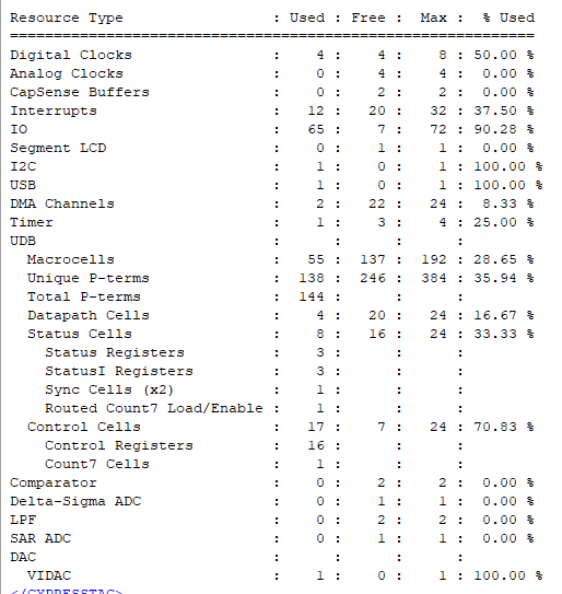
That did eat up some PSoC resources (mostly in the additional control registers), but there's still room. -
Interrupts on the PSoC
11/05/2019 at 15:43 • 0 commentsIn the last log we added support for interrupts on the PSoC. To summarize:
- There are (5) MCP23017 parts which connect to the PSoC
- MCP23017 parts communicate with the PSoC using I2C
- (1) Expansion MC23017 on the main board
- Port A and Port B have pull-ups enabled
- Port A and Port B inputs set to inverting
- Pulling input pin to ground causes a "1" to be read for the pin
- Connected to a JOYPAD on Port A
- Expansion MCP23017 ports are initialized as inputs
- Ports can be configured by Z80 writes (PIO control register format)
- (4) MCP23017 parts on the Front Panel
- Half of the pins on each MCP23017 are configured as inputs from pushbuttons and half as outputs for LEDs
- Ports can be read from the Z80
- The MCP23017 has two interrupt pins; one for A Port and one for B Port
- The (2) interrupt pins on each of the MCP23017 parts are wired together
- MCP23017 parts are set to Open Drain outputs on the Interrupt lines
- All [five] MCP23017 ports are Wire-OR tied together into one line - I2CINT*
- MCP23017 parts are set to interrupt on change of the input pins
- Any change (H>L or L>H) causes the interrupt lines to be asserted on the port's interrupt pin
- Every button press causes two interrupts one when the button is pressed, the other when the button is released
- Any change (H>L or L>H) causes the interrupt lines to be asserted on the port's interrupt pin
- The PSoC has to poll each MCP23017 to determine which MCP23017 part caused the interrupt
- The I2CINT* line is connected to pin 68 (P12[3]) on the PSoC
- An inverter inside the PSoC changes the active low signal into an active high signal
- The I2CINT* pin on the PSoC is connected to an interrupt function in the PSoC
- InterruptType is set to LEVEL
- PSOC Creator generates the API for the interrupt function which corresponds to I2CINT*
- API functions that can be called from "anywhere" include:
- I2CINT_ISR_Start( ) - Start up the function and enable interrupts
- I2CINT_ISR_Disable( ) - Disable interrupts from the I2CINT* pin
- I2CINT_ISR_Enable( ) - Enable interrupts from the I2CINT* pin
- API functions that can be called from "anywhere" include:
- Had to manually create a function to handle the Interrupt
- I2CIntISR( ) - Read the Interrupt capture registers into variables
- Reads the six INTCAP registers (two in the Expansion MCP23017 and the four halves from the switches of the Front Panel MCP23017 parts)
- I2CIntISR( ) - Read the Interrupt capture registers into variables
- The Z80 reset was tied to the MCP23017 reset line
- The MCP23017 couldn't t be initialized while it is held in reset
- The PSoC monitor couldn't be used to test the interrupt function
- Reworked the reset line to access interrupts from the PSoC Monitor
- Cut etch
- Add pull-up resistor since MCP23017 part doesn't have internal pull-up
After Reworking RESET* to the Expansion MCP23017
After doing the rework to the card, it now processes interrupts consistently. The ARM Core no longer gets heap errors, etc. However, the bounce of the switches is now a problem. If the code is set with a breakpoint at the end of the I2CINT_ISR routine it shows all key presses and releases are being received. If the ARM is running full speed it looks like some presses are being missed.
Possible Ways to Debounce and Have Interrupts
One way might be to disable interrupts when the interrupt is received and then use a timer to only enable interrupts again after some number of mSecs have gone by. That has the potential to be relatively simple. Would be the first time I've explicitly used timers, though.
- There are (5) MCP23017 parts which connect to the PSoC
3-Chip Z80 Design
Combining a Z80 retro design with a modern PSoC CPU.
 Most of the signals are directly from the Z80. Some of them are hard driven from the PSoC and would need to be changed to Open Drain outputs with pull-ups if there was an expansion card attached to this connector. I mostly want the connector to aid in debugging. Getting all those little chip clips on the Z80 pins and making them stay is just too hard. It's much easier to push the female pin from the Logic Analyzer onto a header.
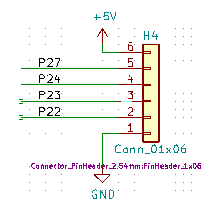
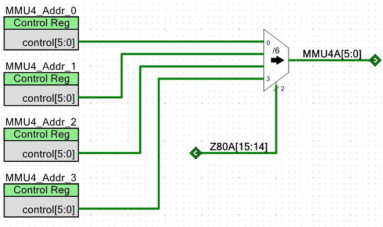
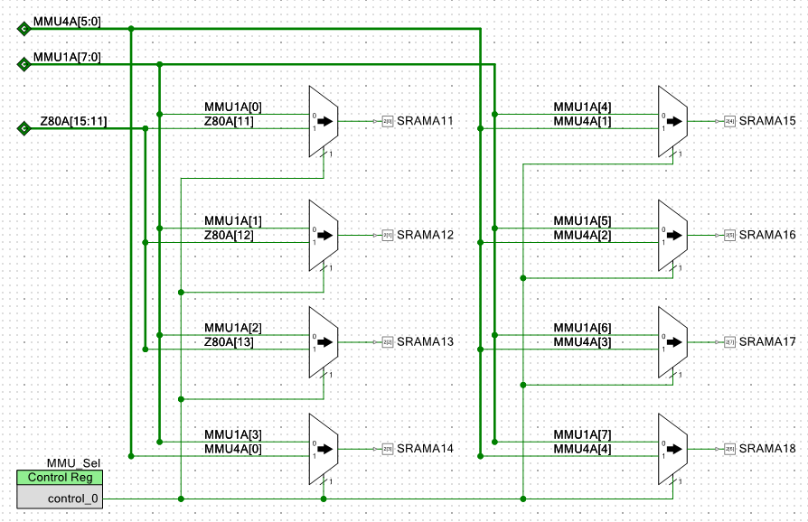 The current page that drives the MMU1 gets changed to go through the new level of multiplexer. My assumption is that PSOC Creator will reduce the logic automatically.
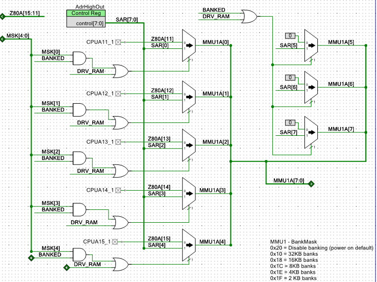 The HEX file from Multiboot Multicomp gets converted into a C array with srec_cat as previously done and added to the project. The Z80 IO handler gets updated to add handlers for the new Memory Mapper. The Harware_Config.h file gets updated to add the new Memory Map (USING_MEM_MAP_4) and top level design (MULTIBOOT_CPM). This is very similar to the 9-Chip CP/M design described in a previous blog.