land-boards.com
-
Added 4-Pin I/O Header
09/22/2019 at 00:55 • 0 commentsCould use for Serial port with handshake in place of USB host.
-
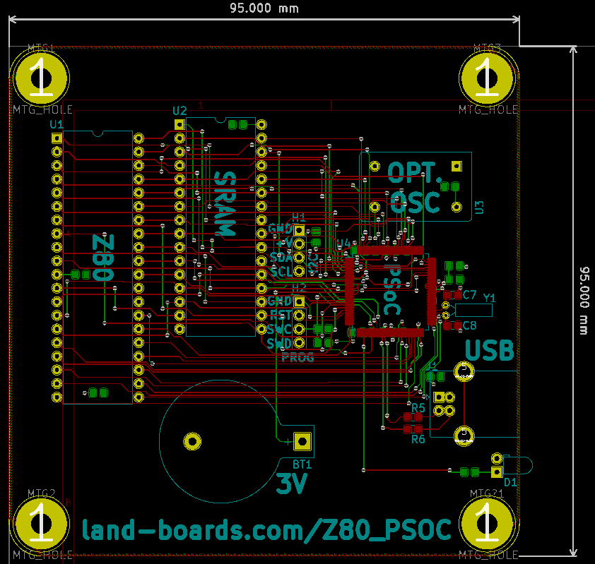
Routed PCB
09/22/2019 at 00:44 • 0 commentsHere's the routed PCB.
![]()
Features:
- PSoC 5LP
- USB-B connector
- LED controlled by the PSoC
- Z80 CPU
- 512KB SRAM
- Real time clock+battery.
- The oscillator is optional
- I2C connector
- Download cable header
- ODAS form factor (95x95mm)
- Mounting holes
-
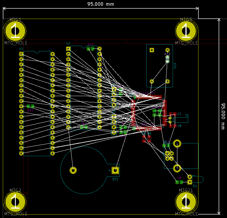
Notional Parts Placement
09/21/2019 at 18:41 • 0 commentsHere's my cut at the parts placement. This should fit onto a 2 sided card. I put the passives on the back of the card (mostly). Parts easily fit into my ODAS form factor and being less than 100x100mm are inexpensive to have fabricated.
![]()
-
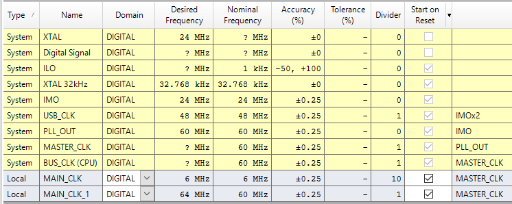
Z80 Timing Generation
09/21/2019 at 14:37 • 0 commentsThe PSoC includes a somewhat complicated timing circuit with internal PLLs. There's a GUI for configuring the Internal clocking. It can also be driven with an external oscillator for increased accuracy for generation of serial data. This would only be necessary if a serial port was used. An external crystal is not required for USB serial since the PSoC generates this timing internally.
A 32.768 KHz watch crystal and button battery can be connected to the PSoC to provide Real Time Clock functionality. This is enabled by selecting the XTAL 32KHz check box.
The Internal Master Oscillator (IMO) is an accurate clock with 0.25% accuracy when run at 24 MHz. This accuracy is needed for the USB bus which multiplies it by 2 to 48 MHz. This is the source of the other clocks.
![]()
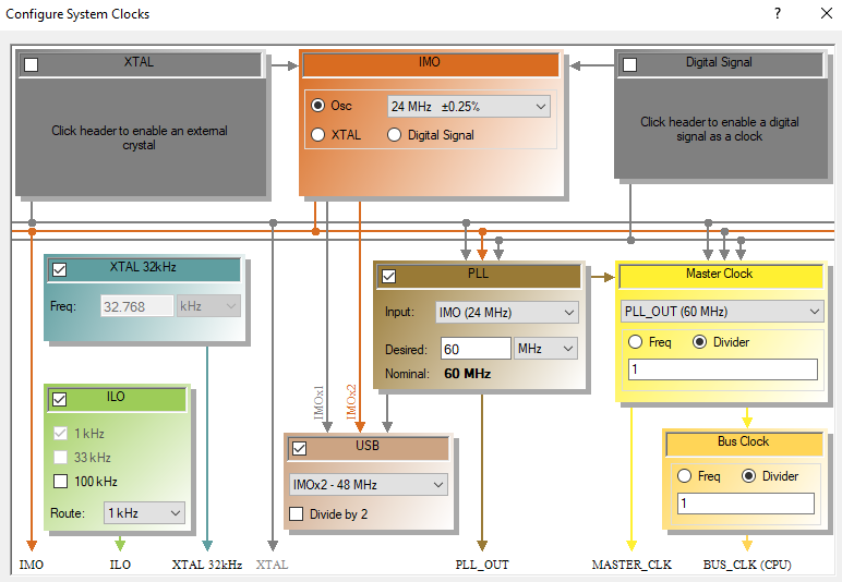
The clocks look like this.
![]()
The PSoC can run faster, but the Z80 CPU clock is 6.0 MHz so running the PSoC at 60 MHz is a convenient multiplier. It could also be run at 63 MHz and still provide a 6 MHz clock.
An accurate baud rate clock is not needed if the USB interface is used.
-
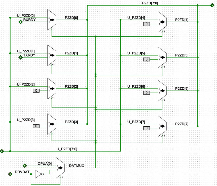
Z80 I/O Registers
09/21/2019 at 14:05 • 0 commentsThe Z80 needs to be able to read the (PSOC to Z80) data register and status register. This requires a read multiplexer. Here's the path for the Z80 Read Data lines:
![]()
The bits of the status register are:
D0 = Receive Data Ready
D1 = Transmit Data Ready
D2-D7 = 0
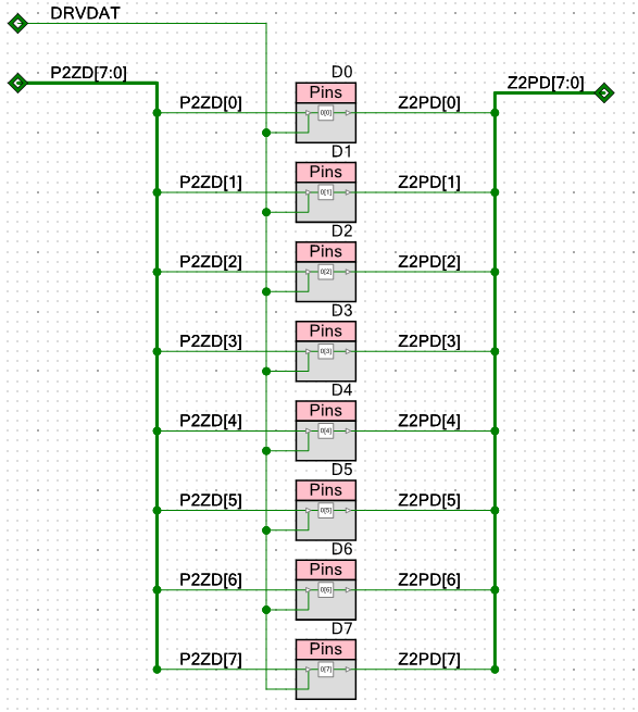
The data bus pins to/from the Z80 are bidirectional. I've chosen to name the pins similar to SPI bus notation. P2Z is PSoC to Z80 and Z2P is Z80 to PSoC. Hopefully this will minimize confusion.
![]()
-
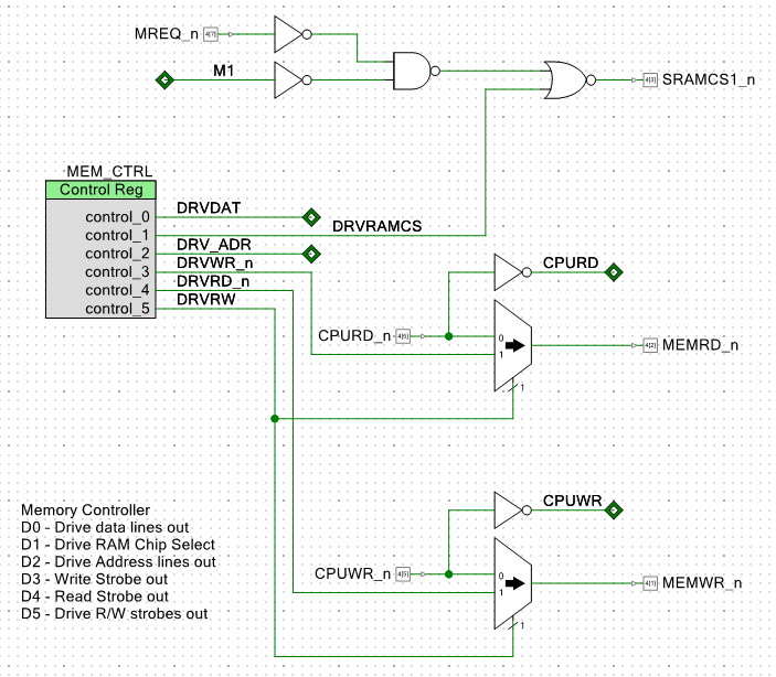
Memory Mapping/Banking
09/21/2019 at 13:18 • 0 commentsThere is only one device in the memory space, a 512KB SRAM. The Z80 only supports 16-bits of address. This function does bank switching and mapping.
There are software builds for the Z80 which have ROM and RAM. The RAM is typically copied to the RAM and then the program is run out of RAM. CP/M builds use this method. Part of this was that the EPROMs of the day were relatively slow compared to RAM. Today, RAM is very fast. Maybe too fast.
Switching between the banks varies by the hardware implementation and software needs. The PSoC can go a low way towards this functionality by performing banking control. This circuit is a first cut at that.
Chip Selects and Read/Write Strobes
![]()
Banking
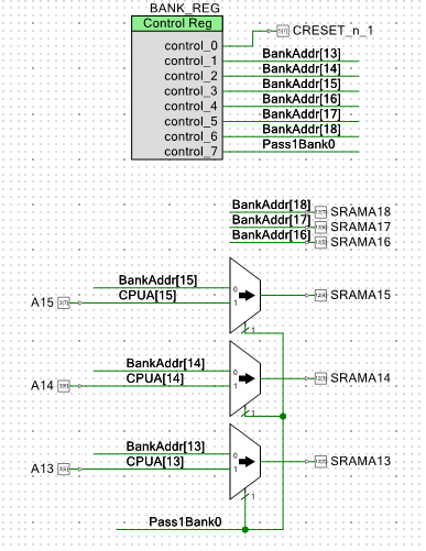
Banking consists of re-mapping some of the upper bits of the Z80 address bus into more address bits of the SRAM. This could be done purely in hardware with a small mapping function (like a RAM) or with the help of the PSoC. This means the PSoC writes to the BANK_REG with the upper SRAM address lines. For this implementation I've chosen to bank switch address lists 13..15. This provides for 8 banks. These three bits map to SRAM 13..18 address lines.
![]()
There will probably need to be some more registers for mapping but this logic provides a "direct" path where the CPU addresses go directly through (all 64KB are directly mapped) and the ability to swap in upper bits from the bank register values.
The I/O select logic (previous page) indicates to the PSoC that a bank select operation needs to be done.
-
Peripheral Chip Emulation
09/21/2019 at 13:06 • 0 commentsThinking through the PSoC design and how to implement peripherals. Want:
- Mailbox with status register (read/write ready)
- I/O Address Latch
- 8-bit Data Read/Write register
Z80 I/O Address Latch in PSoC
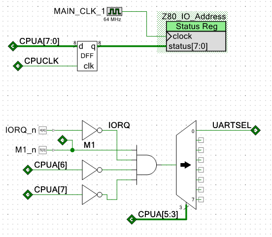
Latches the 8-bits of address from the Z80. This address can be read by the PSoC via the Z80_IO_Address Status Register.
I/O Chip Selects can be hard decoded.
![]()
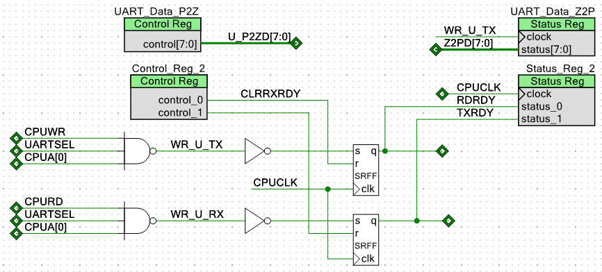
I/O Mailbox
The I/O mailbox circuit is implemented with data and control/status register as follows:
![]()
The PSoC writes to the UART_Data_P2Z register which can be read from the Z80. RS Flip Flops are set when the UART_Data_P2Z is written from the Z80 or UART_Data_Z2P is read by the Z80. Bits from the Control_Reg_2 is used to clear the RS Flip Flops. Status_Reg_2 is used to read the output of the RS Flip Flops by (or can cause interrupts to) the PSoC.
3-Chip Z80 Design
Combining a Z80 retro design with a modern PSoC CPU.