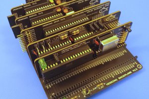
 EtchedPixels
The board implements an expanded mode 6303 set up and generates Z80 like signals from the CPU in order to drive the bus. A 74HC00 does the needed conversions to generate the \RD and \WR lines whilst a 74HC688 is used to generate \IORQ and \MREQ by mapping MMIO $FExx to the I/O space.
One 74HC573 demultiplexes the lower address and data lines. The second one is present as the recommended workaround for the fact that you can get big transients when the lower address lines switch to data, and buffers the upper address lines which if there are power problems or a lot of capacitance can otherwise wobble when driving a high capacitance load - like a backplane.
The spare port when running multiplexed is brought out on the top of the board for purposes yet undefined (it's an 8bit GPIO port so quite flexible). Port 2 is brought out for the TTL serial and the other port 2 pins are just strapped to get the desired boot mode.
Clocking is a bit different to the other boards I've made. The 6303 card expects a standard RC2014 clock/reset card because it runs at CLK/4 and generates that
There is a jumper to put the actual E clock on pin 39 (a user pin) but it's actually not very useful without RW. If I do a rework of the board I'll move it to pin 38 with RW on pin 39 and 680x peripherals would prefer to have both, and 6502 already uses pin 39 for RW.


 Colin M
 SHAOS
SHAOS
I have a 6803 board that has a 6845 controller and colour video graphics routines. Feel free to hack the code for your own project:
https://hackaday.io/project/177606-stebus-68456803-video-board