Alexis
-
Videos!
06/25/2021 at 00:42 • 0 commentsI don't know why, this site removed the post with the videos. Here they are!:
-
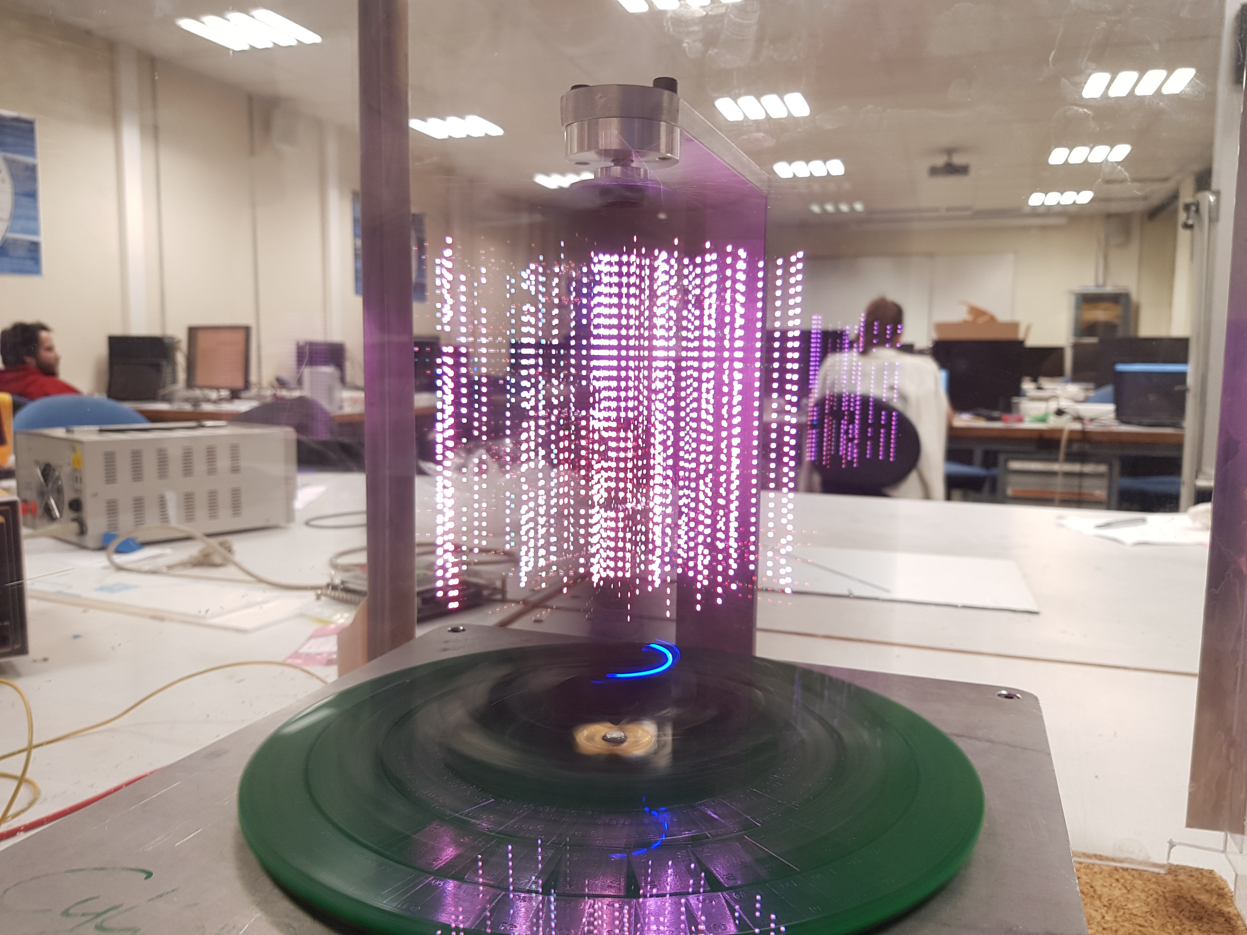
Final result!
06/13/2021 at 18:20 • 0 commentsEverything is working ! Now on for the videos :-)Teacher (Alexis)'s word to the team : congrats for this amazing work !
All details and logs can be found here: https://rose.telecom-paristech.fr/2019/tag/cyl3d
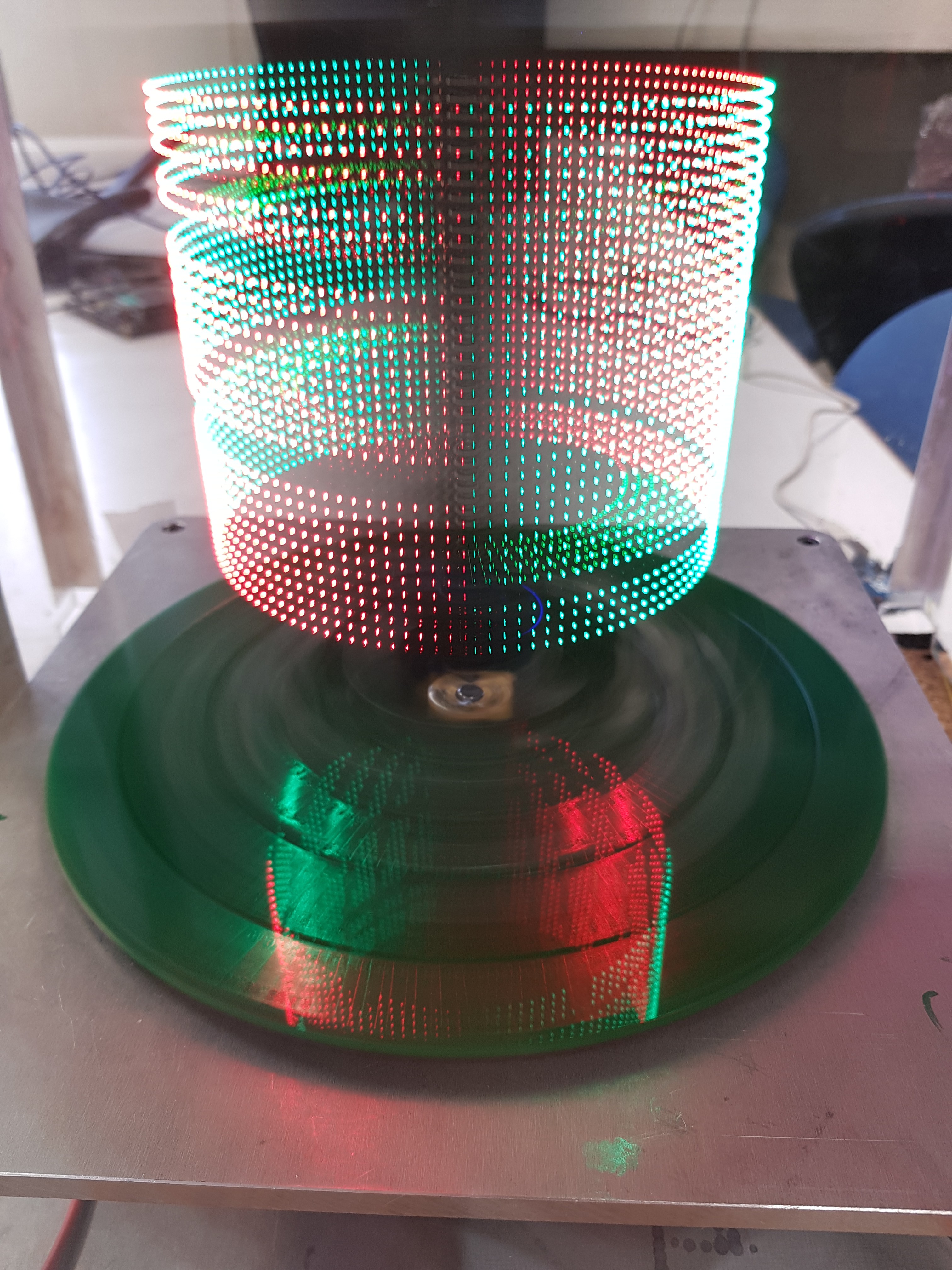
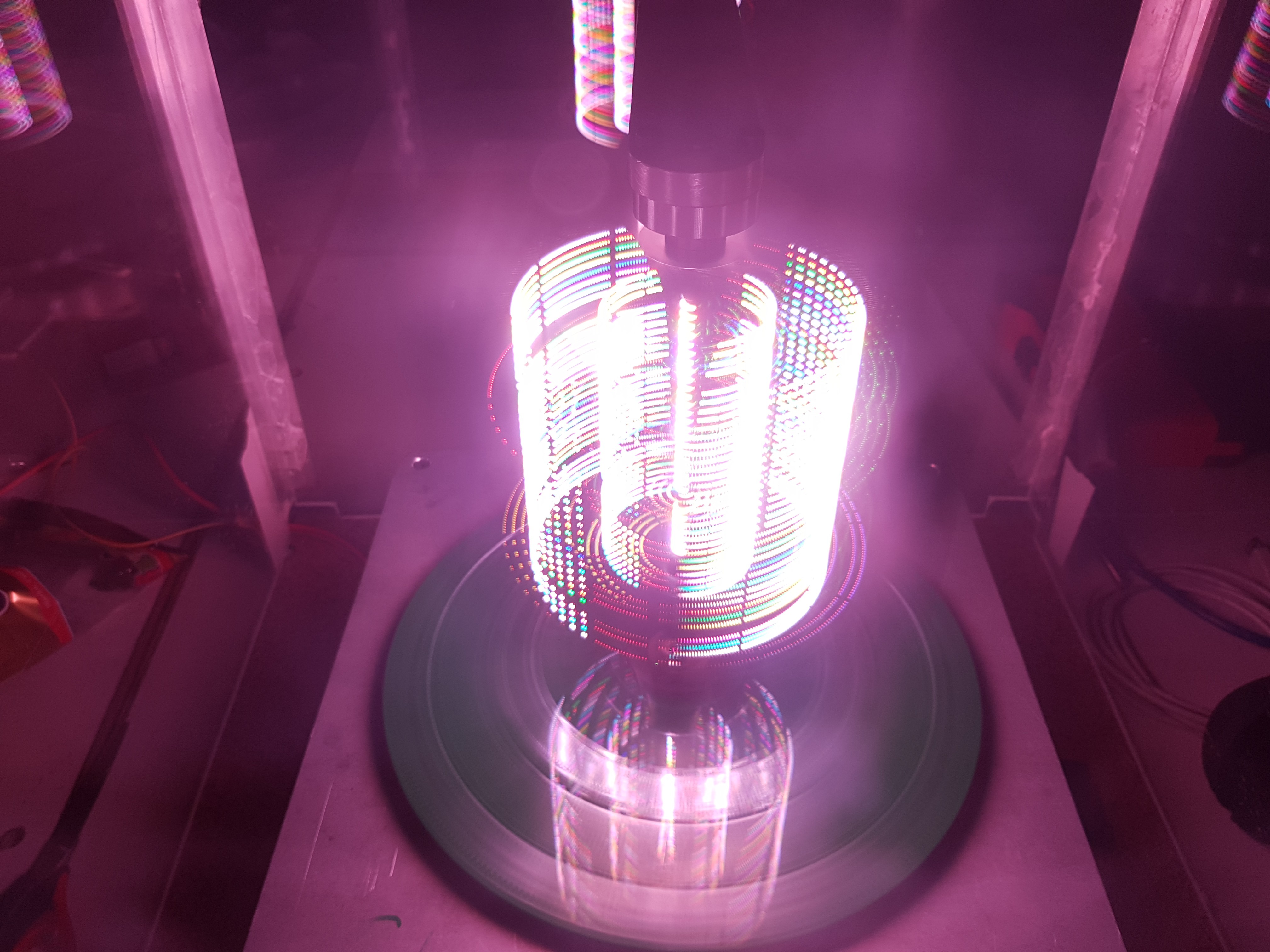
First tests:
![]()
![]()
![]()
And it's finally working!
![]()
-
FPGA debugging
06/13/2021 at 18:17 • 0 commentsBy Ambroise:
We are using the PIO core IP from Intel to implement debug registers accessible from the HPS to communicate easily with the FPGA. After testing that we could read and write such a register, I implemented a shell accessible in a Linux terminal inspired from ChibiOS.
I used those IPs to act as bypass registers in our FPGA modules. The implementation is still ongoing, but I currently have a shell command to test the correct soldering of the LEDs (by lighting all of them in a dim white).
The next step will be to complete all of our FPGA modules as well as their basic bypass register and test-benches (should be done by Monday).
-
HPS FPGA
06/13/2021 at 18:16 • 0 commentsBy BP:
I’ve been working on the HPS/FPGA communication, and how we will handle buffering.
Architecture
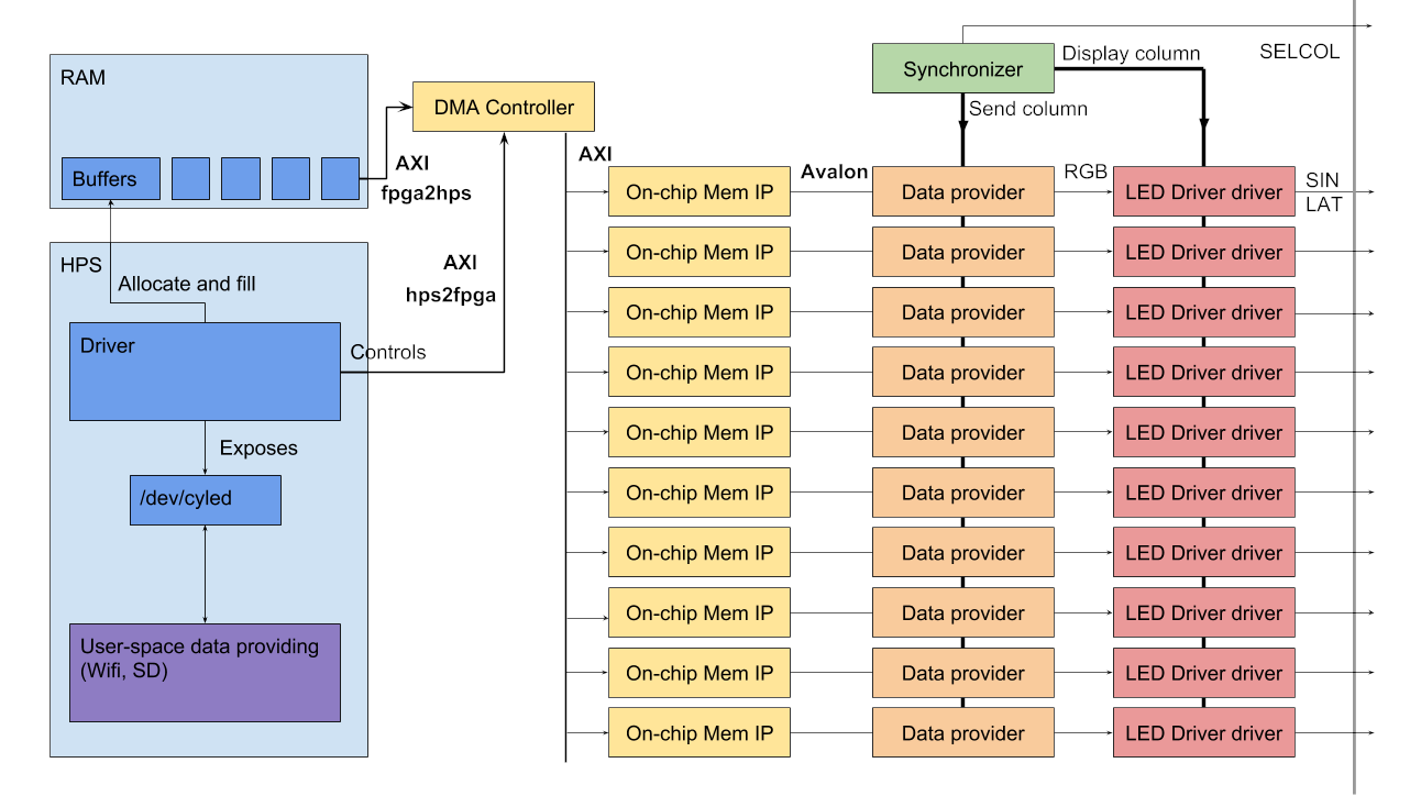
I came up with this completed version of the architecture:
![]()
FPGA buffers will be fed by a DMA Controller. The DMAC will read data from RAM using the fpga2hps bus, and write to an AXI bus connected to all FPGA buffers.
On the HPS side, we will have a kernel module controlling the DMAC through the hps2fpga bus. It will be responsible of DMA transfer sequencing (between all buffers), and also the transfer timing.
The DMA source will be a pool of contiguous RAM buffers allocated by the driver.
Finally, the driver will expose a Linux char device. Through this device, a user-space app will be able to feed the buffers with data from various source (an SD card, a Wifi streaming).
Buffering
If you think about it, each half frame-slice will need to be printed twice, for it to be seen from all points of view. Thus, the drawing flow looks like this (where each line is a half turn, and the two numbers represents the frame being drawn by each half of the panel) :
- F(n, right) ; F(n+1, left)
- F(n+1, left) ; F(n+1, right)
- F(n+1, right); F(n+1, left)
- F(n+1, left) ; F(n+2, right)
- …
We can see that the first half always get data from the second half at previous round. Thus, if we swap buffers smartly across drivers, we can use half-a-turn buffers. This results in 3 buffers for 2 drivers storing (F(n), right), F(n+1, left), F(n+1, right)), where at each time, one buffer is useless and can be fed by the DMAC with the next correct half.
To start with simpler code, we will approximate to 1 buffer per driver (+33% data stored), with a full turn capacity. We will optimize only if needed, that is, if the throughput of the HPS -> FPGA is not sufficient to transfer that much data.
In RAM, we will have a double buffer. One where we write data for the next turn, and one with data that should be used during this turn.
-
PCB done, FPGA started
06/13/2021 at 18:13 • 0 commentsBy BP:
Routing
It’s been a long time since the last post. I’ve been busy finished the routing of our vertical PCB. We use 4 layers, layer 2 being a GND plane.
Here is the routing layer by layer, with explanations:
![]()
Layer 1 (top) ![]()
Layer 3 ![]()
Layer 4 (bottom) FPGA architecture
Since we’re done (modulo reviewing) with the PCB, we started thinking about the FPGA architecture.
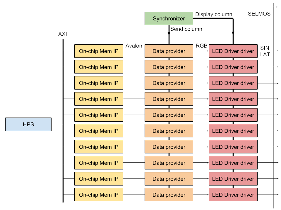
We came up with an architecture based on 4 modules.
- We will use the Altera On-chip Memory IP as our per-driver buffers. It is practical since it has an AXI-compatible interface that we can use to easily connect to the HPS.
- A synchronizer module will be in charge of time-keeping in order to load and display data at the right time. It will also select which column to display.
- The data provider will load data from the memory and pass them to the LED-driver driver.
- Finally, the LED-driver driver is in charge of creating the SIN/LAT signals. It will both send data to the driver (as requested per the data provider), and display those data (as requested per the synchronizer)
![]()
-
Rethinking the motor
06/13/2021 at 18:10 • 0 commentsBy Guillaume:
We had a long discussion with a student from SpiROSE (last year’s project with a rotative LED panel). He told us the problem they faced with the motor and ESC (Electronic Speed Controller). They could not get a constant speed output from the motor because the ESC was overheating, causing a shutdown and a boot up. It was caused by the motor asking too much current. The motor was one the had on hand and not perfectly fitted to their use. It was rated at 2100 RPM per Volt. While turning at 1500 RPM the ESC pulled 5A on 12V from the power supply, the same 60W would go to the motor, but to rotate at 1500 RPM it only needed 0.7V so the output current from the ESC was closing in on the max output, which caused overheating.
So I am looking for a motor with a lower RPM per Volts constant. I reckon a motor at around 500 RPM/V would be suitable for our project. For now I have have settled on Turnigy Aerodrive SK3 – 4250-500kv Brushless Outrunner Motor from HobbyKing.
Another problem was to convey the power through the axis. They had to scrub the anodising paint from the top of the motor to make a connexion to a ball bearing which was connected to the motor shaft. I would like if possible to stay away from passing to much power through the ball bearing as it can cause sparks and damage the balls. To replace this connection I am looking toward brush slip rings.
-
Size constraints
06/13/2021 at 18:09 • 0 commentsBy Ambroise:
As we are proceeding with the schematics and the PCB placing, we are realizing that we will need more than a single PCB to make everything fit. We will then design an horizontal PCB, very much like SpiRose, though ours will be rectangular for budgetary reasons and it will only host our voltage regulators. The interface between the horizontal and vertical PCBs will be three big pads: GND, 3.3V and 5V. Hence, no signal integrity concerns (at least not at this interface). I placed our 12 to 5V converter on Xpedition Layout while conforming to the PCB layout guide of the module.
![]()
LMZ12010 Furthermore, it appears that the PCB size of 190 by 190mm that we initially chose will be problematic for us to solder the LED automatically: the problem being the width of the PCB. I was going through the process of routing the LED drivers so that we could be stacking five of them on each side of the panel (according to our previous PCB layout idea), but that will have to be abandoned in order to make our PCB thinner. We will put 4 driver on each side and 2 above.
-
Finalizing the schematics of our ULPI transceiver
06/13/2021 at 18:08 • 0 commentsBy Paul:
Last friday we had a class about signal integrity. As we learnt about all the problems we could have, I finally understood the use of all the bypass capacitors and some of the other esoteric symbols or annotation that are no longer a mystery (such as 0-ohm resistors or DNI annotations)
Thus, I had to update the schematic of the ULPI/USB subsystem of our project. You can see it below. Here are some important changes :
- Disconnected the oscillator ENA pin : according to the datasheet, having the pin on high impedance does enable the oscillator.
- Added USB power distribution switch, the TPS2051C that is needed not to break our USB device. It limits the current of our usb device to 500mA.
- Added bypass capacitor to oscillator and power switch.
- Updated power supply capacitors
- Added 10K resistor for VBUS, connected to a 10uF capacitor that should be enough for our system. The USB 2.0 specification recommends a 120uF capacitor for hosts but we do not intend to hot-plug our USB device or have a cable between our device and our system.
- Added names to everything.
- Connected the RESETBn pin to our nRST.
![]()
ULPI/USB Subsystem Schematic As such, our ULPI/USB system should work. However, I have a doubt about whether or not I should add a resistor on the wire between the oscillator’s CLK and the USB3320C REFCLK. Our development kit has a resistor on its schematic, but the oscillator’s datasheet does not mention to put a resistor on the CLK output. If anybody has an idea about it, I’d be happy to hear it.
-
Booting the FPGA & Schematization of the USB3320
06/13/2021 at 18:08 • 0 commentsBy Paul:
For the past days, I have been working on the schematics of our ULPI transceiver, the USB3320 and when my colleagues were working on other parts of the schematics, I had to focus on other stuff such as making our SOM work and improving our system architecture.
Making our Cyclone V SOM work was a breath of air compared to the schematic part. Following the Quick Start Guide of our development kit, I had to make sure the jumpers were setup correctly (and they were – not sure if it was the factory default or if Alexis did his magic before giving us the devkit) and configure the UART0 interface. Once everything was set and connected on /dev/ttyUSB0, I simply plugged in the devkit and it booted correctly.
You can see the booting log on this pastebin post.
As we would like to be able to use Wi-Fi USB dongles, we are currently adding host USB 2.0 support. Unfortunately, we must use the ULPI interface to communicate with our USB devices. Thus, we have to use a ULPI-USB transceiver.
ULPI works with a 60MHz clock and I am unsure for now if our FPGA can generate such an accurate reference. However, the USB3320 can work with a external oscillator and it has its own PLLs to generate a 60MHz clock from a 12MHz reference clock.
Below is a work in progress of the schematic of the USB3320 in our system. It also includes a Linear Voltage Regulator as the transceiver also needs a 1.8V DC supply.
What is definitely missing are the appropiate capacitors and resistors that I have not added everywhere yet.
![]()
USB3320 Schematic (WIP) -
Decoupling of the SoM
06/13/2021 at 18:06 • 0 commentsAltera made a spreadsheet named “Power Delivery Network” designed to determine an optimum number, type and value of decoupling capacitors to achieve the target impedance. I select the VRM type (Switcher), the supply voltage (3.3V), maximum current (2.58A), transient current (I typed 30%, but it seems extremely complicated to obtain a value without having the programming of the FPGA already done) and ripple tolerance (5% given the specifications of the FPGA and knowing that we don’t have transceivers for PCIe, which is the only bank requiring at most 3% ripple). For the spreading inductance, BGA Via inductance and plane capacitance profile I left the default values because I don’t know how to estimate that.
Auto decoupling
The tool looks up the capacitors it has in its database and tries to find the optimal combination for our target. With the preceding values it outputs 2x 0.01µF, 2x 0.047µF, 1x 1µF and 1x 10µF capacitors, with their respective ESR, ESL and mounting inductance (Lmnt).
![]()
Auto decoupling Development board decoupling
![]()
Development board decoupling: capacitors If I take the configuration of the development board of our SoM, they are using 4x 10µF and 9x 100nF capacitors. If I use the capacitors pre-configured in the Altera tool, it shows that the resulting impedance is higher than the one I got with my inputs, but given that the development board has to be designed for any configuration of the FPGA, their decoupling capacitors are certainly adapted to more extreme power draws than what we will be experiencing. So, I think it would be a good idea to keep what Aries did with their development board.
![]()
Development board decoupling: impedance