schwarzrmsu
-
Updating DAC Reference
02/23/2020 at 19:02 • 0 commentsIn my last post I explained how transitioning from the external 3.3V reference to the internal 4.096V reference will help increase the accuracy of the DAC's output voltage. In this post we are actually going to update the HW and SW in order to transition from the external reference to the internal reference.
In order to use the DAC's internal 4.096V reference, we need to power the DAC from a voltage source that is higher in voltage. Unfortunately the only two voltage rails we currently have available are 12V & 3.3V. 12V is too high for the DAC, and 3.3V is too low to use the internal reference. Therefore we need to add a 5V rail which will be used to power the DAC. 5V is perfect because its higher than 4.096V, and lower than the maximum allowable voltage for the DAC.
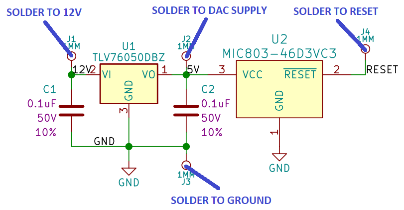
This type of update requires a mod board, therefore I designed one. Below is a screen shot of the schematic:
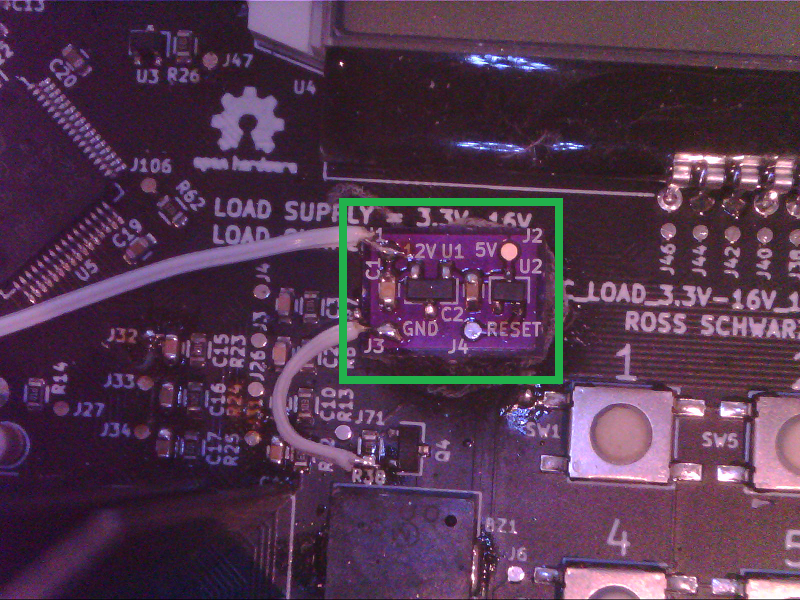
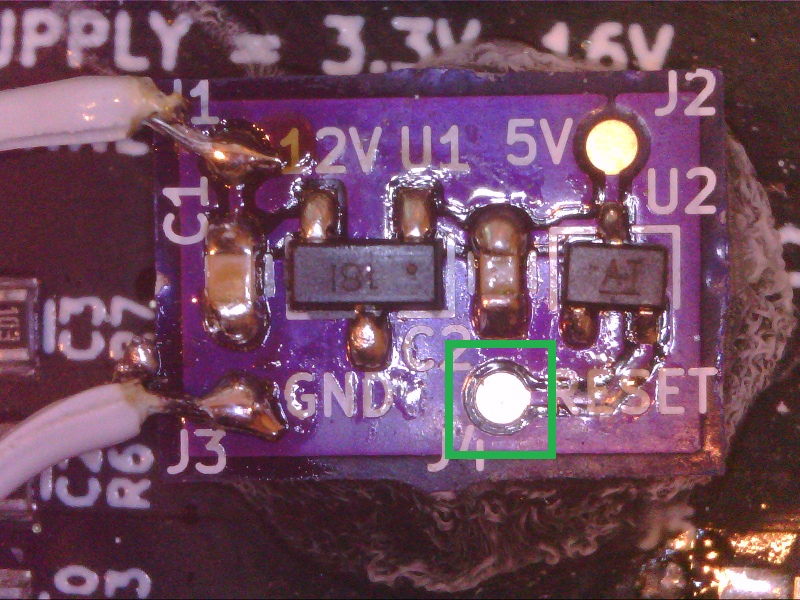
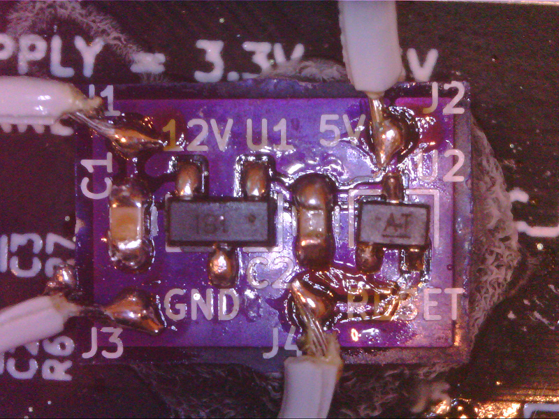
As you can see I am using a simple TLV76050DBZ 5V linear regulator, and I also added in a MIC803-46D3VC3 voltage monitor. The voltage monitor will pull the reset line low when it detects the 5V regulator has dropped out.
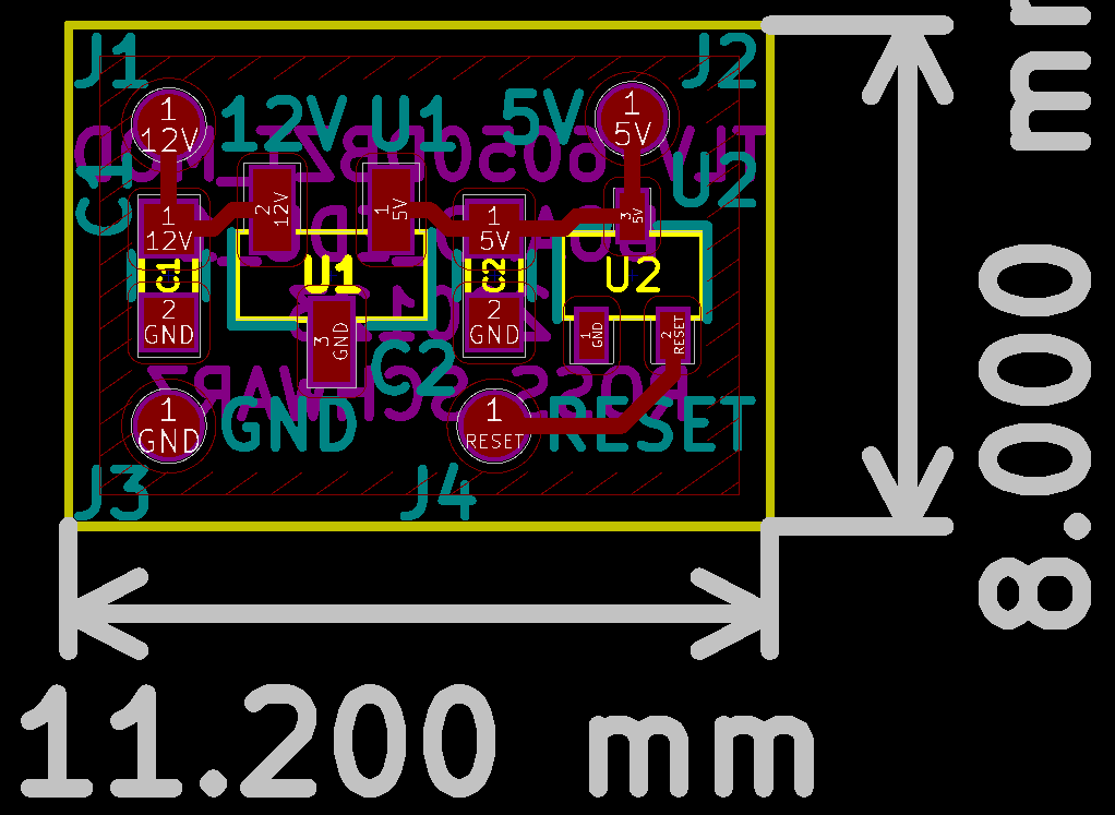
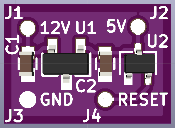
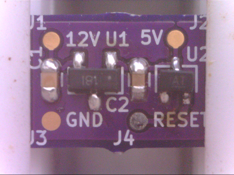
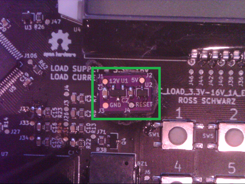
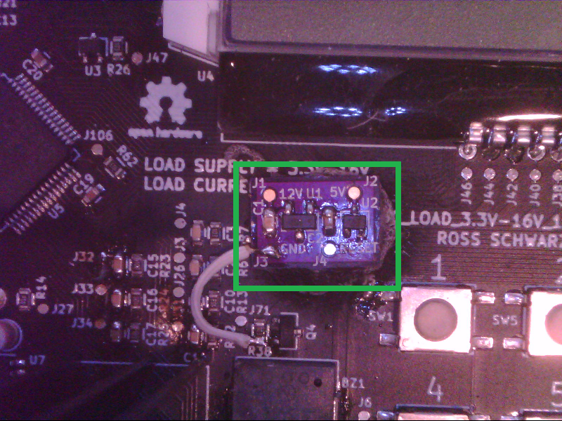
I designed a very small PCB that can be glued to the existing PCBA, and then wired in by soldering wires between mod board and main PCBA. Below are screen shots of the mod board:
Board Layout:
3D Rendering:
Hand Soldered PCBA:
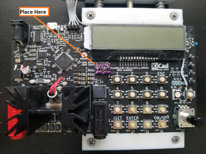
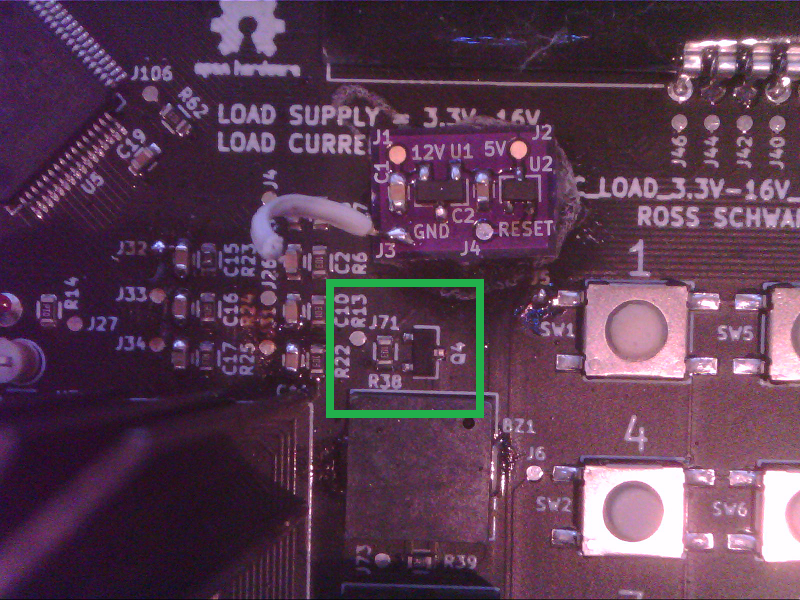
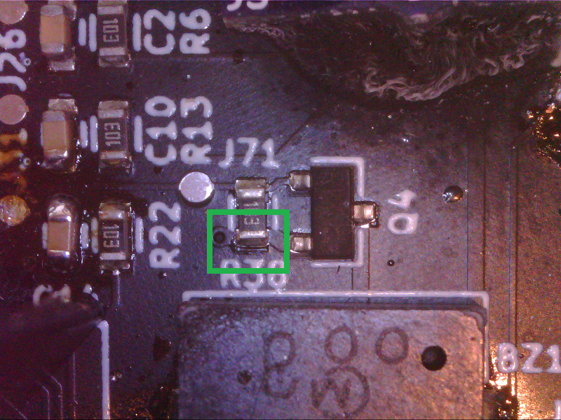
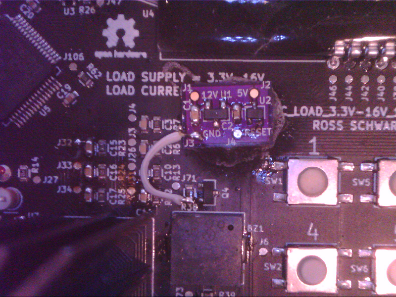
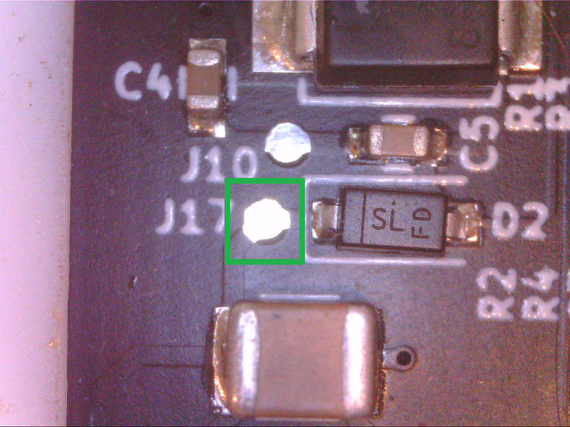
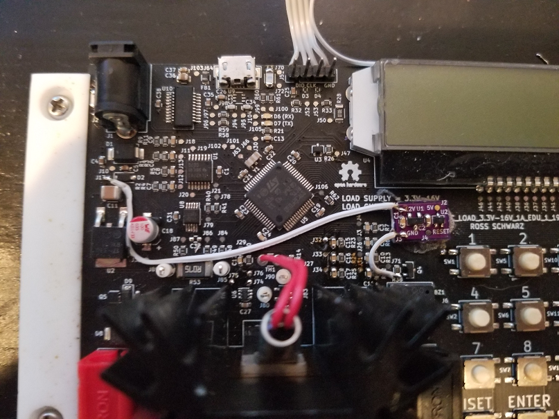
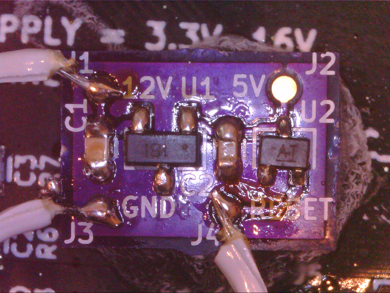
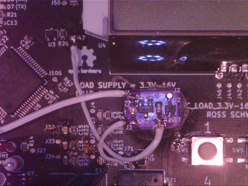
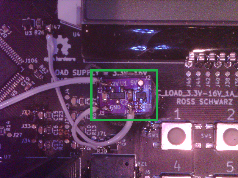
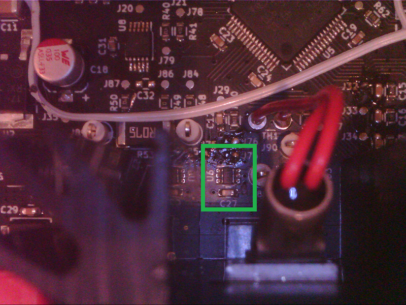
Now we will take this mod board and glue it to the PCBA in an area that does not have any components, and is close to the nets that we need to solder to. Unfortunately I did not have an amazing place, but I settled on this location:
Now we need to wire the mod board to the PCBA. We will need to connect Ground, 12V, Reset and 5V. Below is a walk through on how to do so:
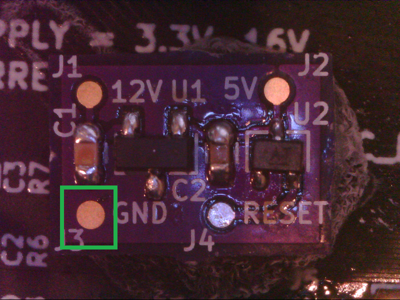
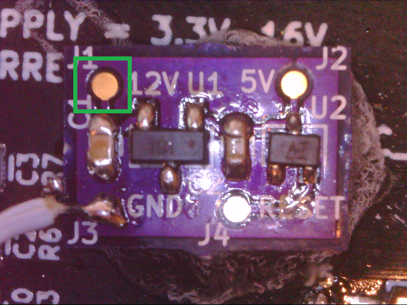
First we are going to route the wire for ground. Locate the mod board PCBA:
Locate the ground connection on the mod board PCBA:
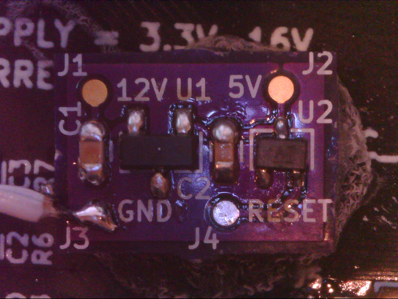
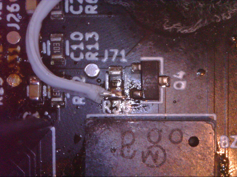
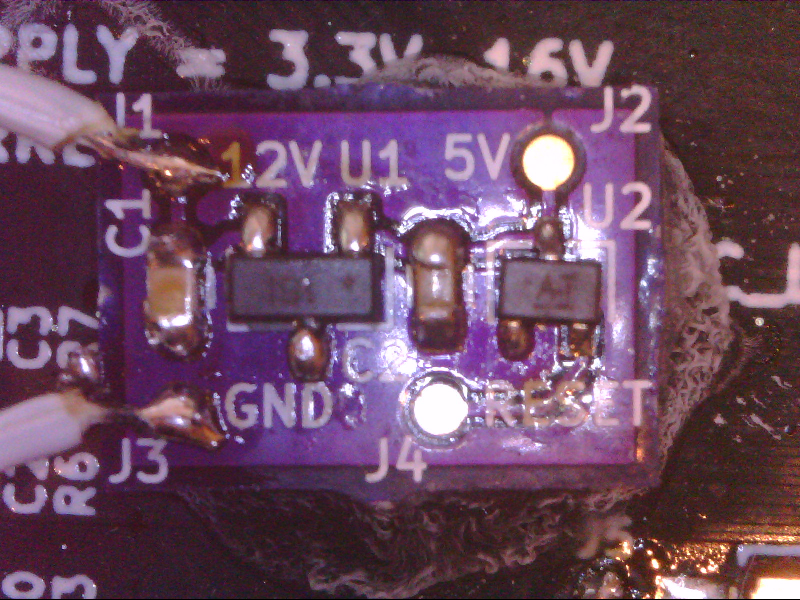
Solder a wire to the ground connection:
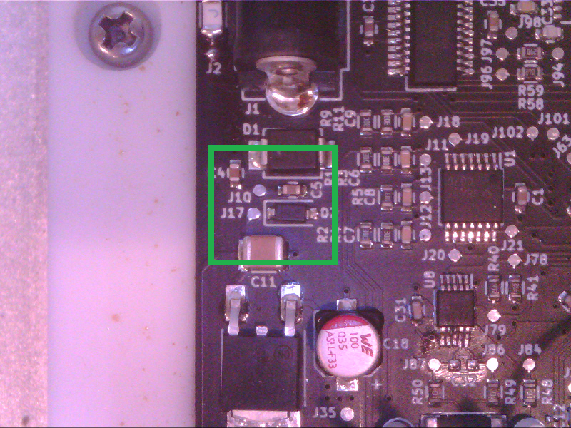
Locate area of main PCBA with ground connection:
Locate ground connection:
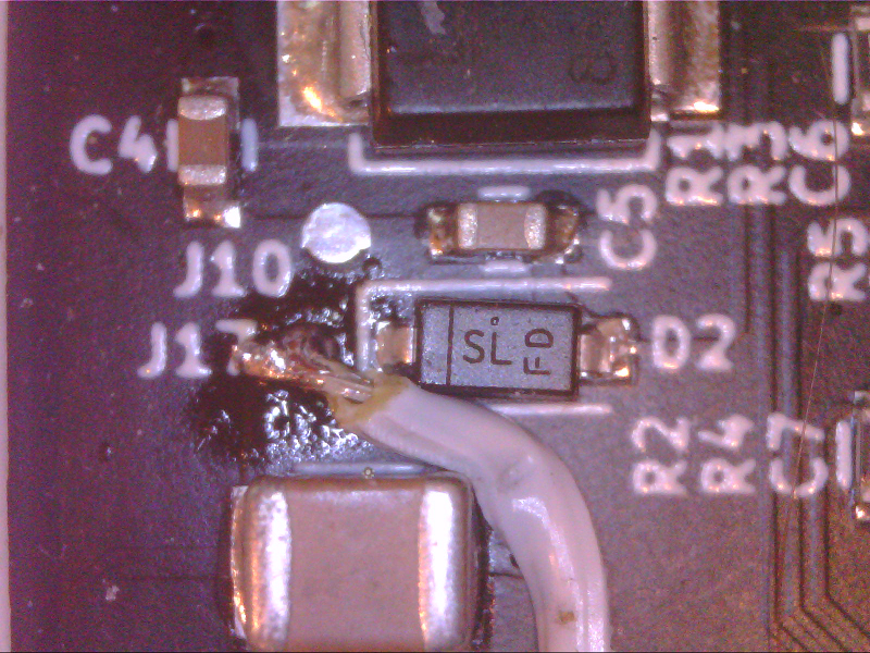
Solder other end of wire to ground connection:
Look over ground connection wiring:
Next we are going to route the wire for 12V. We can start by locating the mod board PCBA:
Locate 12V connection on mod board PCBA:
Solder a wire to the 12V connection:
Locate area of main PCBA with 12V connection:
Locate 12V connection:
Solder other end of wire to 12V connection:
Look over 12V connection wiring:
Next we are going to route the wire for Reset. We can start by locating the mod board PCBA:
Locate reset connection on mod board PCBA:
Solder a wire to the reset connection:
Locate area of main PCBA with reset connection:
Locate reset connection:
Solder other end of wire to reset connection:
Look over reset connection wiring:
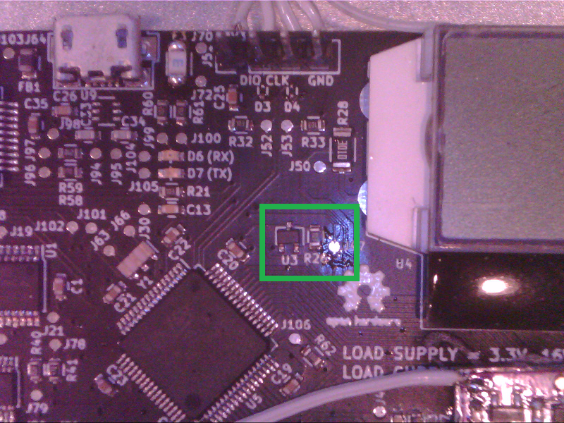
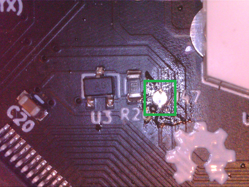
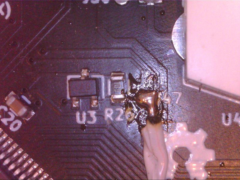
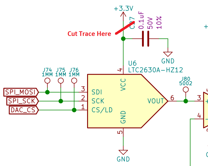
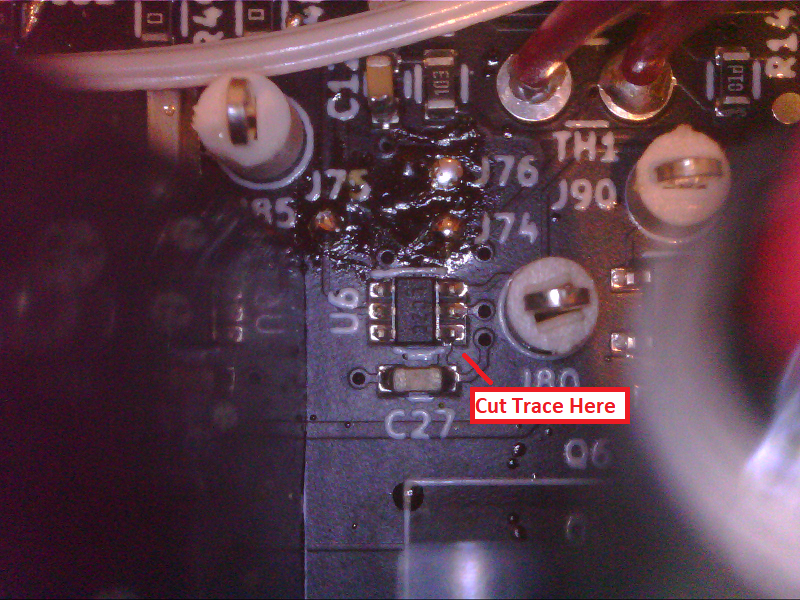
Lastly we are going to route the wire for 5V. First we need to cut the trace that was originally connecting 3.3V to the DAC:
Locate the area of main PCBA with this trace:
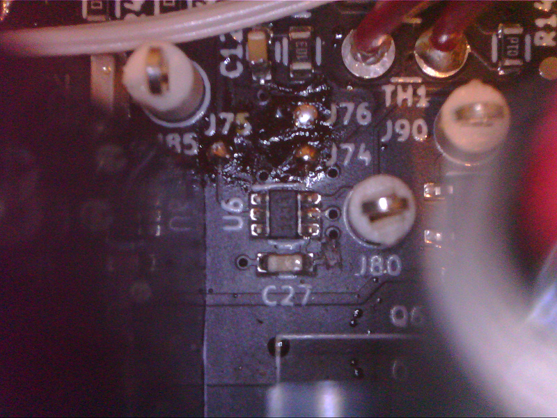
Cut the trace:
Now that the trace is cut, we can route the wire for 5V. We can start by locating the mod board PCBA:
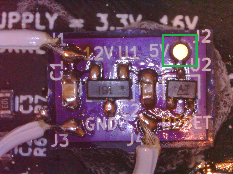
Locate 5V connection on mod board PCBA:
Solder a wire to the 5V connection:
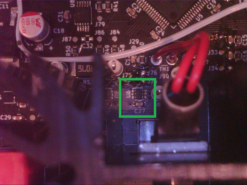
Locate area of main PCBA with 5V connection:
Locate & Solder 5V connection:
Look and review all of the wiring. It is suggested to ring out each connection to check soldering:
Lastly we need to update the SW to use this internal reference. Below is the SW in order to generate 1V at the DAC output:
uint8_t DAC_writeToAndUpdateDACRegisterCmdCode = 0b0011;
uint8_t DAC_selectInternalReferenceCmdCode = 0b0110;

uint16_t DAC_vSetData_u16 = 999;
uint8_t DAC_dataUpperByte_u8 = 0;
uint8_t DAC_dataMiddleByte_u8 = 0;
uint16_t DAC_dataMiddleByte_u16 = 0;
uint8_t DAC_dataLowerByte_u8 = 0;

DAC_dataUpperByte_u8 = DAC_selectInternalReferenceCmdCode << 4;
HAL_GPIO_WritePin(DAC_CS_DO_PORT, DAC_CS_DO_PIN, RESET);
HAL_SPI_Transmit(&hspi1, &DAC_dataUpperByte_u8, 1, 10);
HAL_SPI_Transmit(&hspi1, &DAC_dataMiddleByte_u8, 1, 10);
HAL_SPI_Transmit(&hspi1, &DAC_dataLowerByte_u8, 1, 10);
HAL_GPIO_WritePin(DAC_CS_DO_PORT, DAC_CS_DO_PIN, SET);

DAC_dataUpperByte_u8 = DAC_writeToAndUpdateDACRegisterCmdCode << 4;
DAC_dataMiddleByte_u16 = DAC_vSetData_u16 >> 4;
DAC_dataMiddleByte_u8 = DAC_dataMiddleByte_u16;
DAC_dataLowerByte_u8 = DAC_vSetData_u16 & 0b1111;
DAC_dataLowerByte_u8 = DAC_dataLowerByte_u8 << 4;

HAL_GPIO_WritePin(DAC_CS_DO_PORT, DAC_CS_DO_PIN, RESET);
HAL_SPI_Transmit(&hspi1, &DAC_dataUpperByte_u8, 1, 10);
HAL_SPI_Transmit(&hspi1, &DAC_dataMiddleByte_u8, 1, 10);
HAL_SPI_Transmit(&hspi1, &DAC_dataLowerByte_u8, 1, 10);
HAL_GPIO_WritePin(DAC_CS_DO_PORT, DAC_CS_DO_PIN, SET);
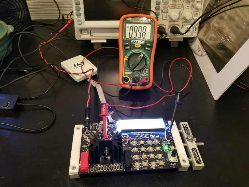
Once the HW and SW updates were complete, I probed the output of the DAC to confirm 1V is present:
I hope you enjoyed my post. Thank you for reading. Please feel free to leave a comment below.
Thanks again.
-
DAC Voltage Reference Worst Case Circuit Analysis
02/16/2020 at 14:24 • 0 commentsI noticed when writing my last post Digital To Analog Converter Control Using SPI that the voltage reference that I planned on using was not going to be possible. I planned on using the internal 4.096V reference of the LTC2630, but I mistakenly only powered my DAC from a 3.3V voltage regulator. Therefor in the short term I set my reference to be the supply voltage of 3.3V. In this post I am going to explain why I want to use the 4.096V reference.
The reason the voltage reference for the DAC is so important, is because the voltage reference can be a large contributor to the accuracy of the DAC's output. DAC's simply take your reference voltage, and split it up into a number of steps, depending on the number of bits. The LTC2630 is a 12 Bit DAC, therefore it splits the reference into 4095 steps.
The voltage reference accuracy is important because the SW assumes the reference is perfect, but in reality the reference voltage could be slightly different due to a number of circumstances. This is probably best explained with some examples, therefore I will show the worst case error when using the external 3.3V reference and the internal 4.096V reference. Lets say we are trying to target a DAC output voltage of 1V in both examples.
External 3.3V Reference Worst Case Circuit Analysis
Below is an equation that will be done in SW in order to determine the correct number of Counts to send to the DAC in order to generate 1V:
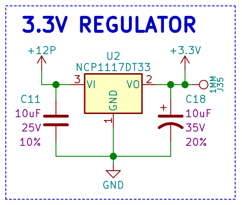
The software has to assume that the reference is perfectly 3.3V, but in reality it can be different from 3.3V. This difference is determined by the worst case accuracy of the external 3.3V reference. The 3.3V reference in our case is a simple Linear Regulator from ON Semiconductor (NCP1117DT33T5G):
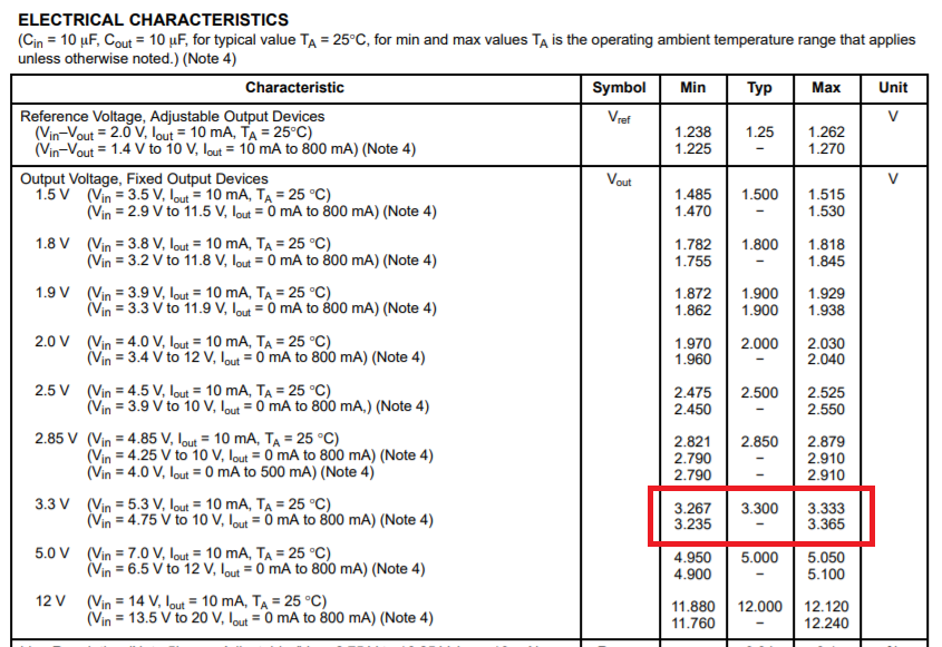
The output voltage range is defined in the datasheet in this section:
With this information we can calculate the worst case output voltage when the reference is at its maximum or minimum output voltage:
Internal 4.096V Reference Worst Case Circuit Analysis
Below is an equation that will be done in SW in order to determine the correct number of Counts to send to the DAC in order to generate 1V:
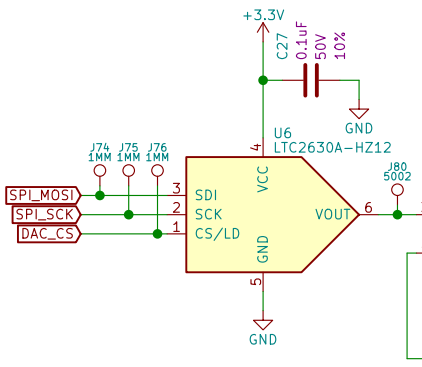
The software has to assume that the reference is perfectly 4.096V, but in reality it can be different from 4.096V. This difference is determined by the worst case accuracy of the internal 4.096V reference. The 4.096V reference in our case is inside the LTC2630 DAC:
"The reference is INSIDE the DAC!" (Zoolander reference, pun intended)
![Image result for zoolander the files are in the computer]()
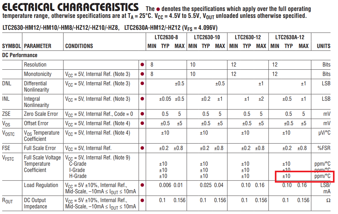
This is where things get hard to compare apples to apples, but the datasheet leads me to believe that the error introduced by the internal reference is specified here in the datasheet for the DAC:
We are designing for a maximum ambient temperature of 70C, therefore the worst case reference error should be around 0.07%. This gives a minimum voltage of 4.093V and a maximum of 4.098V.
With this information we can calculate the worst case output voltage when the reference is at its maximum or minimum output voltage:
As you can see the error is significantly less when using the internal reference of the DAC. Minimizing this error is very important because this DAC Output voltage accuracy will directly translate to load current accuracy. My goal is for this electronic load to be very accurate, therefore I want to enable every option that will increase the accuracy of the load current.
Please note that there are definitely other contributors to DAC Output voltage error, but the premise of this log was to compare the references and their contribution to the error. If you wish to see a more lengthy explanation of an overall worst case analysis of output error, please let me know.
I hope you enjoyed my post. Thank you for reading. Please feel free to leave a comment below.
Thanks again.
-
Digital To Analog Converter Control Using SPI
01/26/2020 at 15:02 • 0 commentsSorry for not posting in a while. I just got back from Iceland, and dumped water all over my laptop. I am excited to give and update after a long trip and a laptop covered in rice.
The next challenge that I want to take on is the Digital To Analog Converter (DAC):
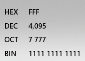
Digital to analog converters are cool devices. DAC's simply output a voltage somewhere between the power and ground reference you provide. The voltage the DAC outputs is based on the message you send it via SPI. This is a 12 bit DAC which means there are the following number of steps:
Therefore we have the following resolution between 3.3V and ground:
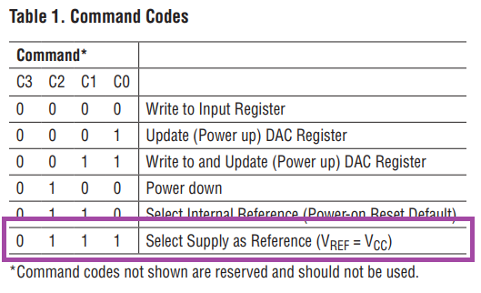
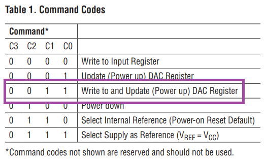
The first thing we are going to do is set the reference voltage to the 3.3V supply we are providing the DAC. This can be done using the following Command Code outlined in the LTC2630 datasheet:
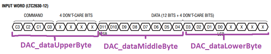
Now that we know the Command Code we need to understand how the rest of the SPI message needs to be structured. The message structure is shown below:
I have broken up the 24 bit message into 3 8-bit variables that I can send in succession.
1. DAC_dataUpperByte_u8
2. DAC_dataMiddleByte_u8
3. DAC_dataLowerByte_u8
For this first message, the DAC is simply going to receive the command code for "Select Supply as Reference" and ignore the rest of the data. Therefore we simply need to package DAC_dataUpperByte with this particular command code, and then send zeros for the remaining bits. The tricky piece is packaging the upper byte. This requires some bit shifting operations. Below is the code that accomplishes this:
uint8_t DAC_selectSupplyAsReferenceCmdCode = 0b0111;

uint8_t DAC_dataUpperByte_u8 = 0b00000000;
uint8_t DAC_dataMiddleByte_u8 = 0b00000000;
uint8_t DAC_dataLowerByte_u8 = 0b00000000;

DAC_dataUpperByte = DAC_selectSupplyAsReferenceCmdCode << 4;
What this code does is takes a uint8_t variable named DAC_dataUpperByte_u8 and sets all bits within the register to 0:
Then we place DAC_selectSupplyAsReferenceCmdCode into DAC_dataUpperByte_u8 register:
Then we shift DAC_selectSupplyAsReferenceCmdCode 4 bits to the left in order to get it into the correct position within the LTC2630 SPI data structure:
Now DAC_dataUpperByte_u8, DAC_dataMiddleByte_u8 & DAC_dataLowerByte_u8 are ready to be sent over the SPI bus from the micro controller to the DAC in order to change the internal reference to our 3.3V supply:
HAL_GPIO_WritePin(DAC_CS_DO_PORT, DAC_CS_DO_PIN, RESET);
HAL_SPI_Transmit(&hspi1, &DAC_dataUpperByte_u8, 1, 10);
HAL_SPI_Transmit(&hspi1, &DAC_dataMiddleByte_u8, 1, 10);
HAL_SPI_Transmit(&hspi1, &DAC_dataLowerByte_u8, 1, 10);
HAL_GPIO_WritePin(DAC_CS_DO_PORT, DAC_CS_DO_PIN, SET);
This code:
1. Pulls the CS pin on the DAC low
2. Sends DAC_dataUpperByte_u8 via SPI
3. Sends DAC_dataMiddleByte_u8 via SPI
4. Sends DAC_dataLowerByte_u8 via SPI
5. Pulls the CS pin the DAC high
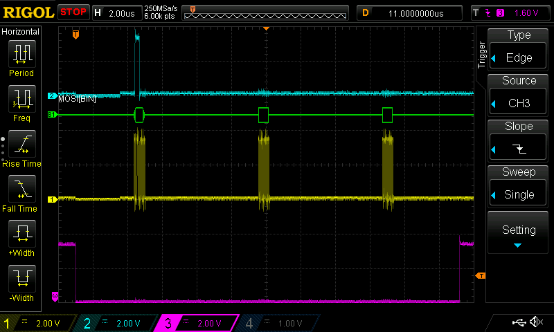
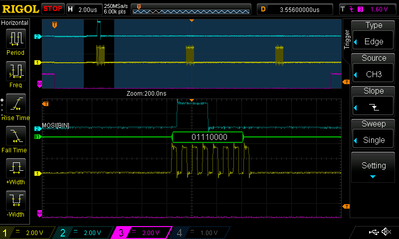
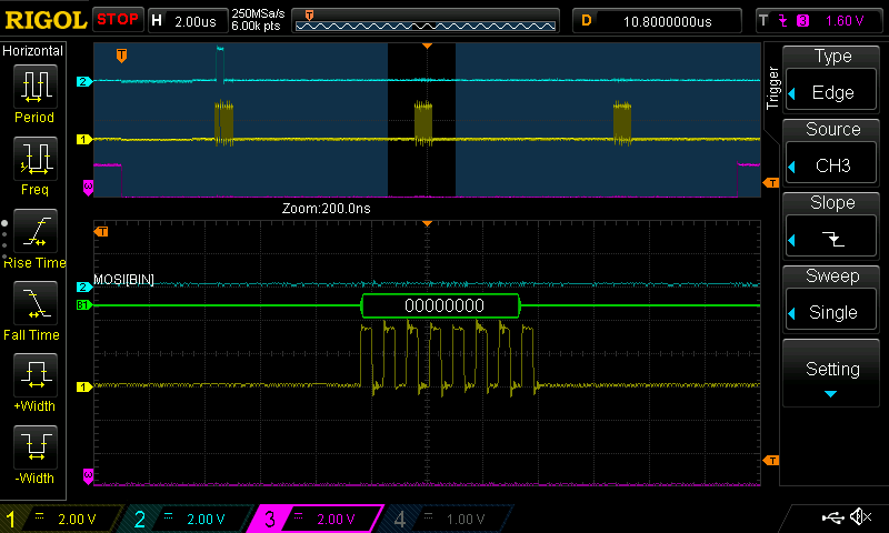
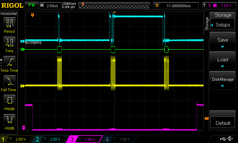
The SPI message can be seen on a scope in the following way:
Upper Byte:
Middle Byte:
Lower Byte:
Now that we have the reference set, we can set a particular output voltage. For this example we will attempt to set the DAC output voltage to 1.95V.
The first thing we need to do is figure out the command code for setting the output voltage:
Luckily we can use the same bit shifting operation for the upper byte.
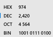
Next we need to figure out the number of counts:
Below is the conversion from 2420 decimal to binary:
This is where things get tricky. We need to take a 12 bit binary message a split it into two bytes named DAC_middleByte_u8 and DAC_lowerByte_u8.
Below is the code for packaging DAC_middleByte_u8:
uint16_t DAC_vSetData_u16 = 0b100101110100;
uint8_t DAC_dataMiddleByte_u8 = 0b00000000;
uint16_t DAC_dataMiddleByte_u16 = 0b0000000000000000;

DAC_dataMiddleByte_u16 = DAC_vSetData_u16 >> 4;
DAC_dataMiddleByte_u8 = DAC_dataMiddleByte_u16;
This code sets DAC_vSetData_u16 with the data to generate 1.95V. Then it initializes an uint8_t DAC_dataMiddleByte_u8 & uint16_t DAC_dataMiddleByte_u16 to a binary value of 0:
Then it takes the contents of DAC_vSetData_u16 and places it inside of DAC_dataMiddleByte_u16:
Then we shift DAC_dataMiddleByte_u16 4 bits to the right in order to get the 8 bits of data we want for DAC_dataMiddleByte_u8 in the first 8 bit positions of DAC_dataMiddleByte_u16:
Now that the relevant data is in the first 8 bits of DAC_dataMiddleByte_u16 we can store its contents into the 8 bit version DAC_dataMiddleByte_u8:
Lastly we need to package DAC_lowerByte_u8. Below is the code for packaging DAC_lowerByte_u8:
uint16_t DAC_vSetData_u16 = 0b100101110100;
uint8_t DAC_dataLowerByte_u8 = 0b00000000;

DAC_dataLowerByte_u8 = DAC_vSetData_u16 & 0b1111;
DAC_dataLowerByte_u8 = DAC_dataLowerByte_u8 << 4;
This uses the same variable DAC_vSetData_u16 with the data to generate 1.95V. Then it initializes an uint8_t DAC_dataLowerByte_u8 to a binary value of 0:
The next step copies the first 4 bits of DAC_vSetData_u16 into the first 4 bits of DAC_dataLowerByte_u8:
Next we shift this data 4 bits to the left in order to match the required data format outlined in the datasheet:
Now DAC_dataUpperByte_u8, DAC_dataMiddleByte_u8 & DAC_dataLowerByte_u8 are ready to be sent over the SPI bus from the micro controller to the DAC in order to change the output voltage to 1.95V. This is the same code we used to set the reference voltage:
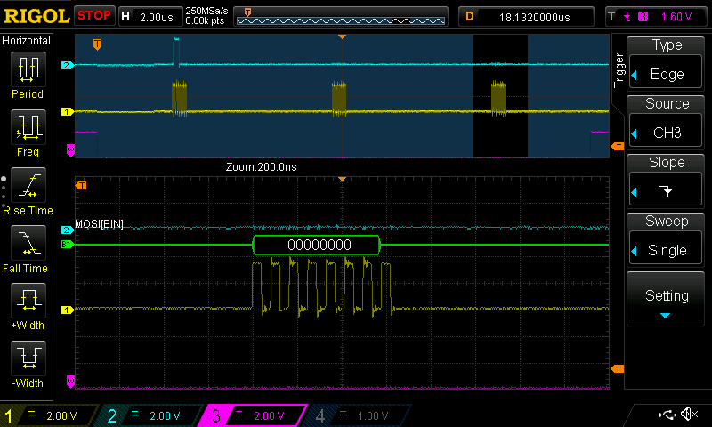
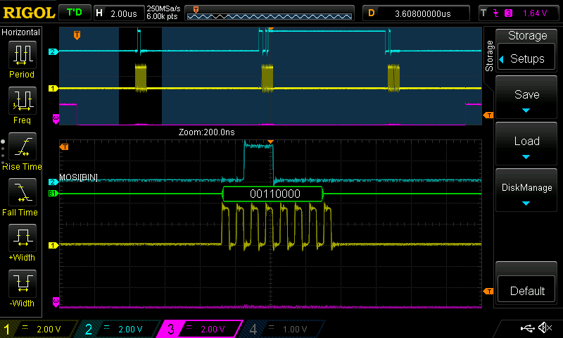
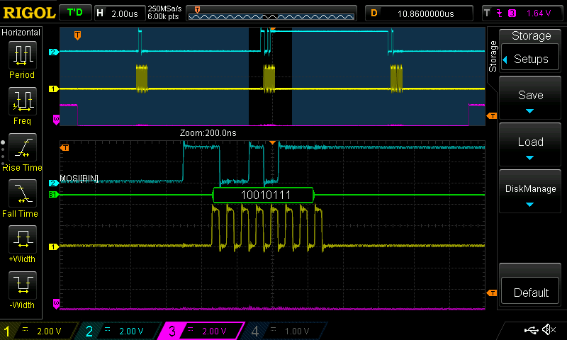
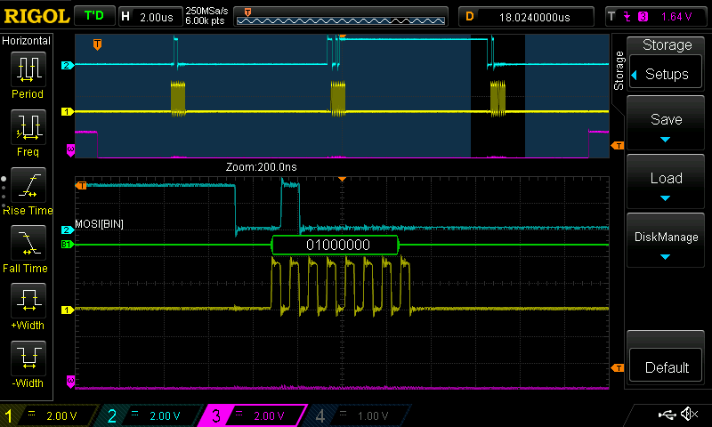
HAL_GPIO_WritePin(DAC_CS_DO_PORT, DAC_CS_DO_PIN, RESET);
HAL_SPI_Transmit(&hspi1, &DAC_dataUpperByte_u8, 1, 10);
HAL_SPI_Transmit(&hspi1, &DAC_dataMiddleByte_u8, 1, 10);
HAL_SPI_Transmit(&hspi1, &DAC_dataLowerByte_u8, 1, 10);
HAL_GPIO_WritePin(DAC_CS_DO_PORT, DAC_CS_DO_PIN, SET);
The SPI message can be seen on a scope in the following way:
Upper Byte:
Middle Byte:
Lower Byte:
To confirm this works we can simply measure the voltage at the output of the DAC to confirm that 1.95V is present:
Now that we have set a single voltage, we can manipulate DAC_vSetData_u16 and change the output voltage of the DAC. I plan on using it to control the MOSFET in order to generate a steady state current. I will cover this in a later post.
I hope you enjoyed my post. Thank you for reading. Please feel free to leave a comment below.
Thanks again.
-
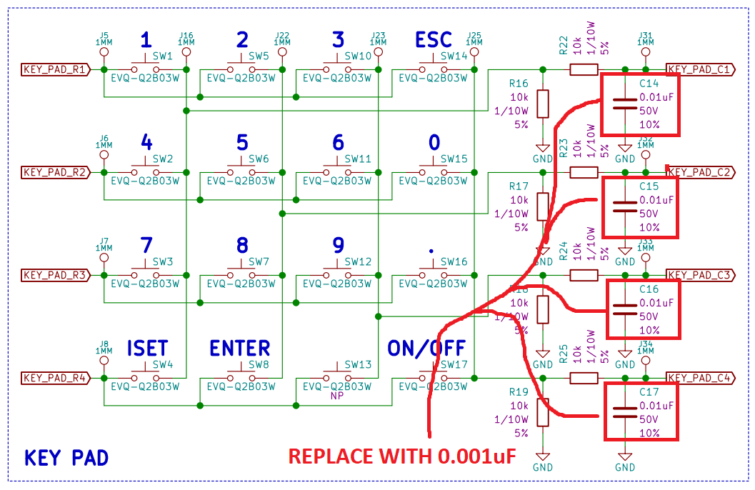
Key Pad Loop Times
01/16/2020 at 23:57 • 0 commentsIn my previous project log I developed a function to read the key pad. In this function there were some necessary delays in order to allow the digital output to fully charge the capacitor on the digital input filter before checking the digital input status (check out more details on the keypad in my previous project log). This delay is based on the RC time constant of the RC low pass filter I have placed in front of each digital input for the key pad.
Below is a visual example of whats happening in the circuit:
You can see that the signal at TP7 and TP23 are instantaneous because there is no deliberate capacitance tied to that node. Therefore the rise and fall times are going to be "instantaneous". The problem is the signal at the digital input is not "instantaneous" because of the resistance/capacitance combination. This resistance/capacitance combination is called a passive low pass filter. Its a cheap and effective way of filtering out unintended high frequencies that you do not want present at your digital input. These high frequencies can come from a number of sources, but typically it is outside RF being coupled into the trace acting like an antenna.
In order to use this low pass filter, we need to wait for the signal to catch up before we read it. This time is based off the RC time constant of the low pass filter. The RC time constant formula is below:
For our circuit we have to consider R as the two 10k resistors, and C as the 0.01uF capacitor. It is best practice to use the worst case value when running an analysis to ensure its compatible across all possible conditions. For this scenario the worst case condition is at the maximum resistance & capacitance values. Our maximum component values are calculated below:
Unfortunately 1T is not enough time since that will only allow the voltage to reach 63% of the steady state value. Its best to wait at least 5T in order for the capacitor in the low pass filter to fully charge before reading the input. This is shown best in the figures below:
Therefore the delay we need to wait after each row is powered is calculated below:
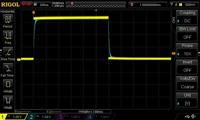
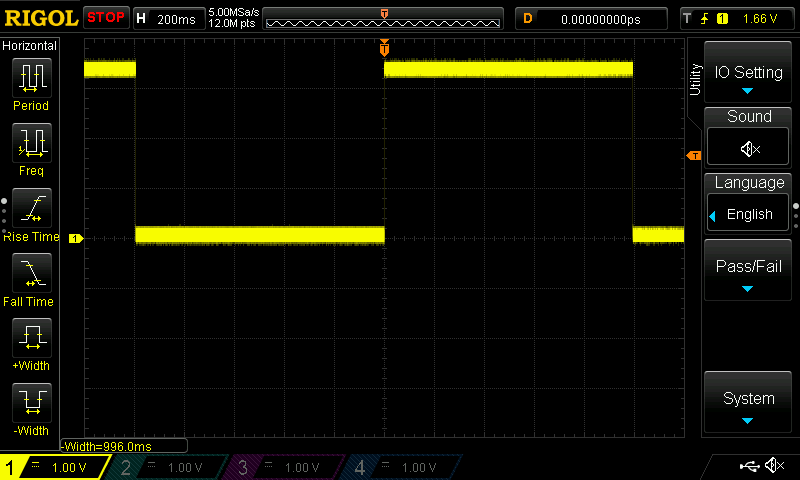
I rounded this value up to an even 1200us and tested the response:
Here you can see the Digital Ouput Voltage (CH1) is instantaneous and the voltage at the Digital Input (CH2) has reached its steady state. This is exactly what you want to see in order to ensure the voltage you we monitoring has reached its steady state.
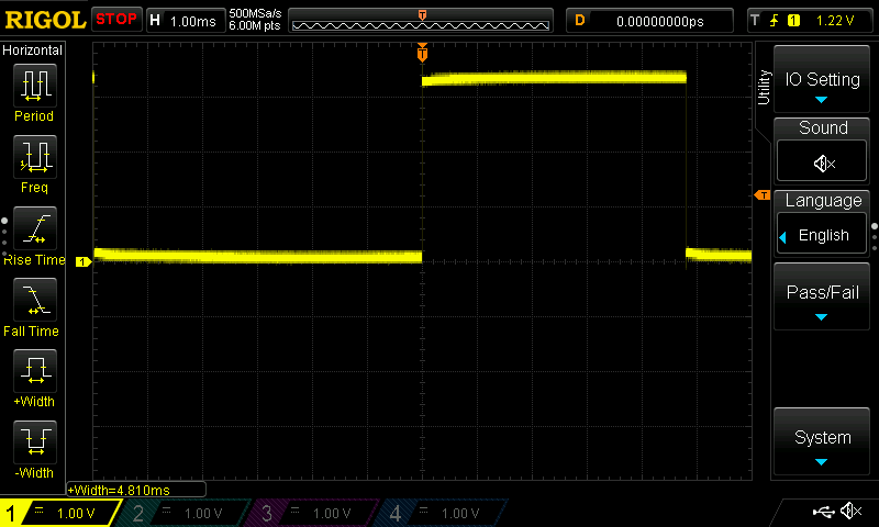
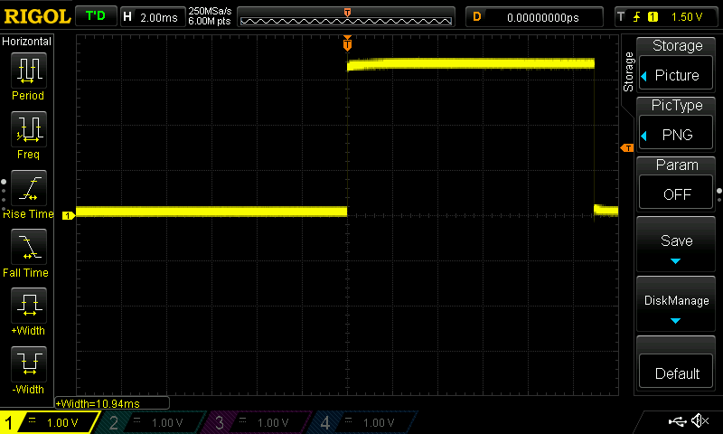
The problem is this takes place 4 times during the readKeyPad() function which gives us a worst case function delay of ~4.8ms. I measured this by executing the following code and taking a measurement on the green LED control:
     if (mainMillis - readKeyPadMillis >= 10)
      {
          turnOnGreenLED();
          readKeyPad();
          turnOffGreenLED();
          readKeyPadMillis = mainMillis;
      }
This function will set the green LED control high, run the readKeyPad() function, and then set the green LED control low. I did this an probed the green LED control to measure the time it takes to execute this function:
As you can see, it takes 4.81ms to execute the readKeyPad() function. This is too long in my opinion, therefore we need to make some HW changes in order to reduce the delays required for this feature. We either need to reduce the low pass filter resistance or capacitance in order to reduce the RC time constant which directly correlates to the required delay. This will move the corner frequency of our low pass filter, but this trade off is definitely worth it. I decided to keep the resistance the same, but to replace the 0.01uF capacitors with 0.001uF capacitors:
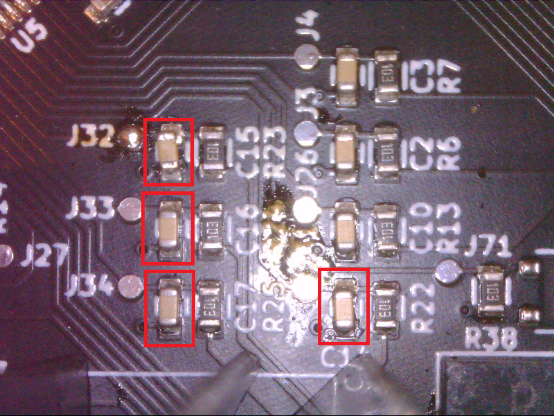
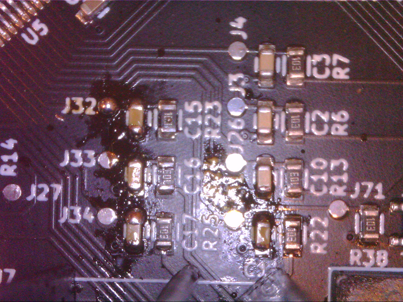
First we had to find C14, C15, C16 & C17 on the PCBA:
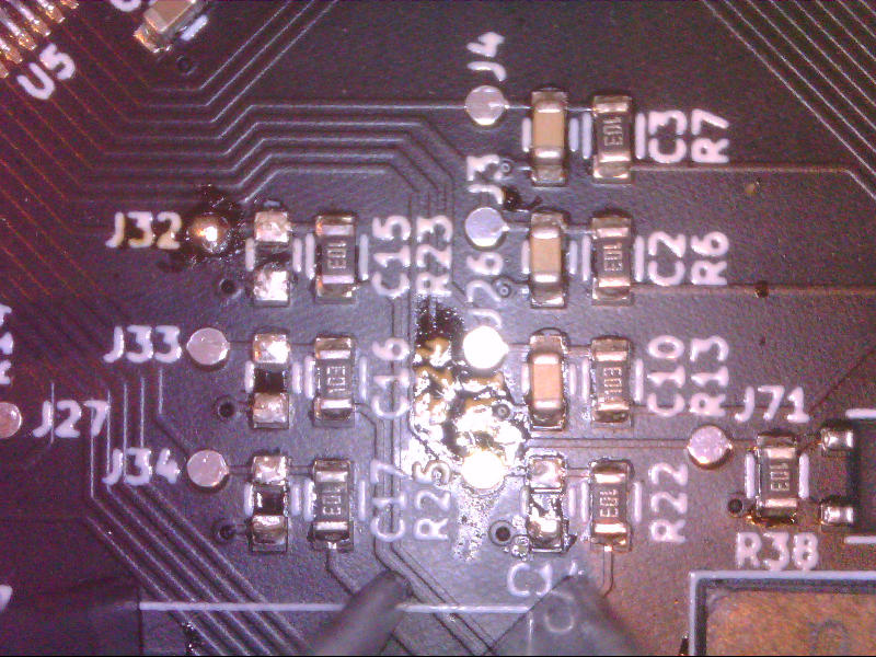
Remove these capacitors from the PCBA:
Solder 0.001uF capacitors:
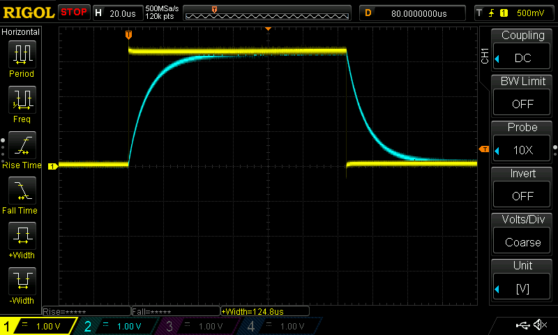
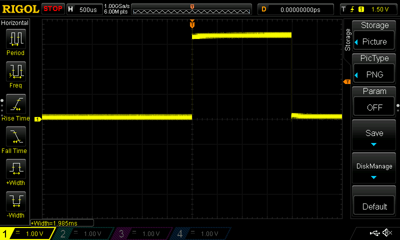
Below is a waveform with the same delay but new capacitors:
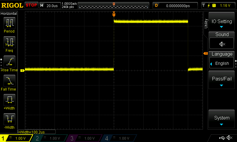
You can see that the 1200us of delay for each digital output is now much longer than we actually need. I adjusted the delay in the SW from 1200us to 120us for each output and go the new response:
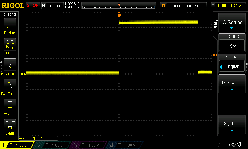
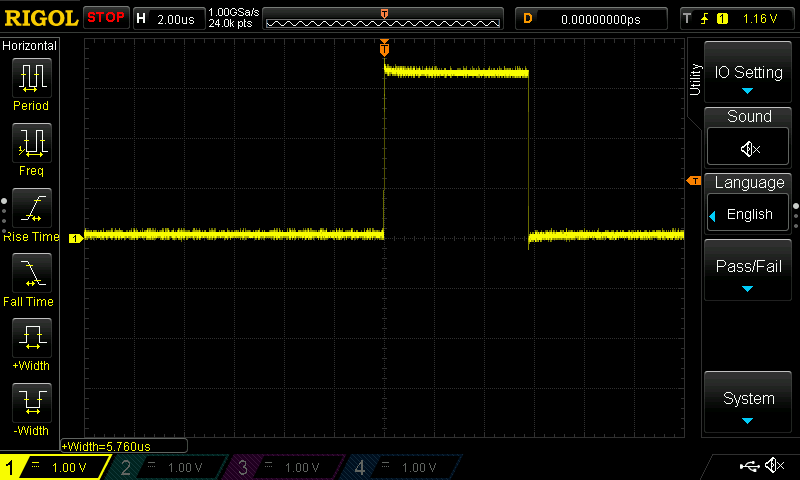
I reran the same test to measure the overall function delay and got the following result:
Now the function only take 511uS to execute, which is much more acceptable.
I hope you enjoyed my post. Thank you for reading. Please feel free to leave a comment below.
Thanks again.
-
Key Pad Fun Times
01/16/2020 at 03:40 • 0 commentsNow that I have figured out digital outputs & delays, the next logical step would be to play with those new features while introducing digital inputs as well. A portion of the design that requires digital output controls, reading digital inputs and delays is the key pad. In order to understand the keypad software, I will give an explanation of the keypad hardware.
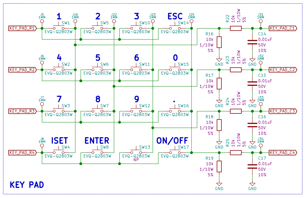
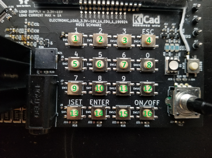
The key pad consists of 16 push buttons:
Schematic View:
PCBA View:
The simplest approach would be to tie all 16 push buttons to a voltage source (3.3V) and route the normally open end of each push button to a discrete digital input. The problem with this approach is it would require 16 GPIO pins on the micro which is a lot for one feature. In order to minimize the required number of GPIO, I used a multiplexed approach which only requires 8 GPIO.
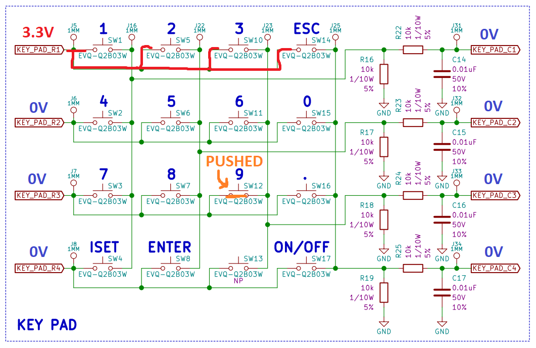
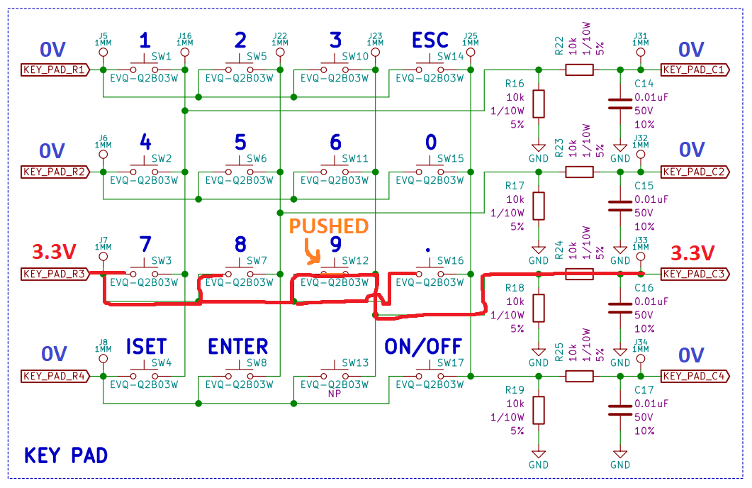
The best way to explain the multiplexed approach is to go through an example. I will show you how the micro-controller will determine that the 9 key (push button 11) is being pushed.
The micro-controller is going to individually power each row, one at a time using digital outputs I named KEY_PAD_R1, KEY_PAD_R2, KEY_PAD_R3 & KEY_PAD_R4. While each row is getting powered individually, the micro-controller is going to check each column one at time using digital inputs I named KEY_PAD_C1, KEY_PAD_C2, KEY_PAD_C3 & KEY_PAD_C4.
When KEY_PAD_R1 digital output is high, this is what the micro-controller will see when the 9 key is pushed:
You can see all digital inputs are reading 0V which is an indication that the 1, 2, 3 or ESC keys are not being pushed.
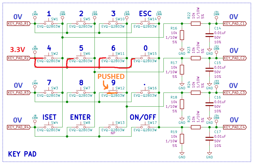
When KEY_PAD_R2 digital output is high, this is what the micro-controller will see when the 9 key is pushed:
You can see all digital inputs are reading 0V which is an indication that the 4, 5, 6 or 0 keys are not being pushed.
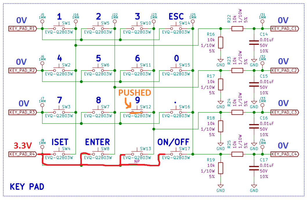
When KEY_PAD_R3 digital output is high, this is what the micro-controller will see when the 9 key is pushed:
You can see in this scenario, the KEY_PAD_C3 digital input is reading 3.3V. The micro will have the 9 key mapped to this condition of KEY_PAD_R3 digital output high & KEY_PAD_C3 digital input high. In fact all keys will have a unique combination that will allow to the micro-controller discretely identify when each key is being pressed.
Lastly when KEY_PAD_R4 digital output is high, this is what the micro-controller will see when the 9 key is pushed:
You can see all digital inputs are reading 0V which is an indication that the ISET, ENTER, NULL or ON/OFF keys are not being pushed.
The logic in the micro-controller can be mapped to this table:
KEY_PAD_R1 Digital Ouput High & KEY_PAD_C1 Digital Input High = 1 Key is pressed
KEY_PAD_R1 Digital Ouput High & KEY_PAD_C2 Digital Input High = 2 Key is pressed
KEY_PAD_R1 Digital Ouput High & KEY_PAD_C3 Digital Input High = 3 Key is pressed
KEY_PAD_R1 Digital Ouput High & KEY_PAD_C4 Digital Input High = ESC Key is pressed
KEY_PAD_R2 Digital Ouput High & KEY_PAD_C1 Digital Input High = 4 Key is pressed
KEY_PAD_R2 Digital Ouput High & KEY_PAD_C2 Digital Input High = 5 Key is pressed
KEY_PAD_R2 Digital Ouput High & KEY_PAD_C3 Digital Input High = 6 Key is pressed
KEY_PAD_R2 Digital Ouput High & KEY_PAD_C4 Digital Input High = 0 Key is pressed
KEY_PAD_R3 Digital Ouput High & KEY_PAD_C1 Digital Input High = 7 Key is pressed
KEY_PAD_R3 Digital Ouput High & KEY_PAD_C2 Digital Input High = 8 Key is pressed
KEY_PAD_R3 Digital Ouput High & KEY_PAD_C3 Digital Input High = 9 Key is pressed
KEY_PAD_R3 Digital Ouput High & KEY_PAD_C4 Digital Input High = . Key is pressed
KEY_PAD_R4 Digital Ouput High & KEY_PAD_C1 Digital Input High = ISET Key is pressed
KEY_PAD_R4 Digital Ouput High & KEY_PAD_C2 Digital Input High = ENTER Key is pressed
KEY_PAD_R4 Digital Ouput High & KEY_PAD_C3 Digital Input High = NULL Key is pressed
KEY_PAD_R4 Digital Ouput High & KEY_PAD_C4 Digital Input High = ON/OFF Key is pressed
I have successfully ported this functionality and logic into a function I called readKeyPad(). This function simply drives the digital outputs, and reads the digital inputs as explained earlier. Based on the digital input readings it knows what button is being pushed. I have introduced a bit of debounce which requires the reading to be successful 5 times in a row before being considered true. If the reading is true then I am simply printing the key number onto the LCD using the LCD_printChar() function I developed in a previous project log.
Another feature I added was a boolean to be set when a key press is identified. When a key press is identified, it will not continue to recognize new key presses until the micro sees that no keys are being pressed. This is to prevent the same key press from being recognized over and over again if the user holds the button down.
Below the code for readKeyPad():
void readKeyPad(void)
{
    HAL_GPIO_WritePin(KEY_PAD_R1_DO_PORT, KEY_PAD_R1_DO_PIN, GPIO_PIN_SET);
    delay_us(1200);
    if (HAL_GPIO_ReadPin(KEY_PAD_C1_DI_PORT, KEY_PAD_C1_DI_PIN) == 1)
    {
        keyPadButtonPressedCount_1 = keyPadButtonPressedCount_1 + 1;
    }
    else if (HAL_GPIO_ReadPin(KEY_PAD_C1_DI_PORT, KEY_PAD_C1_DI_PIN) == 0)
    {
        keyPadButtonPressedCount_1 = 0;
    }

    if (HAL_GPIO_ReadPin(KEY_PAD_C2_DI_PORT, KEY_PAD_C2_DI_PIN) == 1)
    {
        keyPadButtonPressedCount_2 = keyPadButtonPressedCount_2 + 1;
    }
    else if (HAL_GPIO_ReadPin(KEY_PAD_C2_DI_PORT, KEY_PAD_C2_DI_PIN) == 0)
    {
        keyPadButtonPressedCount_2 = 0;
    }

    if (HAL_GPIO_ReadPin(KEY_PAD_C3_DI_PORT, KEY_PAD_C3_DI_PIN) == 1)
    {
        keyPadButtonPressedCount_3 = keyPadButtonPressedCount_3 + 1;
    }
    else if (HAL_GPIO_ReadPin(KEY_PAD_C3_DI_PORT, KEY_PAD_C3_DI_PIN) == 0)
    {
        keyPadButtonPressedCount_3 = 0;
    }

    if (HAL_GPIO_ReadPin(KEY_PAD_C4_DI_PORT, KEY_PAD_C4_DI_PIN) == 1)
    {
        keyPadButtonPressedCount_ESC = keyPadButtonPressedCount_ESC + 1;
    }
    else if (HAL_GPIO_ReadPin(KEY_PAD_C4_DI_PORT, KEY_PAD_C4_DI_PIN) == 0)
    {
        keyPadButtonPressedCount_ESC = 0;
    }
    HAL_GPIO_WritePin(KEY_PAD_R1_DO_PORT, KEY_PAD_R1_DO_PIN, GPIO_PIN_RESET);

    HAL_GPIO_WritePin(KEY_PAD_R2_DO_PORT, KEY_PAD_R2_DO_PIN, GPIO_PIN_SET);
    delay_us(1200);
    if (HAL_GPIO_ReadPin(KEY_PAD_C1_DI_PORT, KEY_PAD_C1_DI_PIN) == 1)
    {
        keyPadButtonPressedCount_4 = keyPadButtonPressedCount_4 + 1;
    }
    else if (HAL_GPIO_ReadPin(KEY_PAD_C1_DI_PORT, KEY_PAD_C1_DI_PIN) == 0)
    {
        keyPadButtonPressedCount_4 = 0;
    }

    if (HAL_GPIO_ReadPin(KEY_PAD_C2_DI_PORT, KEY_PAD_C2_DI_PIN) == 1)
    {
        keyPadButtonPressedCount_5 = keyPadButtonPressedCount_5 + 1;
    }
    else if (HAL_GPIO_ReadPin(KEY_PAD_C2_DI_PORT, KEY_PAD_C2_DI_PIN) == 0)
    {
        keyPadButtonPressedCount_5 = 0;
    }

    if (HAL_GPIO_ReadPin(KEY_PAD_C3_DI_PORT, KEY_PAD_C3_DI_PIN) == 1)
    {
        keyPadButtonPressedCount_6 = keyPadButtonPressedCount_6 + 1;
    }
    else if (HAL_GPIO_ReadPin(KEY_PAD_C3_DI_PORT, KEY_PAD_C3_DI_PIN) == 0)
    {
        keyPadButtonPressedCount_6 = 0;
    }

    if (HAL_GPIO_ReadPin(KEY_PAD_C4_DI_PORT, KEY_PAD_C4_DI_PIN) == 1)
    {
        keyPadButtonPressedCount_0 = keyPadButtonPressedCount_0 + 1;
    }
    else if (HAL_GPIO_ReadPin(KEY_PAD_C4_DI_PORT, KEY_PAD_C4_DI_PIN) == 0)
    {
        keyPadButtonPressedCount_0 = 0;
    }
    HAL_GPIO_WritePin(KEY_PAD_R2_DO_PORT, KEY_PAD_R2_DO_PIN, GPIO_PIN_RESET);

    HAL_GPIO_WritePin(KEY_PAD_R3_DO_PORT, KEY_PAD_R3_DO_PIN, GPIO_PIN_SET);
    delay_us(1200);
    if (HAL_GPIO_ReadPin(KEY_PAD_C1_DI_PORT, KEY_PAD_C1_DI_PIN) == 1)
    {
        keyPadButtonPressedCount_7 = keyPadButtonPressedCount_7 + 1;
    }
    else if (HAL_GPIO_ReadPin(KEY_PAD_C1_DI_PORT, KEY_PAD_C1_DI_PIN) == 0)
    {
        keyPadButtonPressedCount_7 = 0;
    }

    if (HAL_GPIO_ReadPin(KEY_PAD_C2_DI_PORT, KEY_PAD_C2_DI_PIN) == 1)
    {
        keyPadButtonPressedCount_8 = keyPadButtonPressedCount_8 + 1;
    }
    else if (HAL_GPIO_ReadPin(KEY_PAD_C2_DI_PORT, KEY_PAD_C2_DI_PIN) == 0)
    {
        keyPadButtonPressedCount_8 = 0;
    }

    if (HAL_GPIO_ReadPin(KEY_PAD_C3_DI_PORT, KEY_PAD_C3_DI_PIN) == 1)
    {
        keyPadButtonPressedCount_9 = keyPadButtonPressedCount_9 + 1;
    }
    else if (HAL_GPIO_ReadPin(KEY_PAD_C3_DI_PORT, KEY_PAD_C3_DI_PIN) == 0)
    {
        keyPadButtonPressedCount_9 = 0;
    }

    if (HAL_GPIO_ReadPin(KEY_PAD_C4_DI_PORT, KEY_PAD_C4_DI_PIN) == 1)
    {
        keyPadButtonPressedCount_PERIOD = keyPadButtonPressedCount_PERIOD + 1;
    }
    else if (HAL_GPIO_ReadPin(KEY_PAD_C4_DI_PORT, KEY_PAD_C4_DI_PIN) == 0)
    {
        keyPadButtonPressedCount_PERIOD = 0;
    }
    HAL_GPIO_WritePin(KEY_PAD_R3_DO_PORT, KEY_PAD_R3_DO_PIN, GPIO_PIN_RESET);

    HAL_GPIO_WritePin(KEY_PAD_R4_DO_PORT, KEY_PAD_R4_DO_PIN, GPIO_PIN_SET);
    delay_us(1200);
    if (HAL_GPIO_ReadPin(KEY_PAD_C1_DI_PORT, KEY_PAD_C1_DI_PIN) == 1)
    {
        keyPadButtonPressedCount_ISET = keyPadButtonPressedCount_ISET + 1;
    }
    else if (HAL_GPIO_ReadPin(KEY_PAD_C1_DI_PORT, KEY_PAD_C1_DI_PIN) == 0)
    {
        keyPadButtonPressedCount_ISET = 0;
    }

    if (HAL_GPIO_ReadPin(KEY_PAD_C2_DI_PORT, KEY_PAD_C2_DI_PIN) == 1)
    {
        keyPadButtonPressedCount_ENTER = keyPadButtonPressedCount_ENTER + 1;
    }
    else if (HAL_GPIO_ReadPin(KEY_PAD_C2_DI_PORT, KEY_PAD_C2_DI_PIN) == 0)
    {
        keyPadButtonPressedCount_ENTER = 0;
    }

    if (HAL_GPIO_ReadPin(KEY_PAD_C3_DI_PORT, KEY_PAD_C3_DI_PIN) == 1)
    {
        keyPadButtonPressedCount_NULL = keyPadButtonPressedCount_NULL + 1;
    }
    else if (HAL_GPIO_ReadPin(KEY_PAD_C3_DI_PORT, KEY_PAD_C3_DI_PIN) == 0)
    {
        keyPadButtonPressedCount_NULL = 0;
    }

    if (HAL_GPIO_ReadPin(KEY_PAD_C4_DI_PORT, KEY_PAD_C4_DI_PIN) == 1)
    {
        keyPadButtonPressedCount_ONOFF = keyPadButtonPressedCount_ONOFF + 1;
    }
    else if (HAL_GPIO_ReadPin(KEY_PAD_C4_DI_PORT, KEY_PAD_C4_DI_PIN) == 0)
    {
        keyPadButtonPressedCount_ONOFF = 0;
    }
    HAL_GPIO_WritePin(KEY_PAD_R4_DO_PORT, KEY_PAD_R4_DO_PIN, GPIO_PIN_RESET);

    if ((keyPadButtonPressedCount_1 == 0) && (keyPadButtonPressedCount_2 == 0) && (keyPadButtonPressedCount_3 == 0) && (keyPadButtonPressedCount_ESC == 0)
            && (keyPadButtonPressedCount_4 == 0) && (keyPadButtonPressedCount_5 == 0) && (keyPadButtonPressedCount_6 == 0) && (keyPadButtonPressedCount_0 == 0)
            && (keyPadButtonPressedCount_7 == 0) && (keyPadButtonPressedCount_8 == 0) && (keyPadButtonPressedCount_9 == 0) && (keyPadButtonPressedCount_PERIOD == 0)
            && (keyPadButtonPressedCount_ISET == 0) && (keyPadButtonPressedCount_ENTER == 0) && (keyPadButtonPressedCount_NULL == 0) && (keyPadButtonPressedCount_ONOFF == 0))
    {
        keyPadButtonPressedCount_NONE = keyPadButtonPressedCount_NONE + 1;
    }
    else if (HAL_GPIO_ReadPin(KEY_PAD_C1_DI_PORT, KEY_PAD_C1_DI_PIN) == 0)
    {
        keyPadButtonPressedCount_NONE = 0;
    }

    if ((keyPadButtonPressedCount_1 == 5)  && (buttonPressed==false))
    {
        LCD_printChar("1");
        buttonPressed = true;
    }
    else if ((keyPadButtonPressedCount_2 == 5)  && (buttonPressed==false))
    {
        LCD_printChar("2");
        buttonPressed = true;
    }
    else if ((keyPadButtonPressedCount_3 == 5)  && (buttonPressed==false))
    {
        LCD_printChar("3");
        buttonPressed = true;
    }
    else if ((keyPadButtonPressedCount_ESC == 5)  && (buttonPressed==false))
    {
        LCD_printChar("ESC");
        buttonPressed = true;
    }
    else if ((keyPadButtonPressedCount_4 == 5)  && (buttonPressed==false))
    {
        LCD_printChar("4");
        buttonPressed = true;
    }
    else if ((keyPadButtonPressedCount_5 == 5)  && (buttonPressed==false))
    {
        LCD_printChar("5");
        buttonPressed = true;
    }
    else if ((keyPadButtonPressedCount_6 == 5)  && (buttonPressed==false))
    {
        LCD_printChar("6");
        buttonPressed = true;
    }
    else if ((keyPadButtonPressedCount_0 == 5)  && (buttonPressed==false))
    {
        LCD_printChar("0");
        buttonPressed = true;
    }
    else if ((keyPadButtonPressedCount_7 == 5)  && (buttonPressed==false))
    {
        LCD_printChar("7");
        buttonPressed = true;
    }
    else if ((keyPadButtonPressedCount_8 == 5)  && (buttonPressed==false))
    {
        LCD_printChar("8");
        buttonPressed = true;
    }
    else if ((keyPadButtonPressedCount_9 == 5)  && (buttonPressed==false))
    {
        LCD_printChar("9");
        buttonPressed = true;
    }
    else if ((keyPadButtonPressedCount_PERIOD == 5)  && (buttonPressed==false))
    {
        LCD_printChar(".");
        buttonPressed = true;
    }
    else if ((keyPadButtonPressedCount_ISET == 5)  && (buttonPressed==false))
    {
        LCD_printChar("ISET");
        buttonPressed = true;
    }
    else if ((keyPadButtonPressedCount_ENTER == 5)  && (buttonPressed==false))
    {
        LCD_printChar("ENTER");
        buttonPressed = true;
    }
    else if ((keyPadButtonPressedCount_NULL == 5)  && (buttonPressed==false))
    {
        LCD_printChar("NULL");
        buttonPressed = true;
    }
    else if ((keyPadButtonPressedCount_ONOFF == 5)  && (buttonPressed==false))
    {
        LCD_printChar("ONOFF");
        buttonPressed = true;
    }
    else if ((keyPadButtonPressedCount_NONE == 5)  && (buttonPressed==true))
    {
        buttonPressed = false;
    }
    return;
}
I am running through this function every 10ms using the millis() function I developed in previous project log:
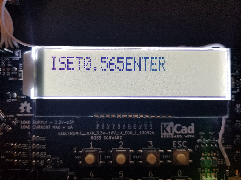
      if (mainMillis - readKeyPadMillis >= 10)
      {
          readKeyPad();
          readKeyPadMillis = mainMillis;
      }
To test, I hit ISET then typed 0.56 followed by the ENTER key all while looping some other functions in the background:
Using the key pad feels great. I had a few other people test it out and they felt the response was good and very user friendly.
One last thing to note is the delay required after each digital output is set high. This is needed in order for the filter capacitor in front of the digital input to fully charge to steady state before reading the digital input. I realized when writing the code that this delay is a little too long for my liking, therefore I plan to update the HW design in order to reduce this required delay. I will be covering this topic in my next project log.
I hope you enjoyed my post. Thank you for reading. Please feel free to leave a comment below.
Thanks again.
-
Millis Function
01/13/2020 at 02:38 • 0 commentsIn order to avoid large pockets of delay, I will need to generate a function that will allow me to execute specific actions only after a certain amount of time has expired. In arduino, this can be accomplished using the millis() function. Since I am using the STM32 micro-controller and the STM32 IDE, I do not have the luxury of using this library function. Therefore I have created my own millis function. Probably not as good, but seems to be working pretty well.
The first step was to enable a new timer that counts up at a rate of 100kHz (In other words it counts to 100 every 1ms):
static void MX_TIM7_Init(void)
{
  htim7.Instance = TIM7;
  htim7.Init.Prescaler = 479; //479
  htim7.Init.CounterMode = TIM_COUNTERMODE_UP;
  htim7.Init.Period = 65535;
  htim7.Init.AutoReloadPreload = TIM_AUTORELOAD_PRELOAD_DISABLE;
  if (HAL_TIM_Base_Init(&htim7) != HAL_OK)
  {
    Error_Handler();
  }
}
This function configures a timer to count up to 100 every 1ms. The reason I have slowed down this timer is to prevent the 16 bit unsigned integer from over flowing too quickly. This timer can overflow after following duration:
Once all of my code is complete, I can start to bench mark the amount of time it takes to execute the entire stack. With that information I can fine tune my timer frequency, but for now I will conservatively set the frequency to 100kHz.
Now that I have a timer that counts to 100 every 1ms, I have created a function that counts how many times this happens:
uint32_t millis(void)
{
    uint16_t CURRENT_TIMER7_COUNT = __HAL_TIM_GET_COUNTER(&htim7);

    uint16_t currentMillis = 0;
    if(CURRENT_TIMER7_COUNT>=100)
    {
        currentMillis = CURRENT_TIMER7_COUNT/100;
        systemMillis = systemMillis + currentMillis;
        __HAL_TIM_SET_COUNTER (&htim7, 0);
    }
    return systemMillis;
}
This function checks the current count at the time this function is called. If the count is larger than 100 it increases a variable called systemMillis by 1. systemMillis is the current number of milliseconds the application has been running. If the counter is increased it resets the counter to prevent it from overflowing. systemMillis is a 32 bit unsigned integer which will take a long time to over flow. The systemMillis variable will overflow after this specified amount of time:
This is an acceptable amount of time to run this particular application with requiring a reset. Once this timer expires I plan on resetting all the Millis related variables which might cause a slight timing mishap, but should not be noticeable to the user if the user has left application running longer than 49.71 days.
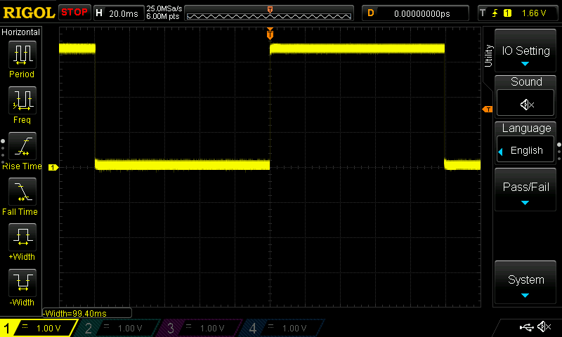
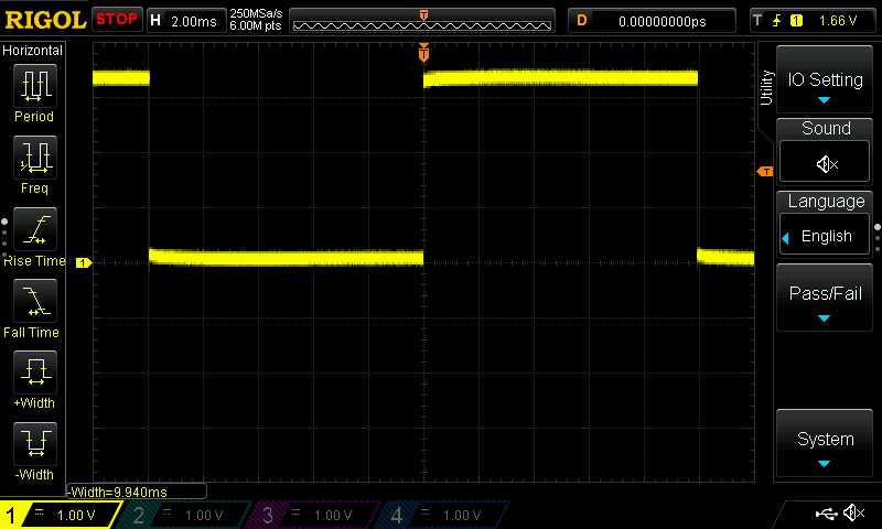
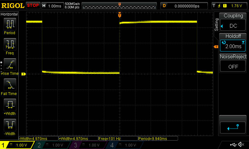
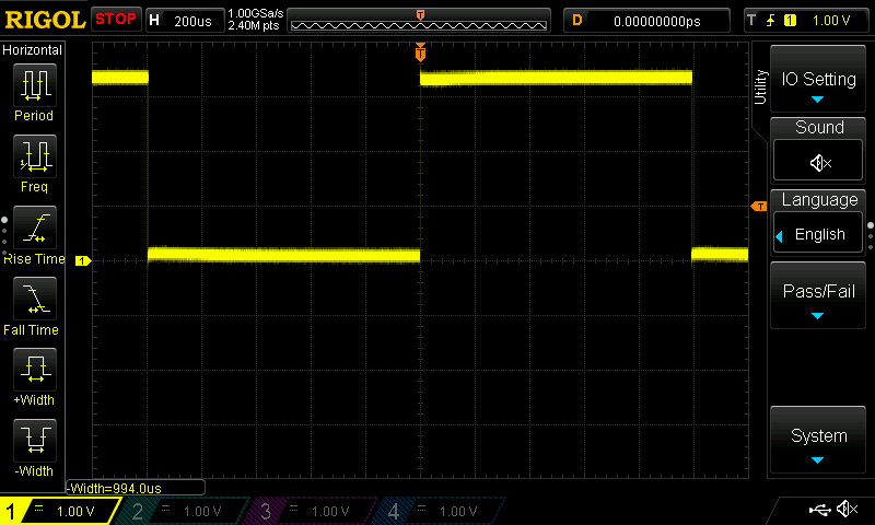
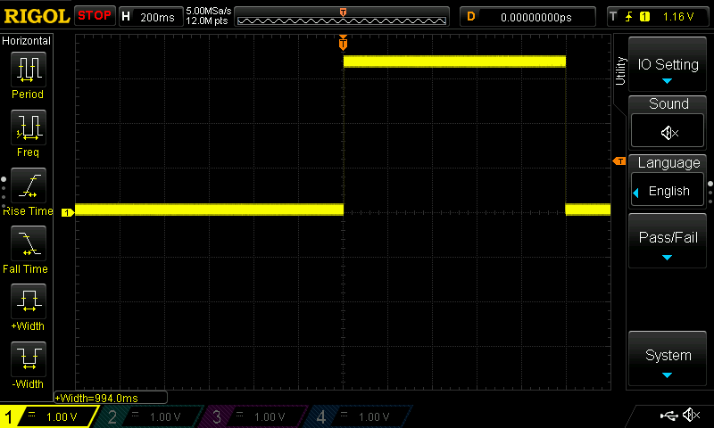
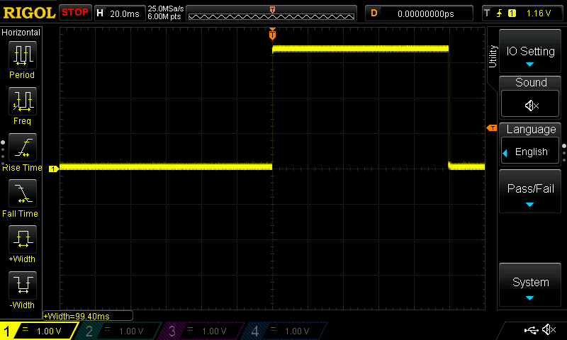
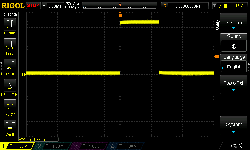
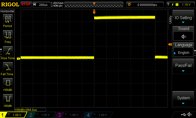
I then tested this function within main while(1) by blinking an LED on and off and probing the LED DO port:
mainMillis = millis();

if (mainMillis - turnOnRedLedMillis >= 1000)
{
    HAL_GPIO_TogglePin(DEBUG_RGB_LED_R_DO_PORT, DEBUG_RGB_LED_R_DO_PIN);
    turnOnRedLedMillis = mainMillis;
}
1s:
100ms:
10ms:
5ms:
1ms:
These results are adequate for my needs. This new function will help me execute portions of the code only when they really need to be execute. I think this will be most useful for low priority portions of the code being executed less then portions that are higher priority.
There are many uses for this function and you will be sure to see it future updates regarding SW.
Hope you found this interesting, and if you have any ideas that would work better please let me know. Thank you for reading.
-
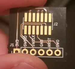
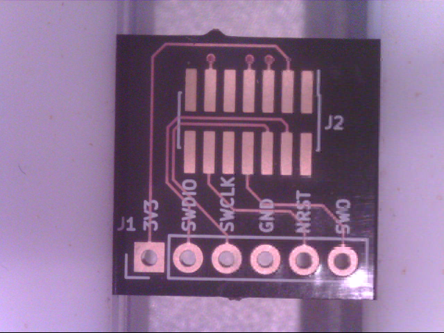
Programming Header Simplification
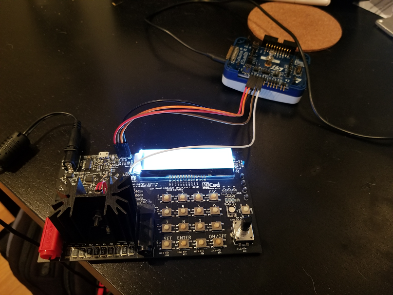
12/21/2019 at 04:53 • 0 commentsI have been getting annoyed with my current programming header connections:
The connections need to be individually un-done and re-done if you want to disconnect the programming tool from the PCB. Therefor i have decided to make an adapter board that would make my programming interface directly compatible with the main 14 pin header on the STLINK-V3:
![Image result for st link v3]()
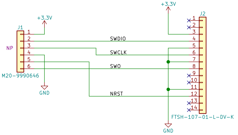
Below is the schematic I created:
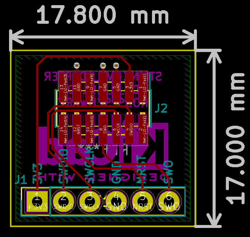
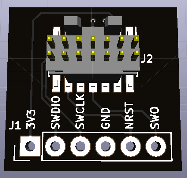
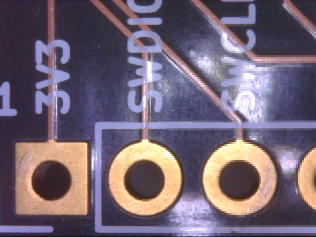
Below is the board I designed:
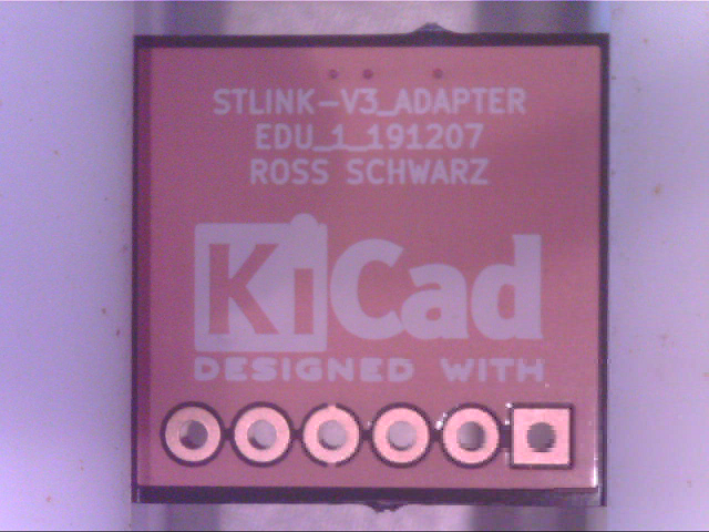
I ordered these boards on OSH Park, and took advantage of the cool "After Dark" option that is currently available:
This board construction is really cool because it uses a dark substrate and a clear soldermask. This makes it look like the copper is exposed, but it is in fact under a layer of clear solder resist material.
The construction on these boards is really incredible. The copper etching and silk screen definition is insanely good.
I then soldered the connector to the board, and this jumper board to my PCB:
I then connected to the STLINK-V3 using the 14 way ribbon cable as mentioned earlier:
After a quick test, I was able to connect to my micro-controller and successfully flash the micro-controller. This makes disconnecting and reconnecting the STLINK-V3 much easier. This also cleans up my bench setup as well.
Hope you found this interesting. Thanks for reading.
-
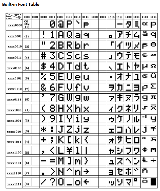
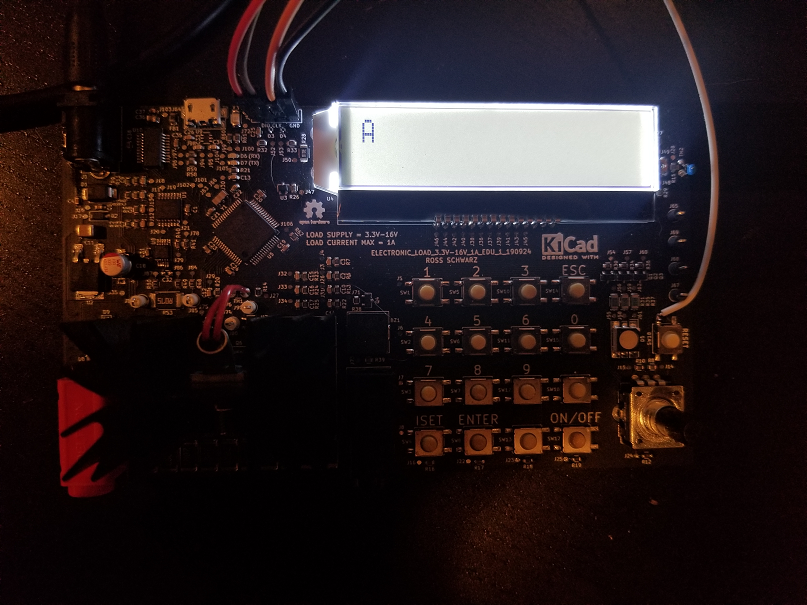
Hello World - LCD Edition
12/19/2019 at 02:57 • 0 commentsThe LCD when powered looks so cool, lets make it say something now!
This has definitely been the hardest part yet, and will most likely be a work in progress as the SW matures. Later versions are going to take a number of inputs and map them onto the display to show information related to the electronic load performance. For now I simply want to create a function that will print a string onto the LCD. I started by generating functions to initialize the LCD functionality:
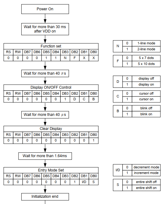
void LCD_functionSet(void)
{
    HAL_GPIO_WritePin(GPIOA, GPIO_PIN_15, GPIO_PIN_RESET);    //RS
    HAL_GPIO_WritePin(GPIOC, GPIO_PIN_10, GPIO_PIN_RESET);    //RW

    HAL_GPIO_WritePin(GPIOB, GPIO_PIN_8, GPIO_PIN_RESET);    //DB7
    HAL_GPIO_WritePin(GPIOB, GPIO_PIN_7, GPIO_PIN_RESET);    //DB6
    HAL_GPIO_WritePin(GPIOB, GPIO_PIN_6, GPIO_PIN_SET);        //DB5
    HAL_GPIO_WritePin(GPIOB, GPIO_PIN_5, GPIO_PIN_SET);        //DB4

    HAL_GPIO_WritePin(GPIOB, GPIO_PIN_4, GPIO_PIN_SET);        //DB3
    HAL_GPIO_WritePin(GPIOB, GPIO_PIN_3, GPIO_PIN_RESET);    //DB2
    HAL_GPIO_WritePin(GPIOD, GPIO_PIN_2, GPIO_PIN_RESET);    //DB1
    HAL_GPIO_WritePin(GPIOC, GPIO_PIN_12, GPIO_PIN_RESET);    //DB0

    HAL_GPIO_WritePin(GPIOC, GPIO_PIN_11, GPIO_PIN_SET);    //E
    delay_us(1);
    HAL_GPIO_WritePin(GPIOC, GPIO_PIN_11, GPIO_PIN_RESET);    //E
    delay_us(40);
    return;
}

void LCD_displayOnOffControl(void)
{
    HAL_GPIO_WritePin(GPIOA, GPIO_PIN_15, GPIO_PIN_RESET);    //RS
    HAL_GPIO_WritePin(GPIOC, GPIO_PIN_10, GPIO_PIN_RESET);    //RW

    HAL_GPIO_WritePin(GPIOB, GPIO_PIN_8, GPIO_PIN_RESET);    //DB7
    HAL_GPIO_WritePin(GPIOB, GPIO_PIN_7, GPIO_PIN_RESET);    //DB6
    HAL_GPIO_WritePin(GPIOB, GPIO_PIN_6, GPIO_PIN_RESET);    //DB5
    HAL_GPIO_WritePin(GPIOB, GPIO_PIN_5, GPIO_PIN_RESET);    //DB4

    HAL_GPIO_WritePin(GPIOB, GPIO_PIN_4, GPIO_PIN_SET);        //DB3
    HAL_GPIO_WritePin(GPIOB, GPIO_PIN_3, GPIO_PIN_SET);        //DB2
    HAL_GPIO_WritePin(GPIOD, GPIO_PIN_2, GPIO_PIN_RESET);    //DB1
    HAL_GPIO_WritePin(GPIOC, GPIO_PIN_12, GPIO_PIN_RESET);    //DB0

    HAL_GPIO_WritePin(GPIOC, GPIO_PIN_11, GPIO_PIN_SET);    //E
    delay_us(1);
    HAL_GPIO_WritePin(GPIOC, GPIO_PIN_11, GPIO_PIN_RESET);    //E
    delay_us(40);
    return;
}

void LCD_clearDisplay(void)
{
    HAL_GPIO_WritePin(GPIOA, GPIO_PIN_15, GPIO_PIN_RESET);    //RS
    HAL_GPIO_WritePin(GPIOC, GPIO_PIN_10, GPIO_PIN_RESET);    //RW

    HAL_GPIO_WritePin(GPIOB, GPIO_PIN_8, GPIO_PIN_RESET);    //DB7
    HAL_GPIO_WritePin(GPIOB, GPIO_PIN_7, GPIO_PIN_RESET);    //DB6
    HAL_GPIO_WritePin(GPIOB, GPIO_PIN_6, GPIO_PIN_RESET);    //DB5
    HAL_GPIO_WritePin(GPIOB, GPIO_PIN_5, GPIO_PIN_RESET);    //DB4

    HAL_GPIO_WritePin(GPIOB, GPIO_PIN_4, GPIO_PIN_RESET);    //DB3
    HAL_GPIO_WritePin(GPIOB, GPIO_PIN_3, GPIO_PIN_RESET);    //DB2
    HAL_GPIO_WritePin(GPIOD, GPIO_PIN_2, GPIO_PIN_RESET);    //DB1
    HAL_GPIO_WritePin(GPIOC, GPIO_PIN_12, GPIO_PIN_SET);    //DB0

    HAL_GPIO_WritePin(GPIOC, GPIO_PIN_11, GPIO_PIN_SET);    //E
    delay_us(1);
    HAL_GPIO_WritePin(GPIOC, GPIO_PIN_11, GPIO_PIN_RESET);    //E
    delay_ms(2);
    return;
}

void LCD_entryModeSet(void)
{
    HAL_GPIO_WritePin(GPIOA, GPIO_PIN_15, GPIO_PIN_RESET);    //RS
    HAL_GPIO_WritePin(GPIOC, GPIO_PIN_10, GPIO_PIN_RESET);    //RW

    HAL_GPIO_WritePin(GPIOB, GPIO_PIN_8, GPIO_PIN_RESET);    //DB7
    HAL_GPIO_WritePin(GPIOB, GPIO_PIN_7, GPIO_PIN_RESET);    //DB6
    HAL_GPIO_WritePin(GPIOB, GPIO_PIN_6, GPIO_PIN_RESET);    //DB5
    HAL_GPIO_WritePin(GPIOB, GPIO_PIN_5, GPIO_PIN_RESET);    //DB4

    HAL_GPIO_WritePin(GPIOB, GPIO_PIN_4, GPIO_PIN_RESET);    //DB3
    HAL_GPIO_WritePin(GPIOB, GPIO_PIN_3, GPIO_PIN_SET);        //DB2
    HAL_GPIO_WritePin(GPIOD, GPIO_PIN_2, GPIO_PIN_SET);        //DB1
    HAL_GPIO_WritePin(GPIOC, GPIO_PIN_12, GPIO_PIN_RESET);    //DB0

    HAL_GPIO_WritePin(GPIOC, GPIO_PIN_11, GPIO_PIN_SET);    //E
    delay_us(1);
    HAL_GPIO_WritePin(GPIOC, GPIO_PIN_11, GPIO_PIN_RESET);    //E
    delay_us(40);
    return;
}
Now that I have initialized the LCD, I can send commands for the different characters and it will print the characters onto:
I started with a function to print the letter A:
void LCD_print_A(void)
{
    HAL_GPIO_WritePin(GPIOA, GPIO_PIN_15, GPIO_PIN_SET);    //RS
    HAL_GPIO_WritePin(GPIOC, GPIO_PIN_10, GPIO_PIN_RESET);    //RW

    HAL_GPIO_WritePin(GPIOB, GPIO_PIN_8, GPIO_PIN_RESET);    //DB7
    HAL_GPIO_WritePin(GPIOB, GPIO_PIN_7, GPIO_PIN_SET);        //DB6
    HAL_GPIO_WritePin(GPIOB, GPIO_PIN_6, GPIO_PIN_RESET);    //DB5
    HAL_GPIO_WritePin(GPIOB, GPIO_PIN_5, GPIO_PIN_RESET);    //DB4

    HAL_GPIO_WritePin(GPIOB, GPIO_PIN_4, GPIO_PIN_RESET);    //DB3
    HAL_GPIO_WritePin(GPIOB, GPIO_PIN_3, GPIO_PIN_RESET);    //DB2
    HAL_GPIO_WritePin(GPIOD, GPIO_PIN_2, GPIO_PIN_RESET);    //DB1
    HAL_GPIO_WritePin(GPIOC, GPIO_PIN_12, GPIO_PIN_SET);    //DB0

    HAL_GPIO_WritePin(GPIOC, GPIO_PIN_11, GPIO_PIN_SET);    //E
    delay_us(1);
    HAL_GPIO_WritePin(GPIOC, GPIO_PIN_11, GPIO_PIN_RESET);    //E
    delay_us(40);
    return;
}
I ran a simple combo of these functions in main to test the functionality:
LCD_print_A();
delay_ms(1000);
LCD_clearDisplay();
I made similar functions for the other letters of the alphabet, along with space and key punctuation. The next part is deconstructing a string and printing each letter individually. Below is the function I created to accomplish this:
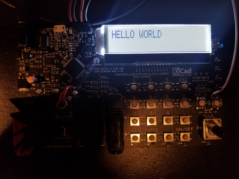
void LCD_printString(char string[])
{
    char stringInitial[21] = "";
    char stringCopied[21] = "";
    char* stringPointer;
    uint16_t i = 0;

    strcpy(stringInitial, string);

    uint16_t stringLength = strlen(stringInitial);

    //UART_printlnString(&huart2, stringInitial);

    while(i < stringLength)
    {
        stringPointer = &stringInitial[i];
        memcpy(stringCopied, stringPointer, 1);

        if(strcmp(stringCopied," ") == 0)
        {
            LCD_print_SPACE();
        }
        else if(strcmp(stringCopied,".") == 0)
        {
            LCD_print_PERIOD();
        }
        else if(strcmp(stringCopied,"/") == 0)
        {
            LCD_print_FWDSLASH();
        }
        else if(strcmp(stringCopied,"0") == 0)
        {
            LCD_print_0();
        }
        else if(strcmp(stringCopied,"1") == 0)
        {
            LCD_print_1();
        }
        else if(strcmp(stringCopied,"2") == 0)
        {
            LCD_print_2();
        }
        else if(strcmp(stringCopied,"3") == 0)
        {
            LCD_print_3();
        }
        else if(strcmp(stringCopied,"4") == 0)
        {
            LCD_print_4();
        }
        else if(strcmp(stringCopied,"5") == 0)
        {
            LCD_print_5();
        }
        else if(strcmp(stringCopied,"6") == 0)
        {
            LCD_print_6();
        }
        else if(strcmp(stringCopied,"7") == 0)
        {
            LCD_print_7();
        }
        else if(strcmp(stringCopied,"8") == 0)
        {
            LCD_print_8();
        }
        else if(strcmp(stringCopied,"9") == 0)
        {
            LCD_print_9();
        }
        else if(strcmp(stringCopied,"A") == 0)
        {
            LCD_print_A();
        }
        else if(strcmp(stringCopied,"B") == 0)
        {
            LCD_print_B();
        }
        else if(strcmp(stringCopied,"C") == 0)
        {
            LCD_print_C();
        }
        else if(strcmp(stringCopied,"D") == 0)
        {
            LCD_print_D();
        }
        else if(strcmp(stringCopied,"E") == 0)
        {
            LCD_print_E();
        }
        else if(strcmp(stringCopied,"F") == 0)
        {
            LCD_print_F();
        }
        else if(strcmp(stringCopied,"G") == 0)
        {
            LCD_print_G();
        }
        else if(strcmp(stringCopied,"H") == 0)
        {
            LCD_print_H();
        }
        else if(strcmp(stringCopied,"I") == 0)
        {
            LCD_print_I();
        }
        else if(strcmp(stringCopied,"J") == 0)
        {
            LCD_print_J();
        }
        else if(strcmp(stringCopied,"K") == 0)
        {
            LCD_print_K();
        }
        else if(strcmp(stringCopied,"L") == 0)
        {
            LCD_print_L();
        }
        else if(strcmp(stringCopied,"M") == 0)
        {
            LCD_print_M();
        }
        else if(strcmp(stringCopied,"N") == 0)
        {
            LCD_print_N();
        }
        else if(strcmp(stringCopied,"O") == 0)
        {
            LCD_print_O();
        }
        else if(strcmp(stringCopied,"P") == 0)
        {
            LCD_print_P();
        }
        else if(strcmp(stringCopied,"Q") == 0)
        {
            LCD_print_Q();
        }
        else if(strcmp(stringCopied,"R") == 0)
        {
            LCD_print_R();
        }
        else if(strcmp(stringCopied,"S") == 0)
        {
            LCD_print_S();
        }
        else if(strcmp(stringCopied,"T") == 0)
        {
            LCD_print_T();
        }
        else if(strcmp(stringCopied,"U") == 0)
        {
            LCD_print_U();
        }
        else if(strcmp(stringCopied,"V") == 0)
        {
            LCD_print_V();
        }
        else if(strcmp(stringCopied,"W") == 0)
        {
            LCD_print_W();
        }
        else if(strcmp(stringCopied,"X") == 0)
        {
            LCD_print_X();
        }
        else if(strcmp(stringCopied,"Y") == 0)
        {
            LCD_print_Y();
        }
        else if(strcmp(stringCopied,"Z") == 0)
        {
            LCD_print_Z();
        }

        //UART_printlnString(&huart2, stringCopied);
        i = i + 1;
    }
    return;
}
This function takes a string, and looks at each character one by one. If the character matches a known character in the "if statement", then it prints that character onto the display. The while loop goes through each character until it has gone through the entire string length.
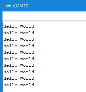
Running the following function with "HELLO WORLD" gets the following result:
LCD_printString("HELLO WORLD"); delay_ms(1000); LCD_clearDisplay(); -
Hello World - UART Edition
12/19/2019 at 02:04 • 2 commentsThe next goal for me is to get my UART running. This will be a huge accomplishment since using a serial monitor is going to be very helpful when debugging code. I found two really helpful functions online which allow you to pass a character array (char) and it will send the string via the defined UART interface:
void UART_printString(UART_HandleTypeDef *huart, char _out[])
{
    HAL_UART_Transmit(huart, (uint8_t *) _out, strlen(_out), 10);
}

void UART_printlnString(UART_HandleTypeDef *huart, char _out[])
{
    HAL_UART_Transmit(huart, (uint8_t *) _out, strlen(_out), 10);
    char newline[2] = "\r\n";
    HAL_UART_Transmit(huart, (uint8_t *) newline, 2, 10);
}
I plugged in my USB connection and passed a simple "Hello World" string into the UART_printlnString() function:
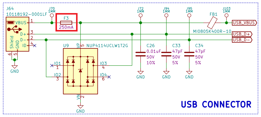
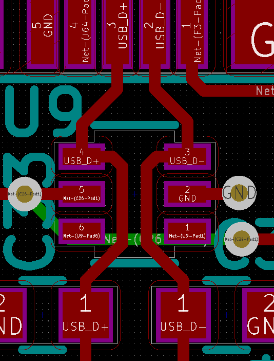
UART_printlnString(&huart2,"Hello World");
delay_ms(1000);
Unfortunately this did not work right away. Through some quick trouble shooting, I noticed the USB VBUS fuse F3 had blown open:
I knew this to be the case because I could measure 5V at J70 when connected to my computer, but J72 was reading ~0V. After some head scratching, I looked into the details of my USB ESD protection U9 a bit further. What I noticed is my silk screen did not have any pin 1 identification, and this device definitely needs to be oriented correctly when soldered:
After some further investigation, I did in fact solder D9 backwards which results in a forward biased diode directly from VBUS to ground through fuse F3. I corrected the issue by simply removing D9 for now, and replacing F3 with a new fuse. (I will be fixing the silkscreen in future revisions of the PCB)
After this change I got the re-assuring ba-da-da-boo from my PC that it recognized a USB device was plugged in.
I opened my serial monitor and wah lah:
-
Delays
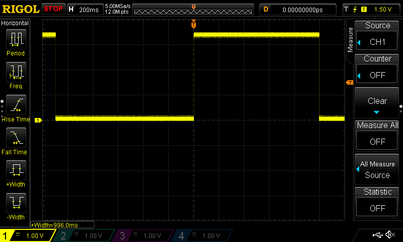
12/13/2019 at 00:45 • 0 commentsOne of the first things I do in a SW project is identify the delay functions I wish to use, and test them. I have not used and STM32 mico before, therefore I am going to test the performance of the HAL_Delay() function:
HAL_GPIO_WritePin(GPIOA, GPIO_PIN_9, GPIO_PIN_SET);
HAL_Delay(1000);
HAL_GPIO_WritePin(GPIOA, GPIO_PIN_9, GPIO_PIN_RESET);
HAL_Delay(1000);
I measured each delay pulse width using a scope at 1s, 100ms, 10ms, 5ms & 1ms.
1s:
![]()
100ms:
![]()
10ms:
![]()
5ms:
![]()
1ms:
![]()
At longer delays >100ms I really like the HAL_Delay() function. At lower delays <10ms I noticed there is nearly a +1ms error that may add a significant amount of overall delay if used often. Also there is no option to go into a microsecond time frame which will definitely be necessary when writing functions for the LCD. When driving the LCD, every character write requires a 40us delay, but if using the HAL_Delay(1), it would cause the following overall delay:
This is a lot of delay for one type of feature, therefore I generated a micro second delay using an internal timer:
void delay_us(uint16_t delay){
    delay = delay * 48;
    __HAL_TIM_SET_COUNTER (&htim6, 0);
    while (__HAL_TIM_GET_COUNTER(&htim6) < delay);
}
This function takes an integer (number of microseconds) multiplies it by 48. Then it resets timer 6, and timer 6 starts counting up at 48MHz. Therefore the timer counts to 48 in 1us. The while loop waits until it counts all the way up to the limit and then returns back to where the function was called. I made the same measurements on my delay_us() function.
100us:
![]()
10us:
![]()
5us:
![]()
1us:
![]()
I am really happy with the delay_us() function. Also I created a delay_ms function:
void delay_ms(uint16_t delay){
    while(delay > 0){
        delay_us(1000);
        delay = delay - 1;
    }
}
This function simply takes an integer, and runs through delay_us(1000) that number of times. Pretty simple. Below are the measurements results:
1s:
![]()
100ms:
![]()
10ms:
![]()
5ms:
![]()
1ms:
![]()
I am very happy with the accuracy of the delay_ms() function as well. I can be confident how long certain delays should be now that I understand and have measured these delays.
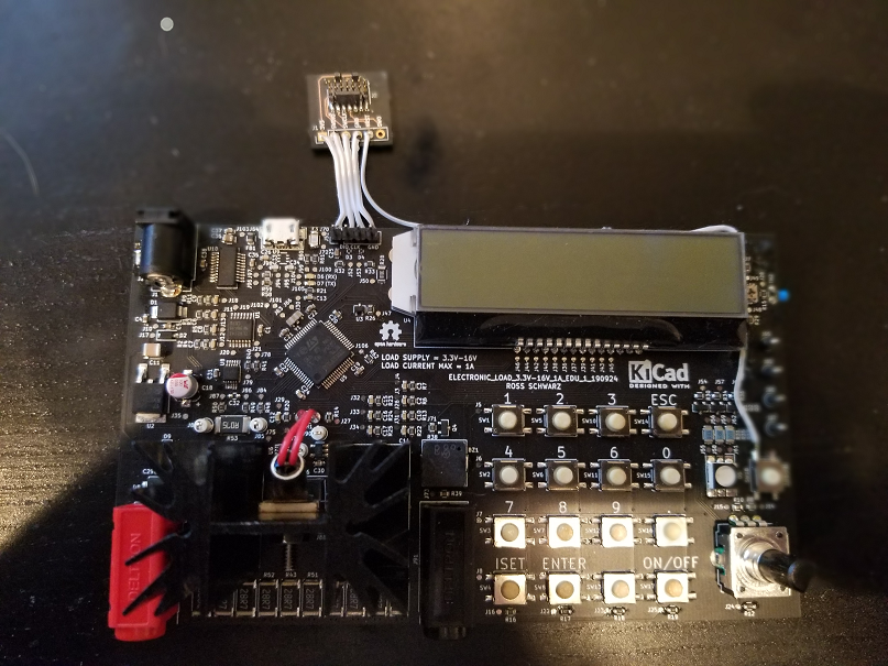
Electronic Load 3.3V-16V 1A
Electronic load that supports 3.3V-16V at 1A of current. Equipped with keypad, LCD, rotary encoder, STM32 Microcontroller and more!