Close
0%
0%

Smart WiFi Home Light Switch

IoT light switch using ESP 32 WiFI module

Similar projects worth following
This is a prototype project I developed during my spare time. I want to challenge myself to create a small and compact IoT device that can be mounted inside a conventional light switch socket and change all most every light to IoT lights. Currently, the most device on the market with the same capability sells around $60 -$100. Lower price range smart light switches have little to none programming flexibility and often drops commands due to interference.

I started this project because I want to learn more and grow more as an engineer. This project includes multiple aspects of engineering: AC-DC power converters, microcontroller bring up and configuration, firmware programming, mobile app user interface, and mechanical design.

It is an ambitious project for one person. However, I believe knowledge should be shared instead of withholding for one's own interest. I will open-source all the schematics and code for everyone who might find those helpful.

Flyback Converter Design

The Flyback converter will provide a 120 VAC to 5VDC power conversion. The ESP32 requires 3.3V power input. Therefore a Low-dropout regulator (LDO) will be used to convert 5V to 3.3V for the microcontroller to use. This linear regulator would also reduce ripples created by the flyback converter and provide a clean power supply for our controller to use.
There are many ways to convert AC to DC, but the Flyback converter is the most popular and cost-efficient way to do so. Plus, the flyback transformer will provide isolation between AC and DC. This isolation helps to reduce noise propagating between AC and DC and Electromagnetic interference. 

Microcontroller ESP32

ESP 32 has WiFi, Bluetooth, capacitance touch sensor, ADC, DAC and hall effect sensor functionality built-in and yet sells around $5 per chip. Even with the WiFi PCB antenna build-in, it only cost me $5.88 each. 

Switching the light

The light switching would be a high voltage rating relay. The microcontroller would control this relay base on the sensors reading and WiFi communication sent from the cloud server. 

Sensors

In this project, I am trying to test a temperature sensor and a motion sensor. The reliability of the sensor reading under an AC present environment would be investigated. 

Schamtics and PCB file are in Github
https://github.com/Charingchen/Smart-Light-Switch-PCB

  • 1 × ESP32-WROOM-32
  • 1 × UCC28704

  • Flyback Converter Circuit Design

    Charing Chen02/04/2020 at 23:19 0 comments

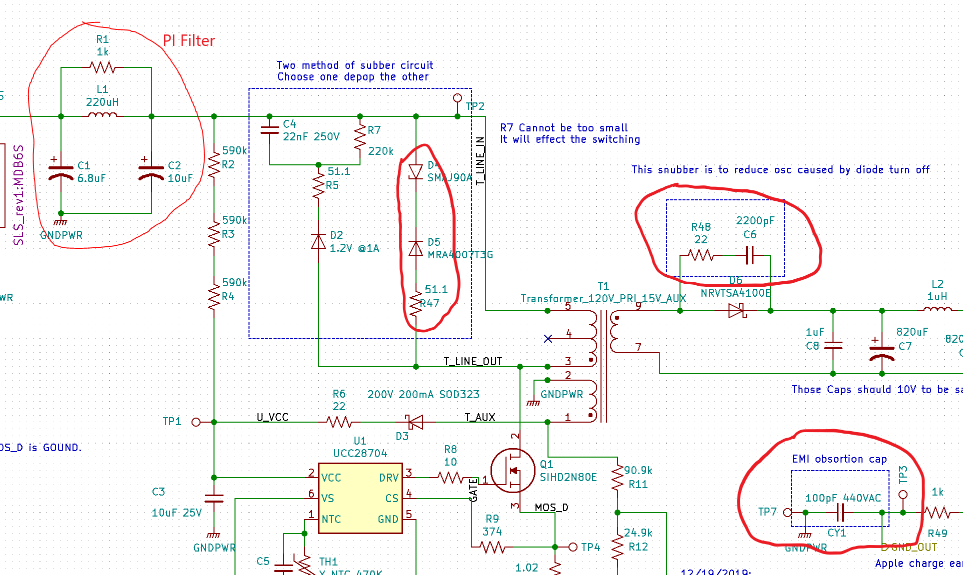
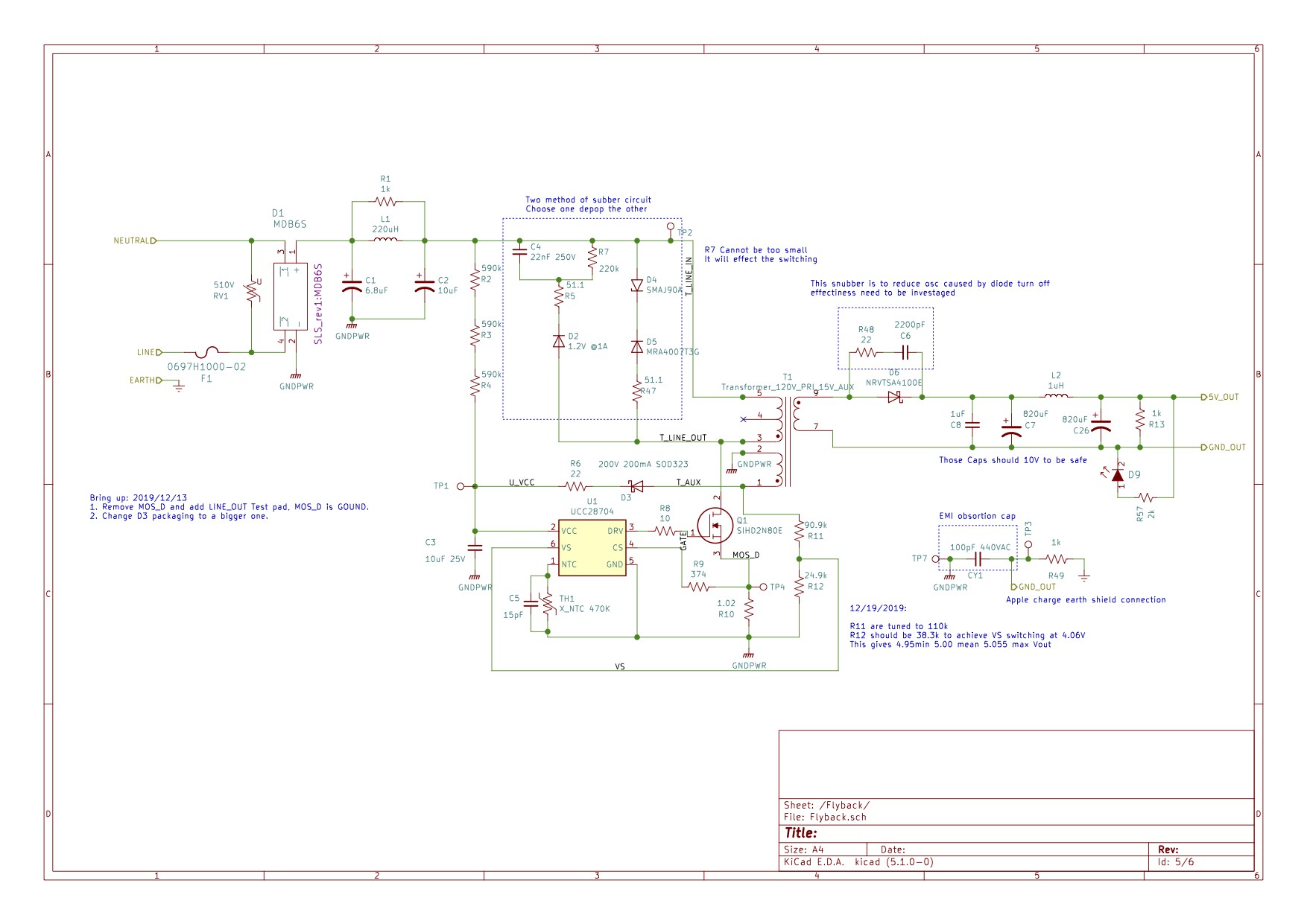
    Here is the finalized circuit I have built and tested working for 120VAC. Let's go through the circuit component one by one.

    Control chip

    The control chip I used is UCC28704, which is a low cost and low part requirement chip from Texas Instruments. Highlight feature includes voltage valley skipping and no optical coupler required.

    Simplfied Schematic for UCC28704

    Voltage valley skipping reduces the ringing caused by the MOSFET switch turning off. Less voltage ringing would reduce EMI.

    UCC28704 uses the AUX winding instead of the optical coupler to provide voltage feedback. Every stable system requires feedback. The Traditional and most common flyback converter uses an optical coupler to give control feedback from its output rail. This part does not have a long life and is often broken due to the optical part wear out fast. 

    Startup power of the chip

    This is a smart way to power up the control chip by using a third set of windings called AUX windings. In my design, this would give out about 15V at AUX. However, when the system starts from zero, the aux would not have voltage since there is no switching yet, therefore, the chip needs to get its initial power directly from line input which is around 160VDC. This line voltage is reduced by a series of large resistors before feeding into the chip. Once it gets the initial juice to start operating the MOSFET, the AUX winding will start to have voltage and through a diode, only and a positive portion would be powering the chip now.

    There is a more efficient way of this startup circuit. If the designer is aiming for higher efficiency to achieve a better power rating, for example, 80 plus Gold power ratting, one should consider this circuit to reduce start-up power loss and shorten the startup time. Instead of a series of resistance constant couple on the Vblk, a depletion-mode FET would connect the V blk when starting from no power and disconnect when ucc28704 is powered. This is controlled by one of the chips pin called NTC/SU, this would source a 105uA current when the chip is powered. Therefore, when the Qst2 has not current from the chip would result in qst1 be on. Vis versa.  Detailed circuit please reference to 7.3.6.2 in the datasheet.

    Regulation and feedback

    Any stable system requires feedback to know if it is hitting its target. Without feedback, it would be blindfold and walking in the dark. Especially with an electrical system, without feedback, it would often result in a dramatic, loud and smoky outcome. 

    In this circuit, the feedback is done via the Auxiliary winding. Instead of an optical coupler, which has a low life cycle often fail before all other parts, Auxiliary winding will copy exactly behaviour as our output does, but with different voltage level. The controller chip will use this auxiliary reading to know to switch "harder" or idle for a brief moment. So that no overvoltage nor under-voltage at the output.

    EMI

    EMI is also a critical consideration when designing any power converter. In the circuit diagram, you will see Pi filters, Y capacitor connecting Power ground and output ground; snubber circuit to absorb the sudden change of voltage to reduce electromagnetic noise.

    To be a commercialized product, all power converter has to pass Federal Communications Commission (FCC) in North America and CISPR in the European region. 

    The Pi filter I selected comes from a reference design of a similar 5V power converter. Since this stage I would not commercialize my board, I don’t have to go through lab testing on the effectiveness of my pi filter. Those emission tests require a radio frequency free environment and a lot of expensive equipment to achieve. 

    However, out of curiosity, I have some measurement on the effectiveness of the snubber circuit:

    The Results show the TVS snubber circuit indeed drops maximum voltage peak on the line voltage after rectifier (Blue) from 736V to 352V and reduce 5V peak voltage from 5.8V - 5.55V ( This is before the...

    Read more »

View project log

Enjoy this project?

Share

Discussions

Not-Lazy-Dev wrote 12/31/2020 at 01:56 point

Where can I find the schematic and stuff?

  Are you sure? yes | no

Similar Projects

Does this project spark your interest?

Become a member to follow this project and never miss any updates