-
Finishing touches
05/03/2020 at 17:15 • 0 commentsI thought i called it a wrap on this project, but there were still a few small things to investigate. Here are the changes I made, which now puts things in a finished state.
Increase switching frequency to 120 kHz. At 100 kHz, the peak current on the transformer primary side would exceed its saturation rating (3 A). In DCM, the peak current is independent of the input voltage. Based on an load current of 30 mA, 120 kHz provides a better solution for keeping the primary-side current within datasheet limits.
Changes to current sense network: increase R_sense to 33 mΩ and remove R_SL (use a 0 Ω jumper). DCM is stable without an artificial ramp, but simulations showed the converter can drop into CCM for transients at low input voltage. Unfortunately, there is no combination of R_sense and R_SL that simultaneously limit the peak current to 3 A and guarantee stability in CCM at this low frequency, while respecting the 2 kΩ limit on R_SL. The biggest transient is at startup, and CCM operation can be prevented there with a generous soft-start time. Simulations showed effects on the load-step transients were tolerable, so I decided to use a R_sense, R_SL network that would solve for the peak current limit only. As a consequence, it's expected the output voltage will droop when the load current exceeds 30 mA as the LM5155 is limiting the current to protect the transformer core from saturating. The lower switching frequency also means a larger filter capacitor is possible, so C11 was increased to 22 nF.
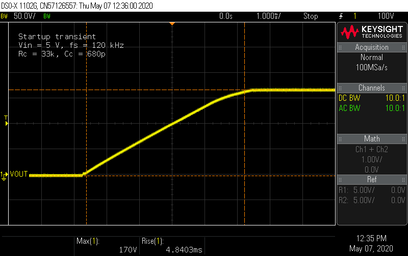
Increase soft-start capacitor to 47 nF. Simulations showed a longer startup time keeps the converter out of CCM during startup. This choice more than doubles the startup ramp time to about 5 ms.

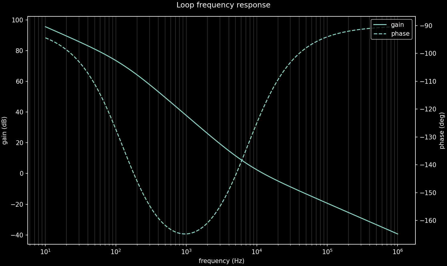
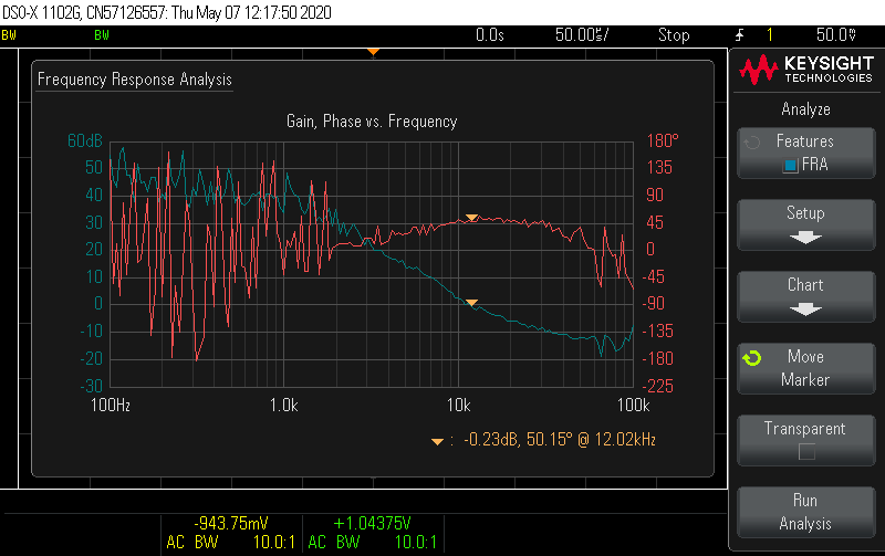
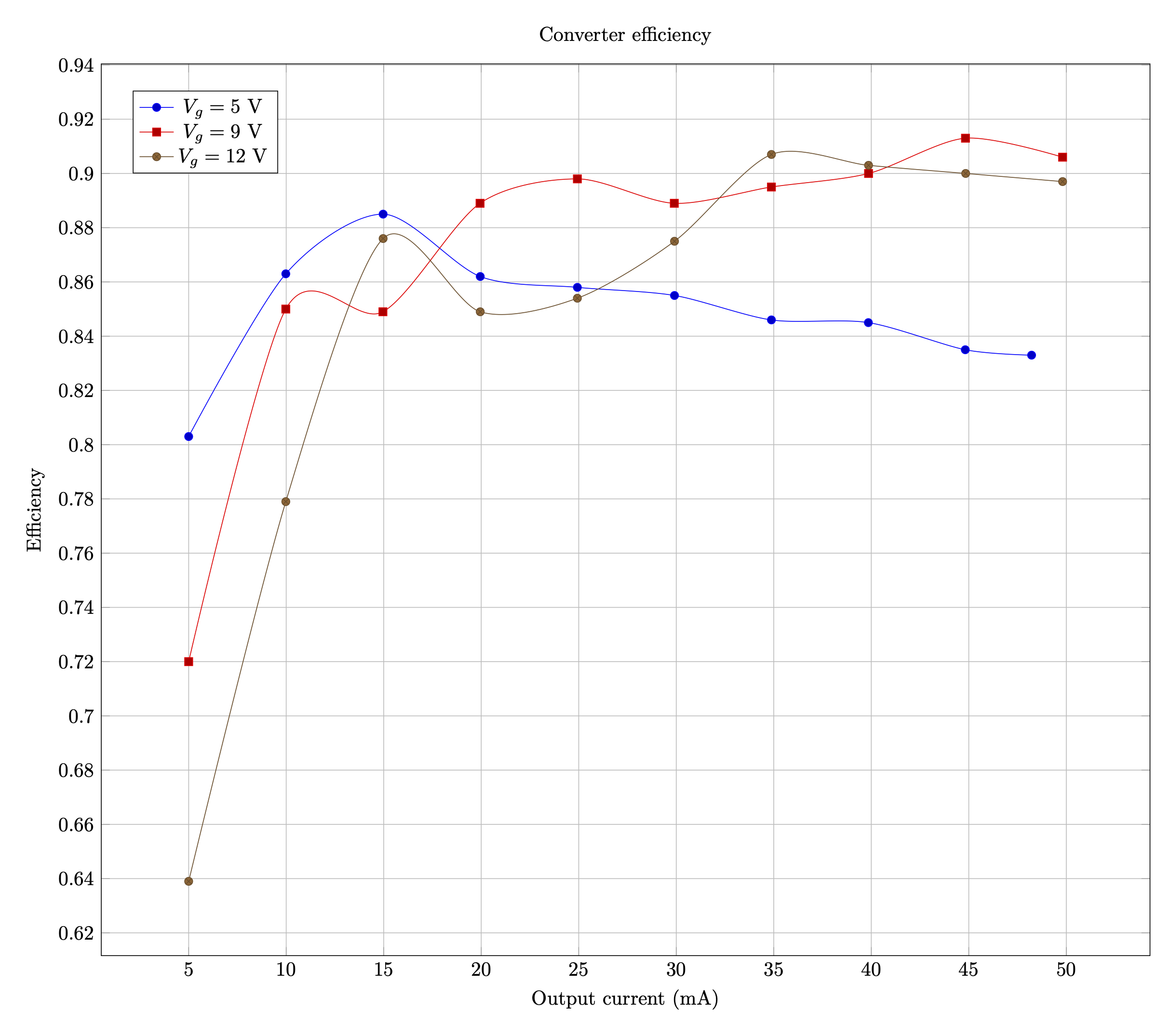
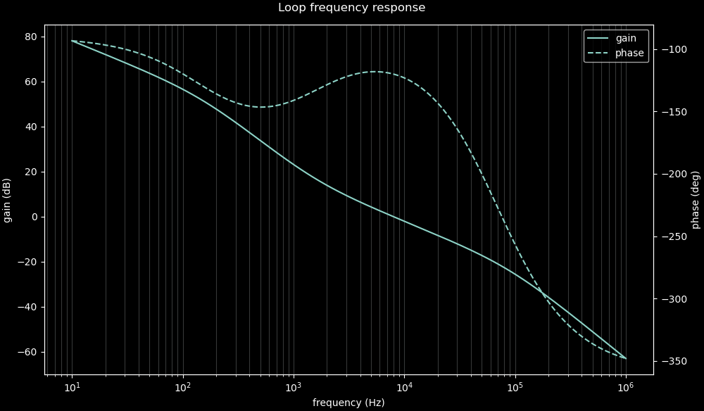
Improve compensation network. I derived an analytical small-signal model of the flyback in DCM-CPM, which informed better choices of the compensation network. I also made an error in the previous script and forgot to include the PWM gain factor (parenthetically referenced in tiny text on the LM5155 datasheet ... thanks TI). In DCM, the low-frequency behavior of the loop is approximately a single-pole system, with identical gain and pole frequency to a buck-boost controller. Without a RHP zero in the model, there is no obvious and natural choice for a HF pole, so I removed the second capacitor and used R = 33 kΩ and C = 680 pF to set the crossover at 12 kHz with 60° phase margin. These charts show the predicted and measured results. The converter now reacts to 5 mA load steps so fast, it wasn't even possible to capture them on the scope.


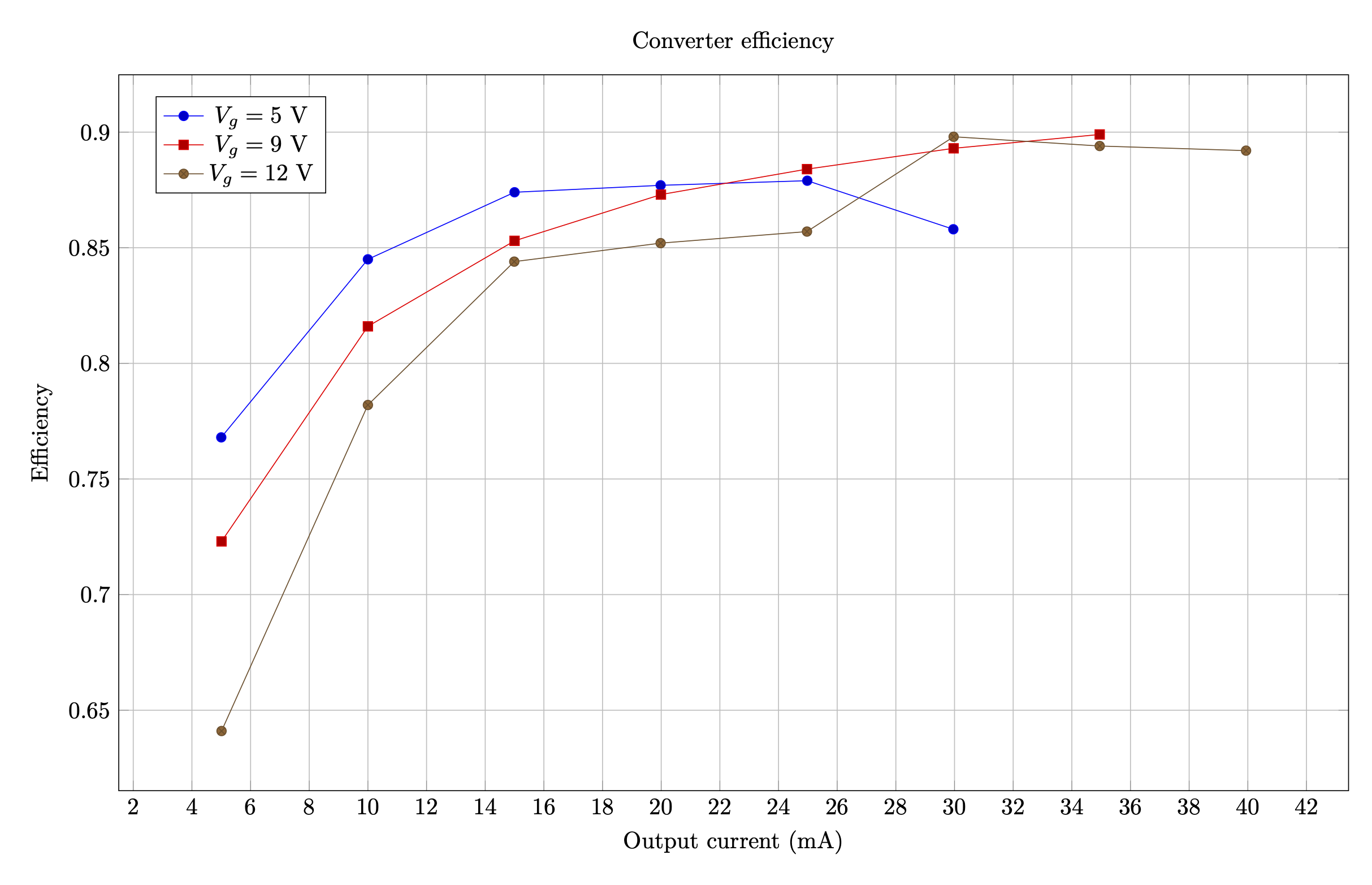
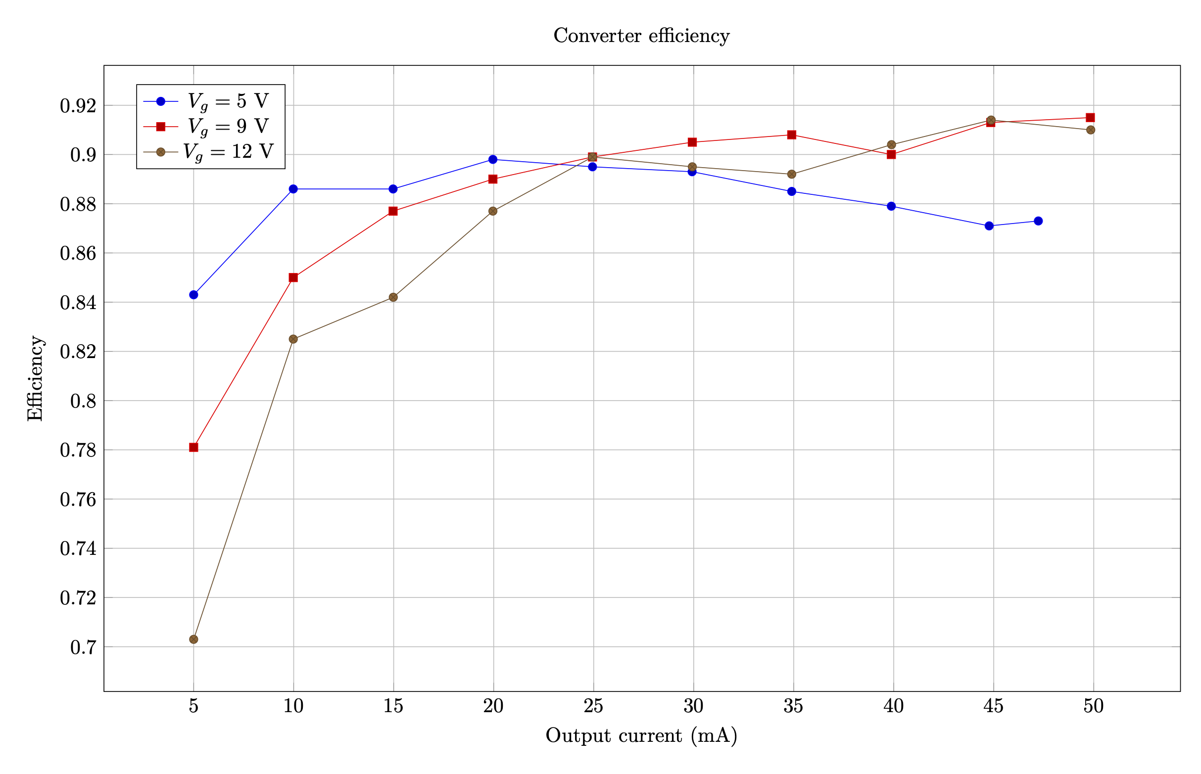
These changes deliver a small hit to the efficiency and limit the output current, but this is to be expected. The converter still achieves about 90% efficiency at high loads at 9V and 12 V input. Efficiency calculation were omitted after the converter hits the current limit.

-
Rev. B evaluations and wrap-up
04/30/2020 at 01:49 • 0 commentsThe rev. B boards arrived and I assembled three of them with the remaining parts. The differences are subtle:
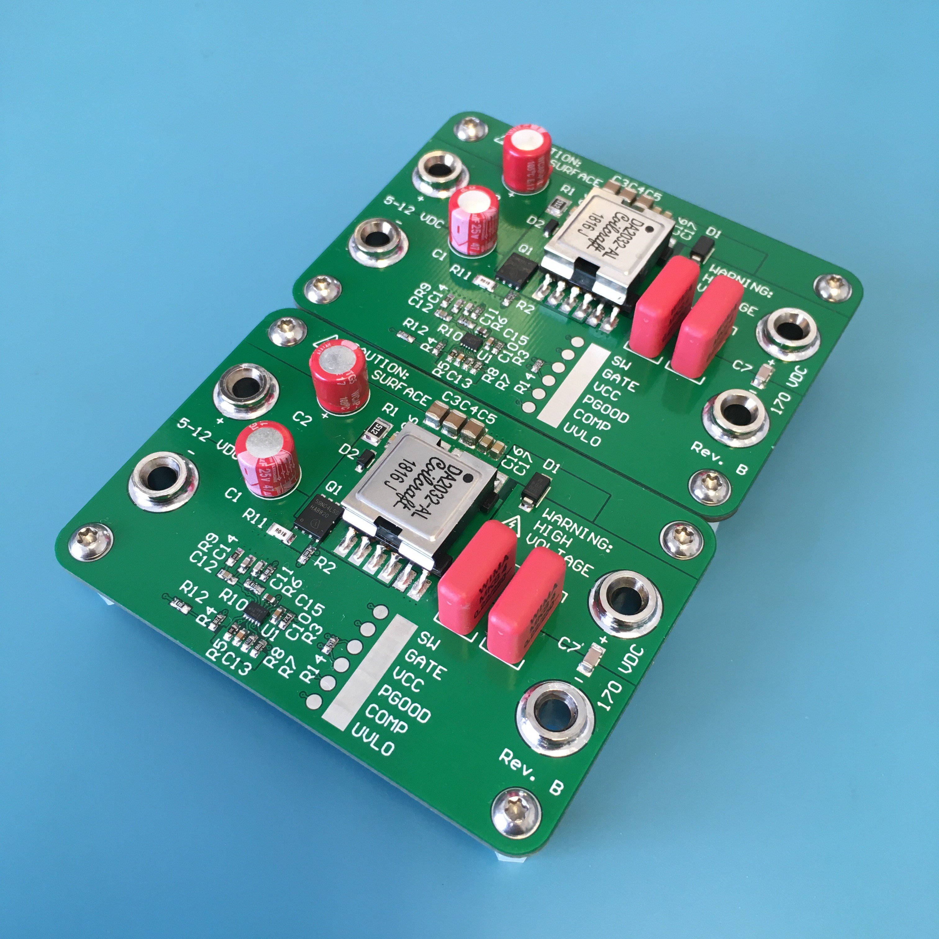
- the input capacitors have been moved adjacent to the transformer, with a clear return path on the bottom side ground pour
- loop gain circuit was scrapped and replaced with a single 20 Ω series resistor for use with an injection transformer
The resulting board is slightly smaller.
Experimental validation of the feedback loop bandwidth
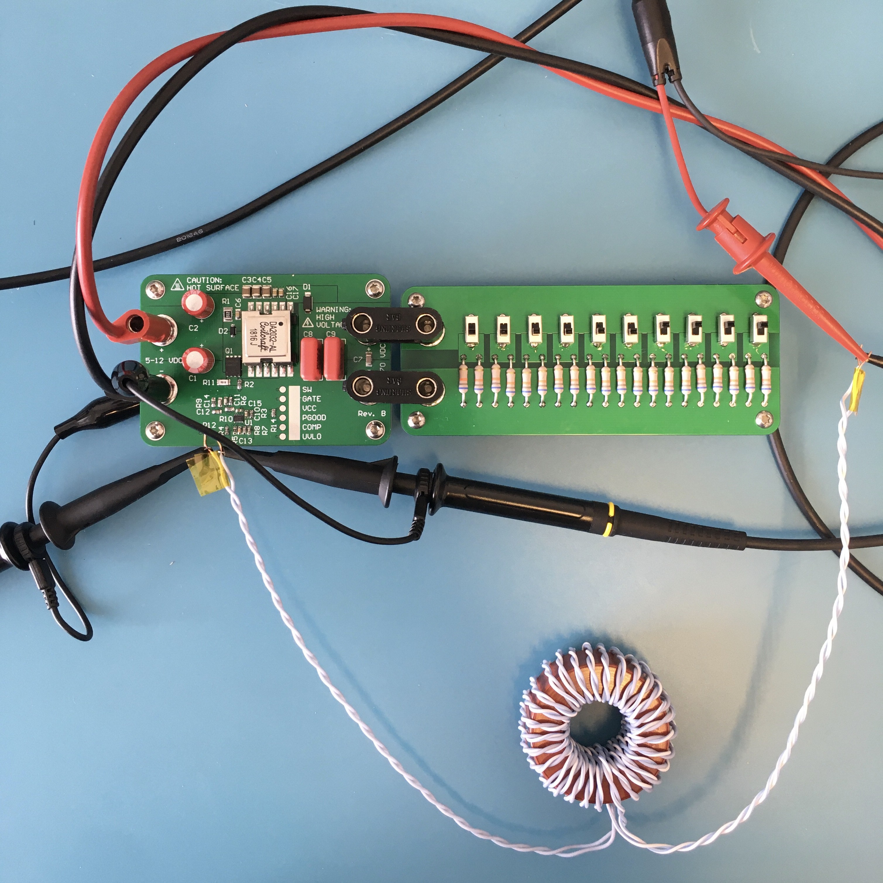
After all the modelling done in a previous section, how good was it? Following the procedure in AN-1889, I connected a 1:1 injection transformer across R12. This transformer is a homebrew device with a bandwidth of 40 Hz - 2 MHz. One side was connected to my scope's built-in function generator, and the other side was soldered across R12. I used the oscilloscope's frequency response analysis tool to produce a Bode chart of the converter's feedback loop.

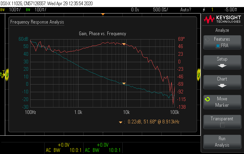
For the original configuration in the design work (fs = 350 kHz, Vin = 5 V, Iout = 30 mA), the measurement shows crossover is at about 9 kHz with a 51° phase margin. The model prediction was crossover at 8 kHz with a 60° phase margin. The shape of the gain and phase curves shows good agreement to the model. If I were going to keep using this configuration, I might tune the compensator's zero frequency to get a little closer to the target phase margin.

For comparison, here is the model prediction:

One of the changes I explored was dropping the switching frequency to improve efficiency. The LM5155 can go as low as 100 kHz, and I made an experiment with fs = 150 kHz earlier, noting that the compensation network might need adjustment. Now that I have the means to measure the loop from a point of relative stability, why not try the practical approach of tuning the components from a real circuit? After the amount of work that went into modelling the CCM transfer function, I'm in no hurry to do a model for DCM if only a minor adjustment is required. The remaining boards run at 100 kHz, so I repeated this experiment at Vin = 5 V, Iout = 30. The results are almost identical.

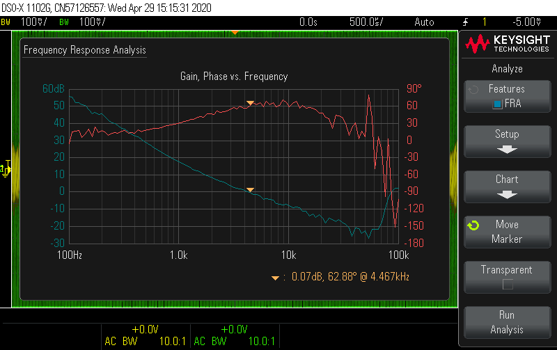
To see how DCM affects the loop dynamics, next I put the converter as deep into DCM as I could by running it at the highest input voltage and lowest current (12 V input and 5 mA output). Here the crossover frequency drops to shy of 5 kHz, with a healthy phase margin.

Before wrapping up this test setup, I also looked at middle-of-the-road configuration: 9 V input, 25 mA output current.

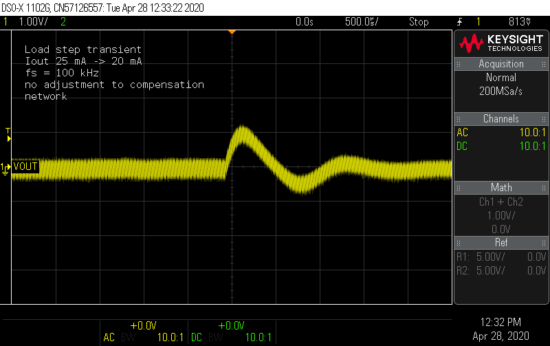
My conclusion is to stick with the current compensation network. Often what happens with DCM is the right-hand plane zero gets kicked out beyond the switching frequency, so using 1/10*fs is a common choice for the crossover, and this shows it's already set close to 10 kHz with a good phase margin. The step load transients (measured on rev A adjusted to 100 kHz) show good response in the time domain as well.


Revisiting voltage ripple and primary snubber
One of the changes was to improve the layout around the input capacitors. For comparison with rev. A, this time I measured the input ripple across the input capacitors, both converters operating at 100 kHz. This shows about half the ripple, with the smaller 1 µF capacitors taming some of the spikes.

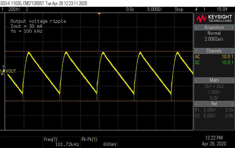
A lower frequency means increased output ripple since I didn't change the output capacitance. At 100 kHz, the voltage ripple increases to 1.4 V (p-p) at full load. This is still less than 1% of the DC level, and Nixie tubes do not need flat DC. Nonetheless, this could still be improved by increasing capacitance, with some possible adjustment required to the feedback loop. In this this package, film capacitors up to 470 nF are available, which would roughly double the output capacitance. For the target application, I'm fine keeping the pair of 220 nF caps.

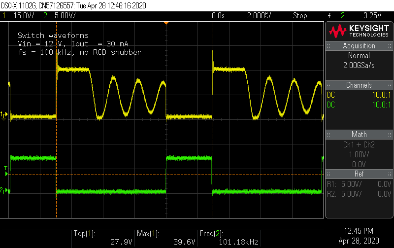
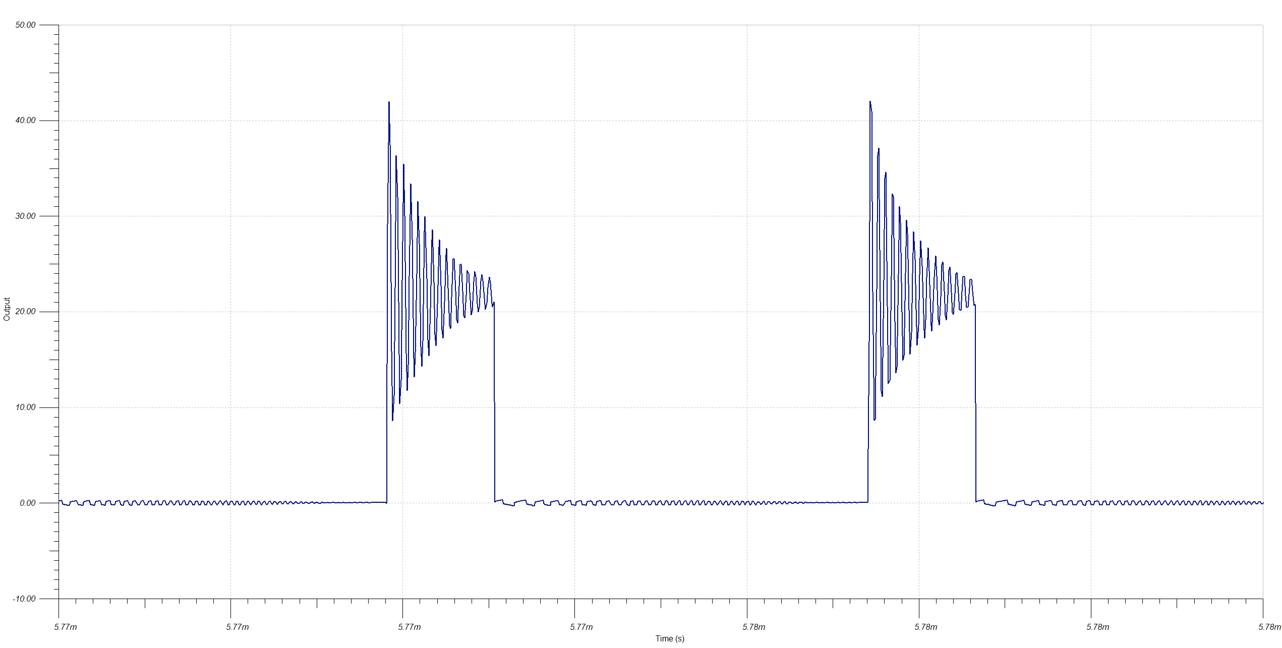
While looking at rev. A modified to run at 100 kHz (with the snubber removed), the switch node voltage saw peaks approaching 40 V, presenting concerns given the Vds rating of the MOSFET.

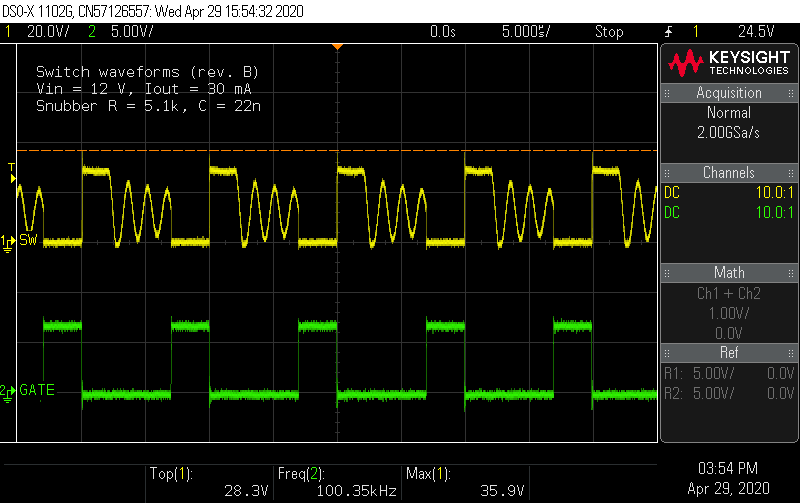
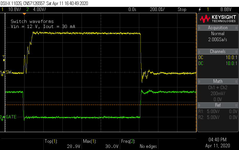
I placed the snubber components for the rev. B boards, and measured the switch node voltage at the highest level configuration (12 V input, 30 mA output). This keeps the switch node voltage at 90% of its rating.

Final efficiency measurements and conclusion
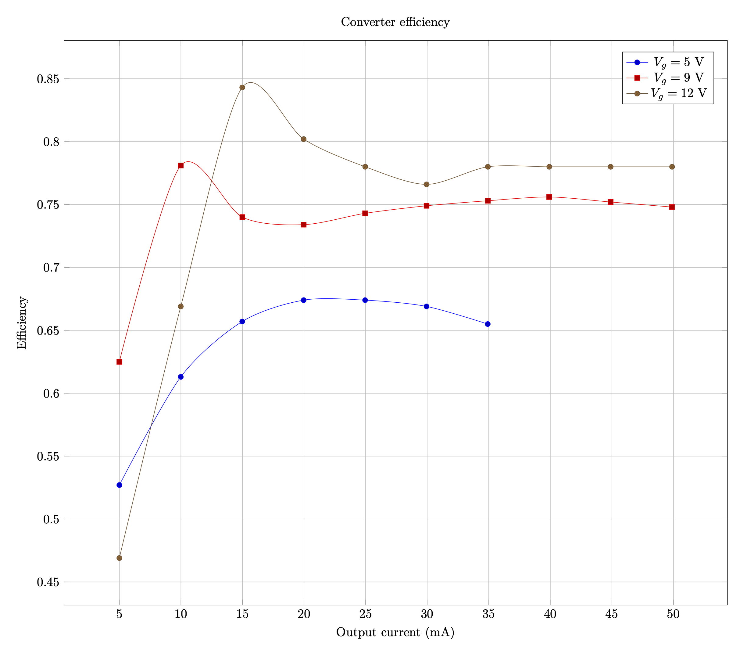
The efficiency measurements at 100 kHz switching frequency show a slight improvement over the previous experiment at 150 kHz. The converter is capable of nearly 90% efficiency over a wide range of conditions, peaking at over 91%. The end of the curve at 5 V shows that current limiting kicks in at Iout = 45 mA, as a precaution against saturating the transformer.

With that, and the end of April arriving, I think it's time to call it a wrap on this project. All of the characteristics of this flyback converter have been verified on the bench. Lastly, just to show it does in fact light Nixie tubes:
-
Going ... discontinuous
04/28/2020 at 04:58 • 0 commentsWhile I'm waiting for the rev B boards, I tried an experiment to reduce the switching frequency to investigate its effect on efficiency. I replaced the timing resistor (R8) with a 150 kΩ resistor, which coincidentally, yields a 150 kHz switching frequency on the LM5155.
At lower switching frequencies, the converter will run in discontinuous conduction mode (DCM), which means the current in the inductor goes to zero in the off state. DCM makes much of the mathematics more difficult, and requires reevaluation of many component choices, but also has some positive effects. I ran the calculations for the current sense network and found the same sense resistor works. One of the consequences of current programmed control in DCM is it is stable without any artificial ramp. Nonetheless, simulation showed the converter is in CCM during startup, so the original slope compensation resistor choice prevents subharmonic oscillations. The compensation network will need changes, but an analytical model of transfer function of the CPM-DCM flyback converter will need some work. For this experiment, simulation showed the existing compensation network is adequate for stability.
I performed the efficiency measurement again, and the results speak for themselves. The lower switching frequency and DCM operation greatly improves performance. The converter achieves peak efficiency over 90% and is in the mid- or high- 80% range across the input voltage range! The transformer remains noticeably cooler, and while the converter hit the current limit at Vg = 5 V and R = 3.4 kΩ (what should have been 50 mA output), it did not show the same thermal runaway.

-
Prepping for rev B
04/24/2020 at 17:31 • 0 commentsWhat worked out well with the initial build:
- Converter maintained voltage regulation well beyond the 30 mA output design limit
- Output ripple was well-controlled
- RCD snubber proved to be unnecessary to protect the MOSFET
- Load transient response demonstrated good loop stability
What was a disappointment:
- The no-break injection circuit didn't work at all and destroyed both the MOSFET and diode on one prototype
- Input voltage ripple shows large spikes
- Efficiency remains close to, but below, 80% under full load
- Thermal problems at high load and low input voltage
Since everyone is still going nowhere, I sent off a second board revision for manufacturing with a couple of changes:
- I removed the no-break injection circuit and replaced it with the more "traditional" way of doing voltage injection by breaking the loop across a small series resistance. This method is documented in TI's AN-1889 and requires a wideband injection transformer. These are a bit of a back-catalog item of test equipment, but it turns out they are eminently homebrew-able with excellent results.
- The ceramic input capacitors have been moved next to the transformer, with a solid ground plane underneath. Additionally, I added a couple of footprints for some 1 µF or smaller capacitors. Throwing additional capacitance in has diminishing returns, but it's easy to leave them unpopulated if they also prove to be of no help. This change also means I can trim 5.5 cm^2 of board space without increasing component density.
The efficiency of the converter could be improved by using a lower switching frequency to reduce switching losses. The choice of switching frequency was driven by the limit I chose on inductor current ripple. Lowering the switching frequency will increase the current ripple and increase the minimum load where the converter begins to operate in DCM. It will also precipitate re-evaluating most of the passive component values, so I'll leave this be for the moment.
-
Parts swapping and efficiency measurements
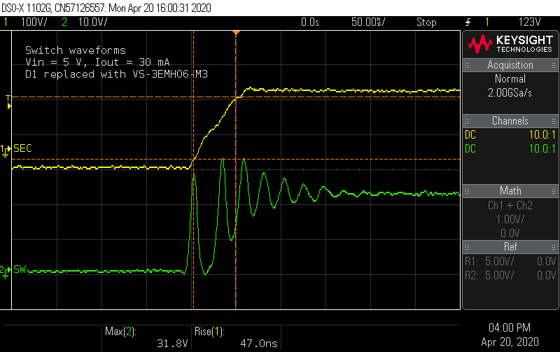
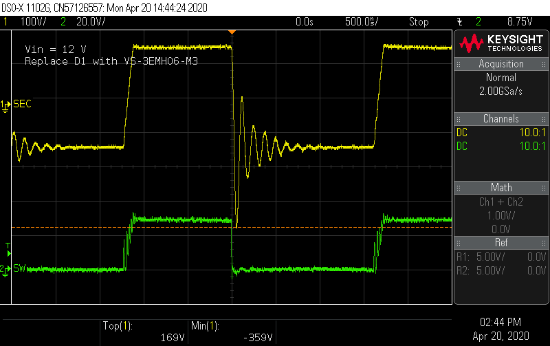
04/21/2020 at 05:19 • 0 commentsI got a shipment with the 600 V-rated ES1J and the VS-3EMH06-M3 diodes. How does a "hyperfast" rectifier compare to the "ultrafast" part I started with? Looking at the voltage on the rise time on the secondary shows it's close to twice as fast (47 ns vs. 90 ns). Already it appears the switch node ringing is starting at a higher amplitude.
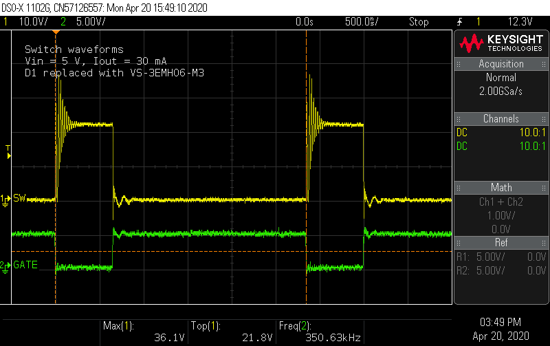
 Probing the switch node shows a ringing waveform that looks much closer to the simulation. At the maximum inductor current condition, the voltage spikes are still 10% below the MOSFET Vds limit, without any snubber.
Lastly, the reverse recovery situation looks about the same, with the reverse voltage spiking to 530 V.

Overall, it seems this new diode is nothing special by comparison, but the 600 V rating is important given the voltage ringing during reverse recovery.
Efficiency measurements
I waited to make efficiency measurements because I wanted to settle on a configuration to use after considering options for the snubbers or other adjustments. For this test, the measurements were taken with the VS-3EMH06-M3, and without RCD snubber network. I used the source display on my bench power supply to read the input power, and measured the voltage at the converter's output terminals and the current between the converter and load board. Of course, it'd be nice to do all this with ATE that would gather the data while I made on some coffee, instead of by hand ... perhaps someday.


At 9 and 12 V, the converter is about 75-80% efficient, with a sweet spot around 15-20 mA where it peaks over 80% with 12 V input. It would have nice to be consistently above 80%, but it appears core losses in the transformer are the limiting factor. It is easily the warmest component on the board during operation.
I didn't take measurements at 5 V beyond 35 mA, because at high load, the current in the transformer is high enough that causes a thermal runaway. Heat increases resistance and voltage drop, so the converter adjusts by increasing duty cycle and average current, which further increases heat. Eventually the converter hits the current limit or the transformer core begins to saturate. At the 5 V, the converter should be thermally derated to 25 mA maximum current to keep the transformer from overheating, unless active cooling is done.
The last parts experiment I had was to test polypropylene (PP) output capacitors. PP is supposed to have lower dissipation factor by an order of magnitude compared to polyethylene terephthalate (PET), so it should handle pulse currents better. Would it help improve efficiency beyond the 75-80% level? I replaced the output caps and reran the efficiency experiment. The result was basically a wash. A few fraction of percentage points here, a few there. No data point changed by more than 1 %, which doesn't justify their added cost.
-
More evaluations
04/19/2020 at 22:20 • 0 commentsThe previous update looked at voltage ripple and transients. Another important area to investigate is the switching waveforms. This shows the switch node and gate voltages.
 ---------- more ----------
And a close up:

The first thing to notice is that the ringing predicted by the simulation is almost nowhere as bad. Instead of rising and overshooting the off-state voltage of 22 V, it's taking a while to reach that level while ringing on the way up. This happens regardless of input voltage:


What's going on here? The snubber was expected to clamp the switch node voltage to 32 V, but the voltage never gets close. Before investigating further, it's worth commenting on the gate waveform. I added a 0 Ω series jumper in the design as an option to damp any ringing at the gate. The BSC059N04LS6 datasheets puts the Vgs(th) figure at 2.3 V max, so even at 5 V input, the switch is squarely on, and it seems the waveform is clean enough not to require additional series resistance at the gate.
Back to the weird rising waveform at the switch node. Probing the secondary side reveals a clue.

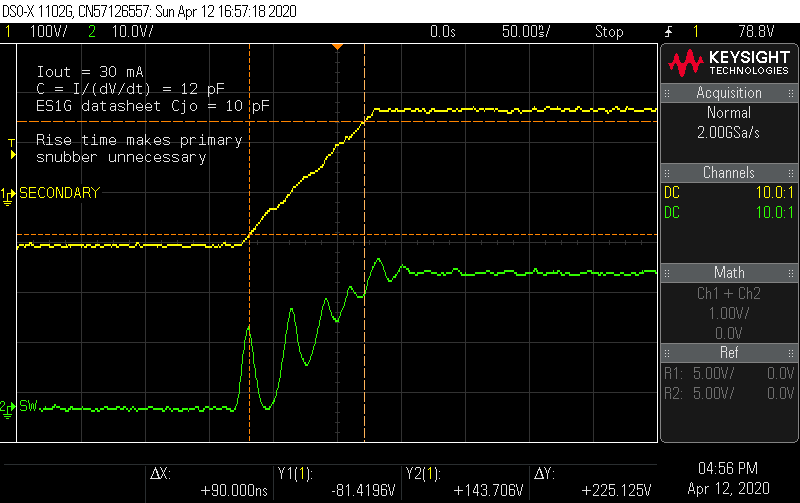
The secondary voltage ramps as if a current source is charging a capacitor, which happens to be the real junction capacitance of the diode, closely matching the datasheet value. The ringing at the switch node has to follow this voltage ramp, so the ringing starts from a lower amplitude and decays before the switch node voltage reaches the full off-state value. Here is the first big departure from the simulation: it appears the diode model for the ES1G doesn't accurately model the junction capacitance. When I re-ran the simulation, it predicted a diode rise time of less than 25 ns.
As a side-effect, the primary side RCD snubber is not really helping anything. The voltage across the snubber capacitor remains about 16 - 17 V, so I removed it and found no change in power consumption.
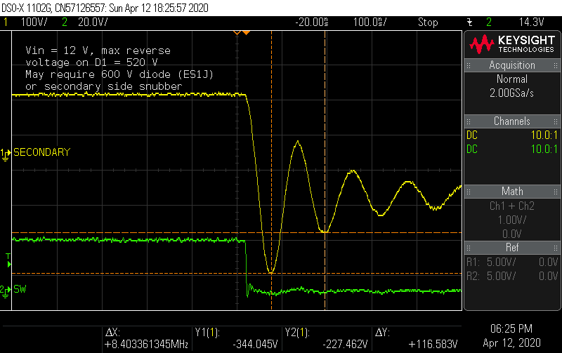
The simulation also predicts an oscillation at the secondary when the diode turns off, which is confirmed on the oscilloscope.

With the other side of the diode at 170 V, the diode sees reverse bias spikes of nearly 520 V. This ES1G diode has a VRRM (maximum repetitive reverse voltage) of 400 V, so this ringing is probably going to reduce the service life of this diode. There are a few options to correct this situation: place a higher-rated diode (such as the 600 V ES1J), add a snubber across the diode, or try a different diode with better reverse recovery characteristics.
How much will a snubber help, and what will it cost? To experiment with a snubber, I first measured the frequency of the oscillation. The resonance exists between the transformer's leakage inductance as seen on the secondary side, and the parasitic capacitance of the diode junction as it goes through reverse recovery.
 The primary side leakage inductance of the DA2032 is 150 nH, so it will n^2 * 150 nH or 15 µH on the secondary side. At an oscillation frequency of 8.4 MHz, the capacitance for this resonance is 24 pF, and the characteristic impedance (sqrt(L/C)) is 792 Ω. An RC snubber design trial should start with this resistance and a capacitance of 4 - 10x the parasitic capacitance.
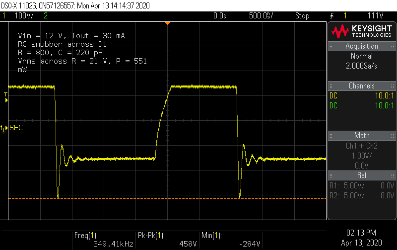
I have some assorted 250 V 0603 caps in the 100-1000 pF range, so I bodged on two in series to withstand 500 V. A 0603 820 Ω resistor exploded instantly. A single 1/4 W through-hole resistor also started smoking with a second. Substantial power was being burned off in this snubber. Finally I tried a fixture of four 1/4 W 3.2 kΩ resistors soldered in parallel, and even then, the paint on the resistors began to discolor within a few minutes. This wasn't looking promising, but I took some measurements nonetheless.

The snubber has reduced the reverse bias spike to under 460 V, but at a dear cost. Measuring the AC voltage across the resistor network showed it was dissipating over 1/2 W. That's going to wreck the efficiency of the converter, and for what? A higher-rated diode is still needed.
Dissapointed, I removed the bodged-on snubber, and ordered a few pieces of the ES1J and another diode I found, the VS-3EMH06. This diode is a "hyper-fast" rectifier (evidently the ranking is standard, fast, ultra-fast, super-fast, hyper-fast ... real helpful) with also a "soft recovery", so I'm curious to see how it will perform. There are even faster diodes out there in this lineup, but they are rated for higher current, are more expensive, and use a larger footprint. There are not a great many diodes that are designed for modest forward current, high reverse voltage, and highest speed. I'll see how this diode performs in the next update.
-
First evaluations
04/19/2020 at 19:47 • 0 commentsThe boards were produced by JLCPCB and in my hands within a week, very nice considering concerns about the global economy at the moment. I assembled identical boards, one as a reference and the other to be poked and probed, and sacrificed if needed.
 ---------- more ----------
Load board
I don't have an electronic load, which makes testing power supplies a lot easier. Even if I did, most general purpose e-loads aren't set up well for the corner case of high-voltage, low-current power. Even though this board sources less than 10 W, I'd need an overspecced e-load just to handle the voltage rating, or use something like an SMU (even more expensive).
So along with this board, I also had a second board made that lets me adjust the load manually in steps. Each switch on this board adds a branch with two 1 W 68 kΩ resistors in parallel, or 34 kΩ. 170 V into 34 kΩ gives 5 mA per switch, so the output current can be stepped from 0 - 50 mA.

Startup transient
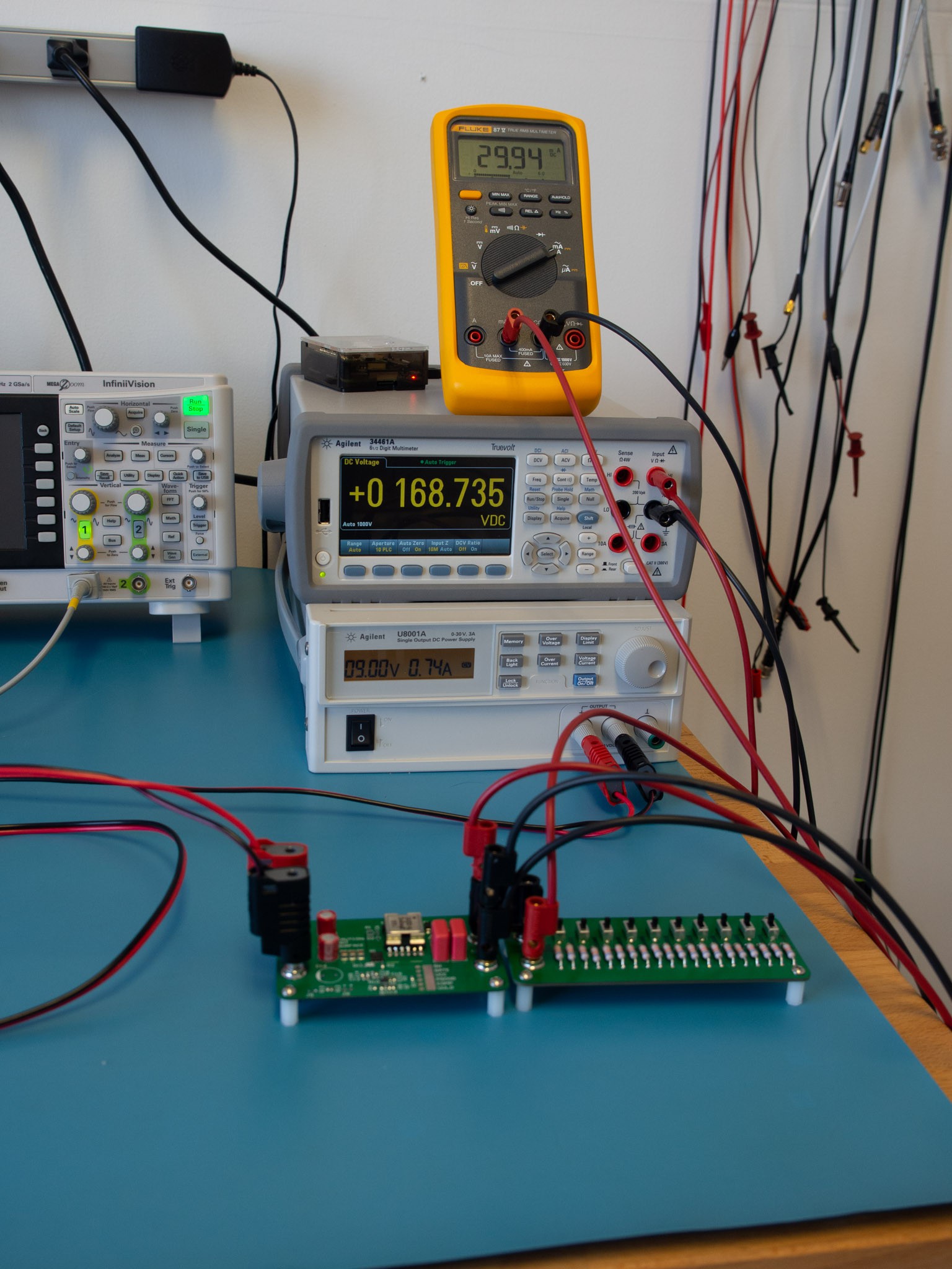
Does it work? Connecting the inputs to a bench supply the and output to a multimeter, I anxiously flipped the switch, and heard ... the satisfying click of my multimeter's autoranging relay followed by a reading of 169 V! Connecting the load board, I flipped the switches and watched the voltage remain rock-steady as I pushed the load current to 50 mA. Satisfied that nothing was going to give off smoke, I started characterizing the board on an oscilloscope.
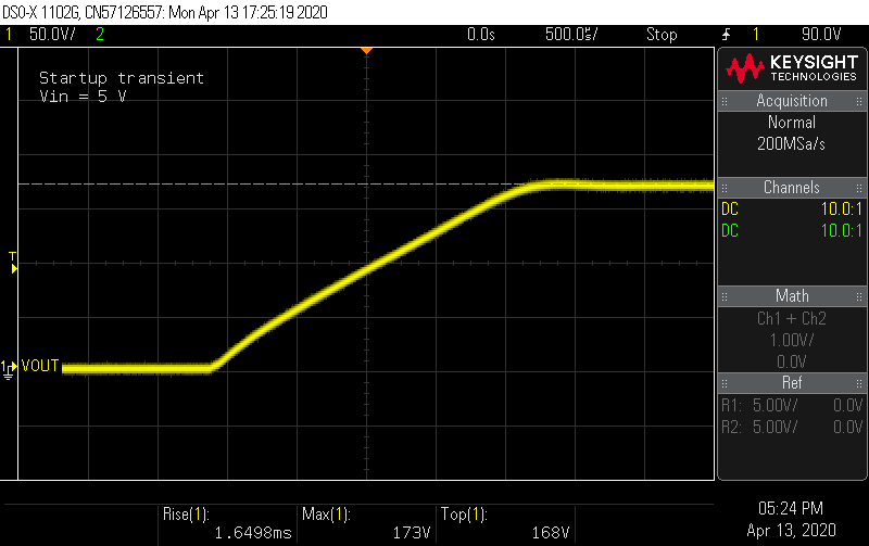
Setting a long time base, I examined the startup ramp transient. At 5 V and 12 V input voltage, it looked identical.


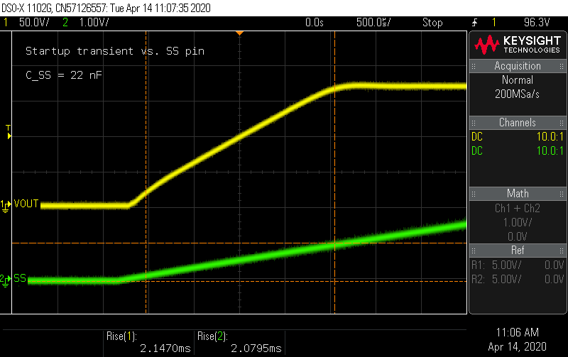
The startup time seems fixed. Well, there was that soft-start feature... The soft-start ramps up the feedback control voltage as the soft-start capacitor charges to 1 V. How does the SS pin voltage and ramp time compare to the output voltage? I set the rise time measurement on the output voltage to measure 0 to 100% (usually rise time is cited as 10 - 90%) and an absolute rise time for the other channel with a limit of 1 V.

10 µA into 22 nF rises to 1 V in 2.2 ms, so that looks right. What happens if I replace C_SS with something larger, like an extra 68 nF from the compensator circuit? I'd expect the rise time to go to 6.8 ms...

Bingo! I kind of like this a bit more. The slower rise time appears to eliminate the mild voltage overshoot that's noticeable with the original 22 nF choice.
Load transient
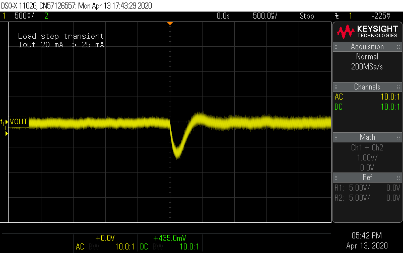
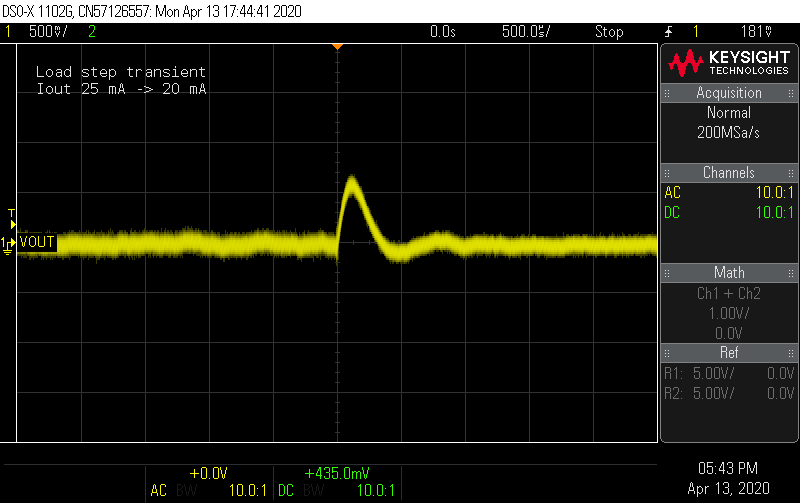
Next, how well does the controller handle a sudden change in load? In the simulation, I used a 15 mA load step, but try as I could, there's no way to flip 3 switches at exactly the same instant, so I only captured the step load transient for a 5 mA step. These are AC-coupled captures, so going to zero means a return to regulation.


In the design phase, I used a crude estimate of the converter's output impedance to size the output capacitance to limit the load transient to 1 V at a 15 mA load step. In simulation, the result looked closer to 2 - 3 V. Here the transient is about 700 mV for a third the size of the load step, so that the simulation looks like it's predicting things well.
Another way to understand the load transient is look at the feedback loop response. I added a circuit to permit injecting a function generator signal into the feedback loop. Unfortunately, it didn't work as planned. Once the jumper to ground is closed, the large capacitor (1000 µF) pulls down the FB line voltage causing the output voltage to spike. This stresses all the components and destroyed one of the test boards very quickly. The board can't withstand the high voltage during the charging time, even if the coupling capacitor is reduced to 100 µF. It's disappointing this part doesn't work after all the theoretical work that went into designing the compensation network. There are other ways to make measurements of the loop gain, but they involve breaking the feedback loop and will require a board respin. Wary of destroying my remaining board by a careless short of one of those headers, I removed those components for my remaining tests.
Output ripple
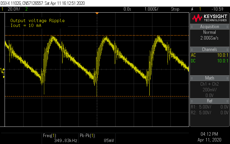
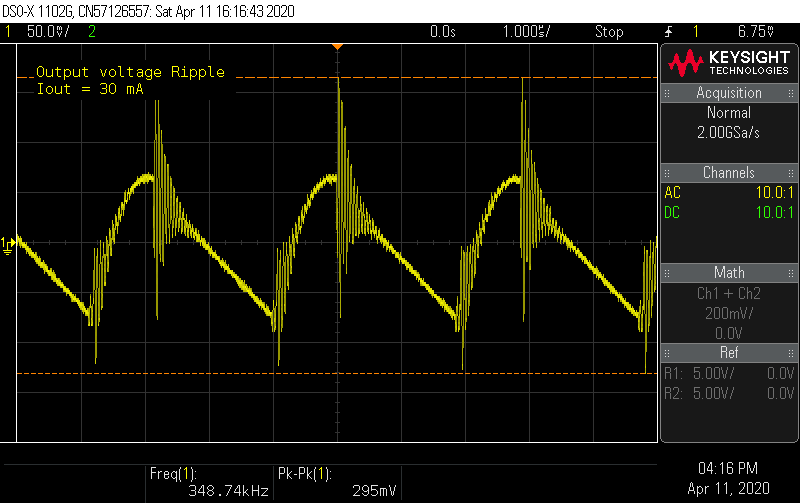
Output ripple measurements were made by probing directly across C7 in AC coupling mode. There's definitely some high frequency component that's modulated with the lower frequency ramp up and down.

At 30 mA load, these spikes get larger, but overall the ripple is manageable at less than 300 mA. From the output ripple formula, at 30 mA, the output ripple should be about 150 mV, which if you ignore the ringing not predicted by the formula, looks about right on.

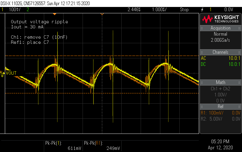
Is the 10 nF capacitor C7 doing anything? Should it get to keep its job? Let's remove it and see what happens.

Seems the 10 nF ceramic capacitor really does help after all.
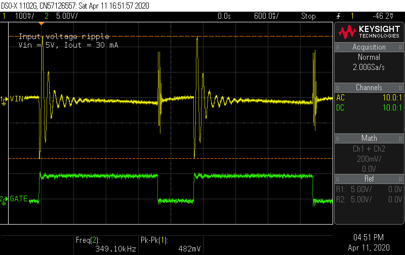
Input ripple
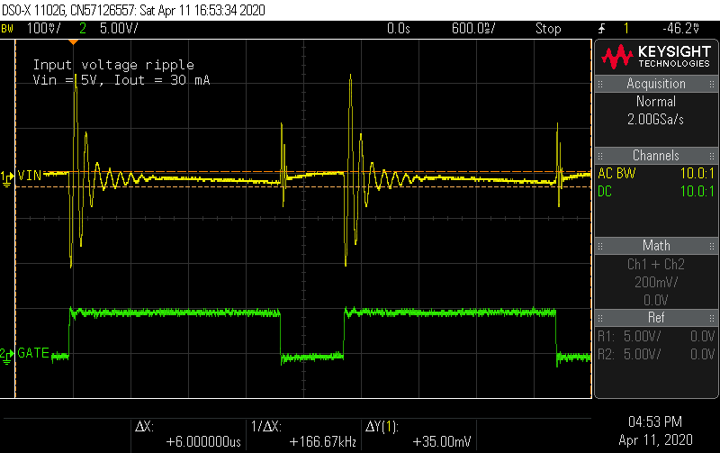
Probing directly across the input terminals, I measured the input ripple. There are ringing waveforms at the edges of the switching cycle, but the low frequency ramp appears to have a peak-to-peak amplitude of about 35 mV, which was close to the design target.


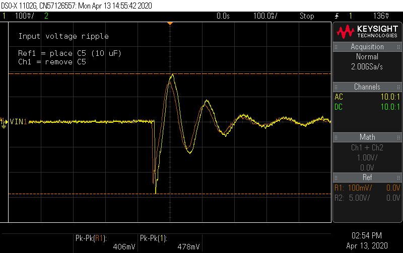
What effect do the three ceramic caps C3, C4, and C5 have? Removing the last one shows some mild effect.

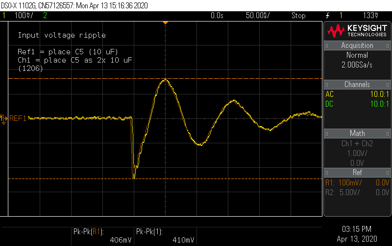
I squeezed two 1206 10 µF caps into the space of one 1210 and measured the result. It appears the point of diminishing returns has been reached.

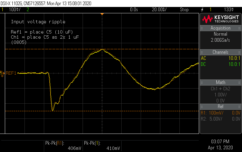
What about additional capacitance in a lower decade? I tried the same trick with some 1 µF 0805 caps.

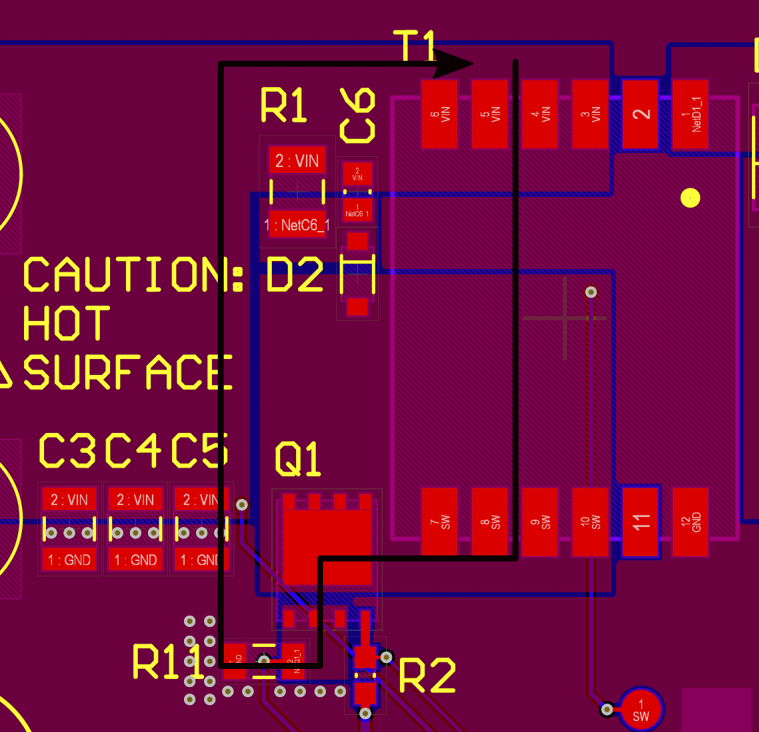
Unfortunately, it appears additional capacitance cannot reduce the spikes at the input. The more I looked at things, the more I suspect that a poor layout choice might be responsible. When the switch turns on, the source current instantly jumps to the average inductor current. Small capacitors will be the lowest impedance path for a sharp current step, so the current will prefer to go through the bank of ceramic capacitors. Under load, the inductor current is substantial and any stray inductance in this loop will cause sharp voltage spikes. Inductance is related to loop size, and the placement of the capacitors forces a sizeable loop on the top layer. Current can also flow on the bottom layer under the path from T1-Q1-R11, around the trace that cuts the ground plane, and then double back to reach C3-C5. It's hard to guess what is the actual lower inductance path.

A better layout would be to move C3, C4, and C5 directly adjacent to the transformer pads and let the current flow underneath the path on the bottom layer, which greatly reduces the loop size. This too will require a board respin.

-
Prototype layout
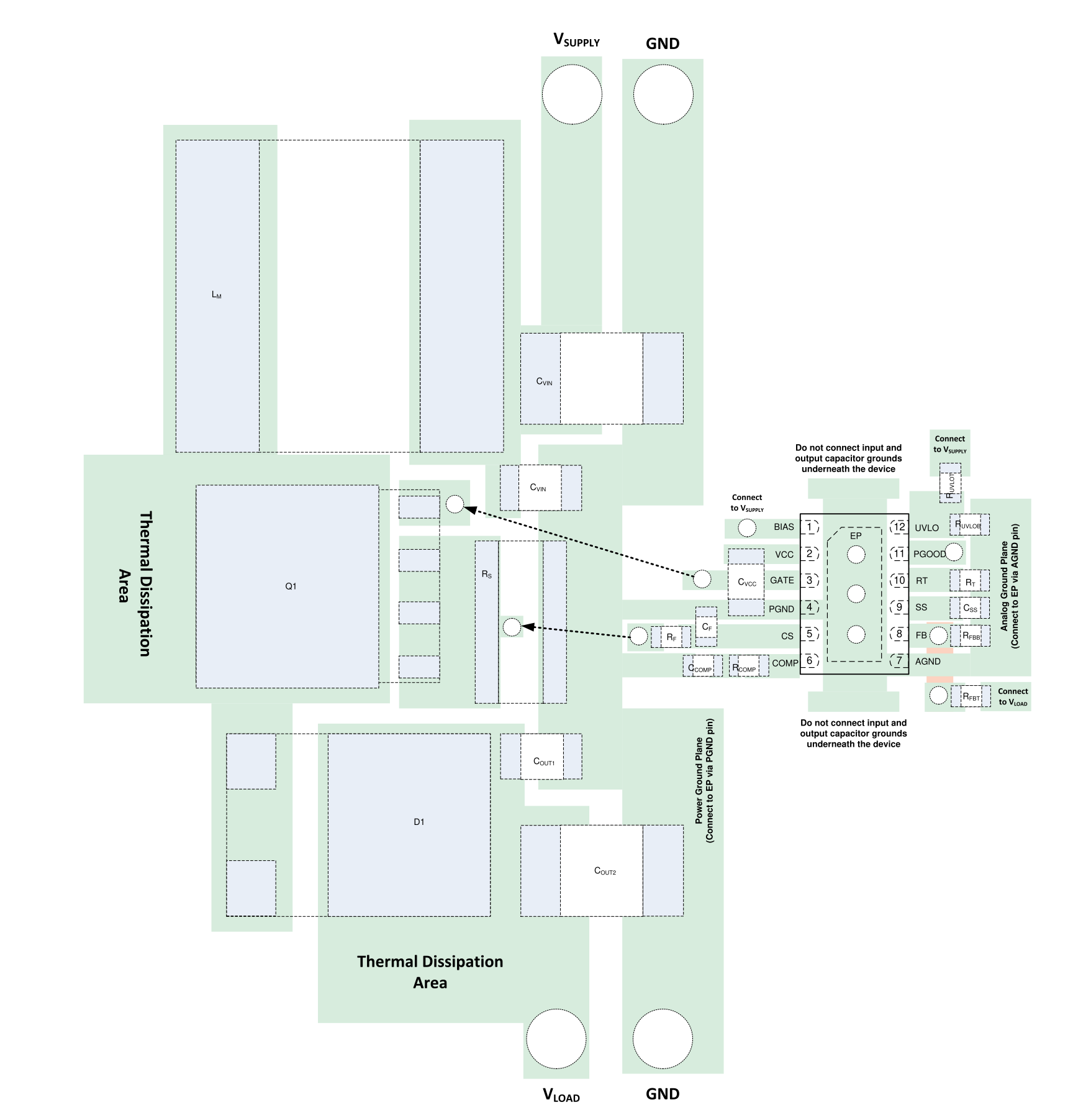
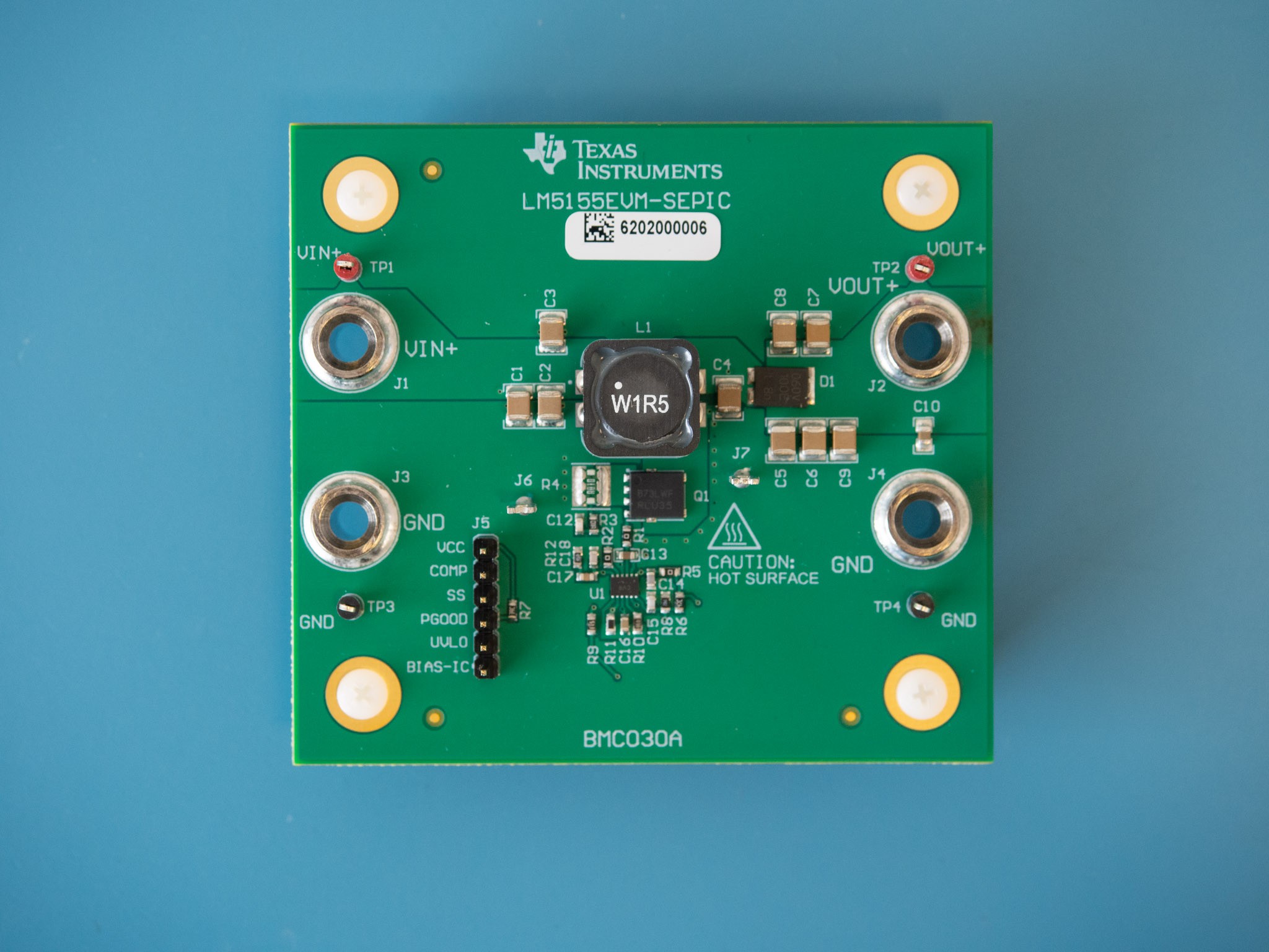
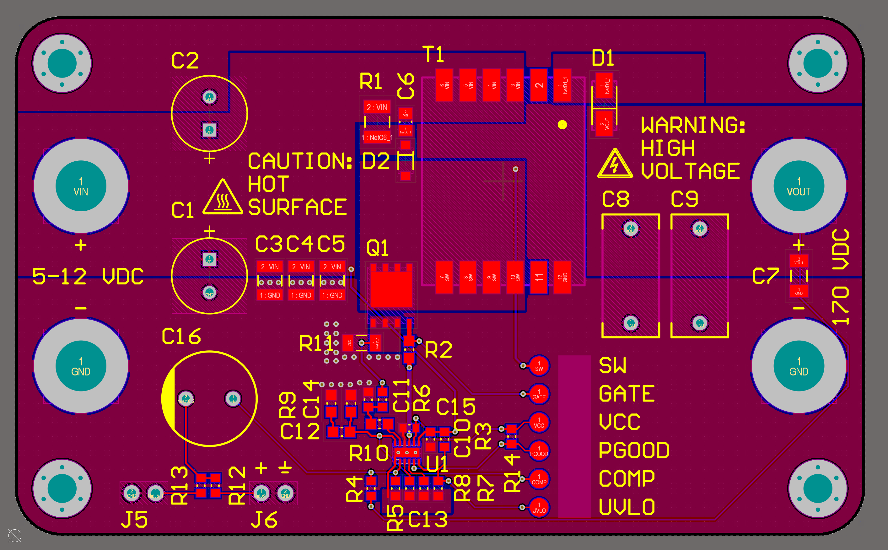
04/18/2020 at 23:29 • 0 commentsFor this project, I wanted to justify all component values from first principles. On the other hand, for PCB layout of a SMPS, I'm more than happy to copy a layout that works. In this regard, the datasheet for the LM5155 provides very helpful layout guidelines and examples, and the engineering team at TI also produced three evaluation boards (in boost, isolated flyback, and SEPIC topologies) that also demonstrate good layout.
---------- more ----------

For my test board, I wanted to follow in the "evaluation board style", which to me means:
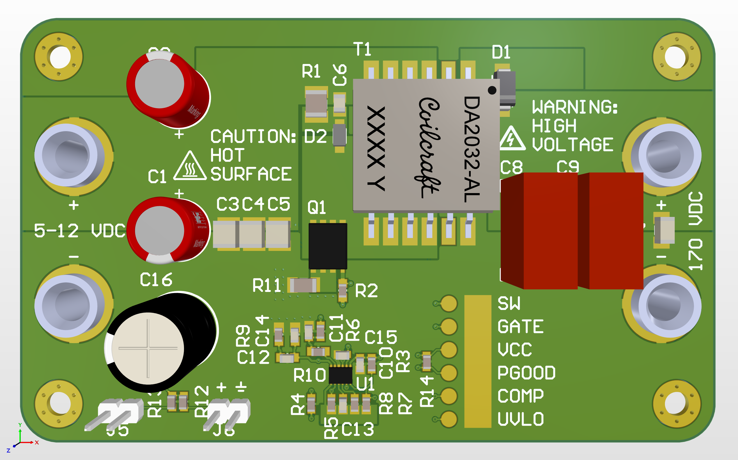
- Medium- to low-density design where there's plenty of room to probe and rework parts. Anything that I think I might tune, I use low-density footprints and leave space to rework the area and bodge on parts.
- Prefer larger component packages that are easier to rework, no smaller than 0603 for passives.
- Lots of test points. Commercial boards often use soldered-on loops for test points, but these get expensive in quantity, and an exposed pad with a nearby ground point works just as well.
- Power terminals accept big banana plugs for fast, positive connections to meters and power supplies.
- Screw holes and standoffs at the corners make it easy to keep the board stationary while attaching probes.
As the flyback power stage is the only thing on the board, routing should be uncomplicated, and I used a 2-layer layout like the examples and commerical evaluation boards.

 Next step: send for manufacturing, assemble & test!
 -
Simulation
04/18/2020 at 19:48 • 0 commentsWith components selected, it's time to move toward realizing this converter. The next step will be testing the design in a circuit simulator.
People like to gripe about LTspice's outdated UI, but I've gotten pretty fast at sketching up circuits with it. Unfortunately, the LM5155 SPICE model is encrypted and only works in TI's SPICE variant, TINA-TI. TINA-TI is free to download and use, but LTspice is in many ways leagues better. Want to peek at some node voltage? In LTspice, just click on the node in the schematic after the simulation is done. In TINA-TI, the transient simulation only records voltages and currents for explicitly added meters, so that means adding a meter and re-running the simulation.
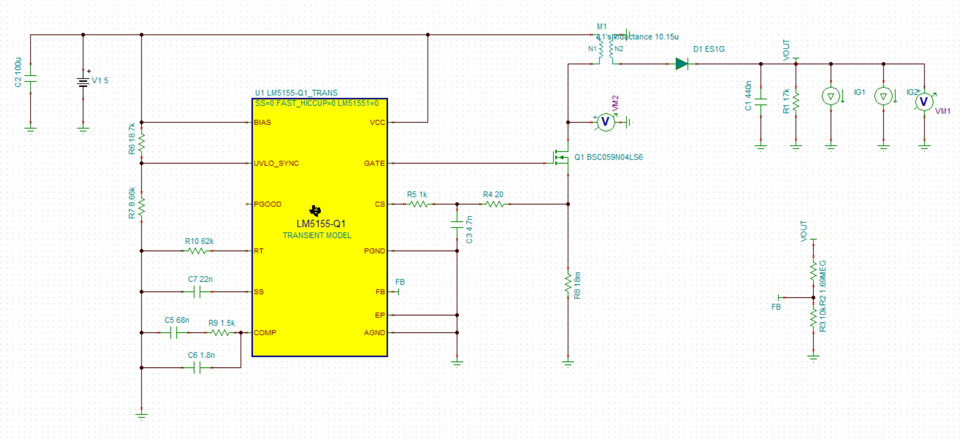
---------- more ----------Here's the converter schematic in TINA-TI:
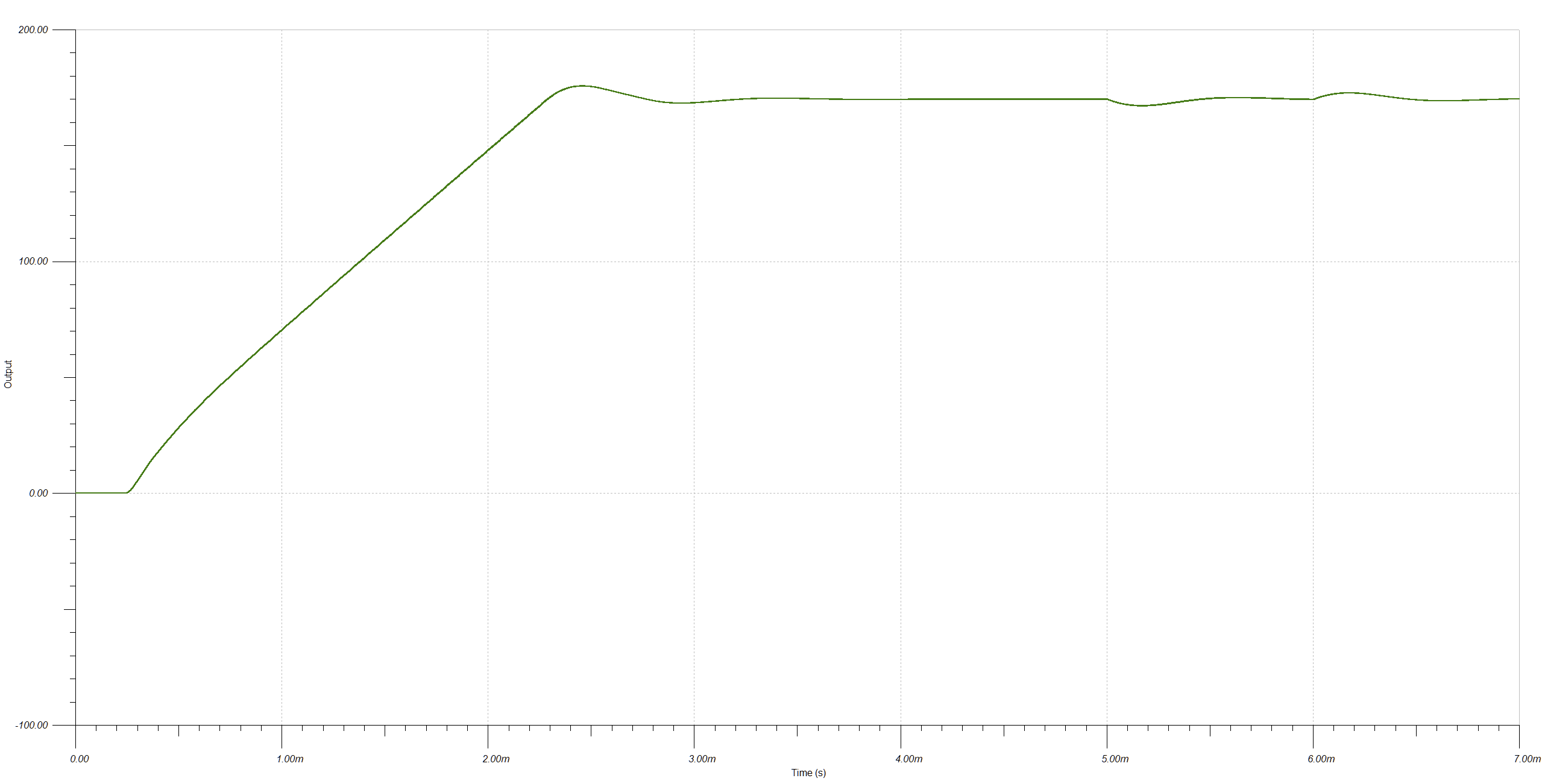
 I changed the initial load to 11.33k to get a 15 mA output current and added time-delayed step current sources IG1 and IG2 to simulate a load step-up and step-down of 15 mA. Here's the output voltage plot, showing the startup ramp and load step at 5 ms/6 ms:
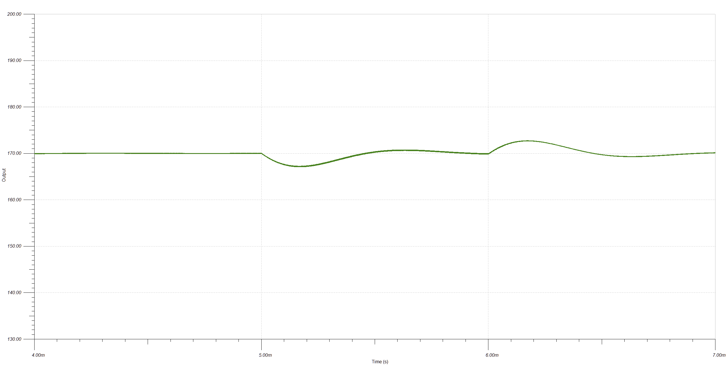
 Close-up of the load step transient shows the transient is larger than 1 V as predicted by formula used to pick the output capacitance, but it seems acceptable for the application. The converter returns to regulation within a millisecond and shows good stability.
 Looking at the switch node or MOSFET drain at full load, there's a problem: the voltage is spiking above 40 V and will need a snubber.
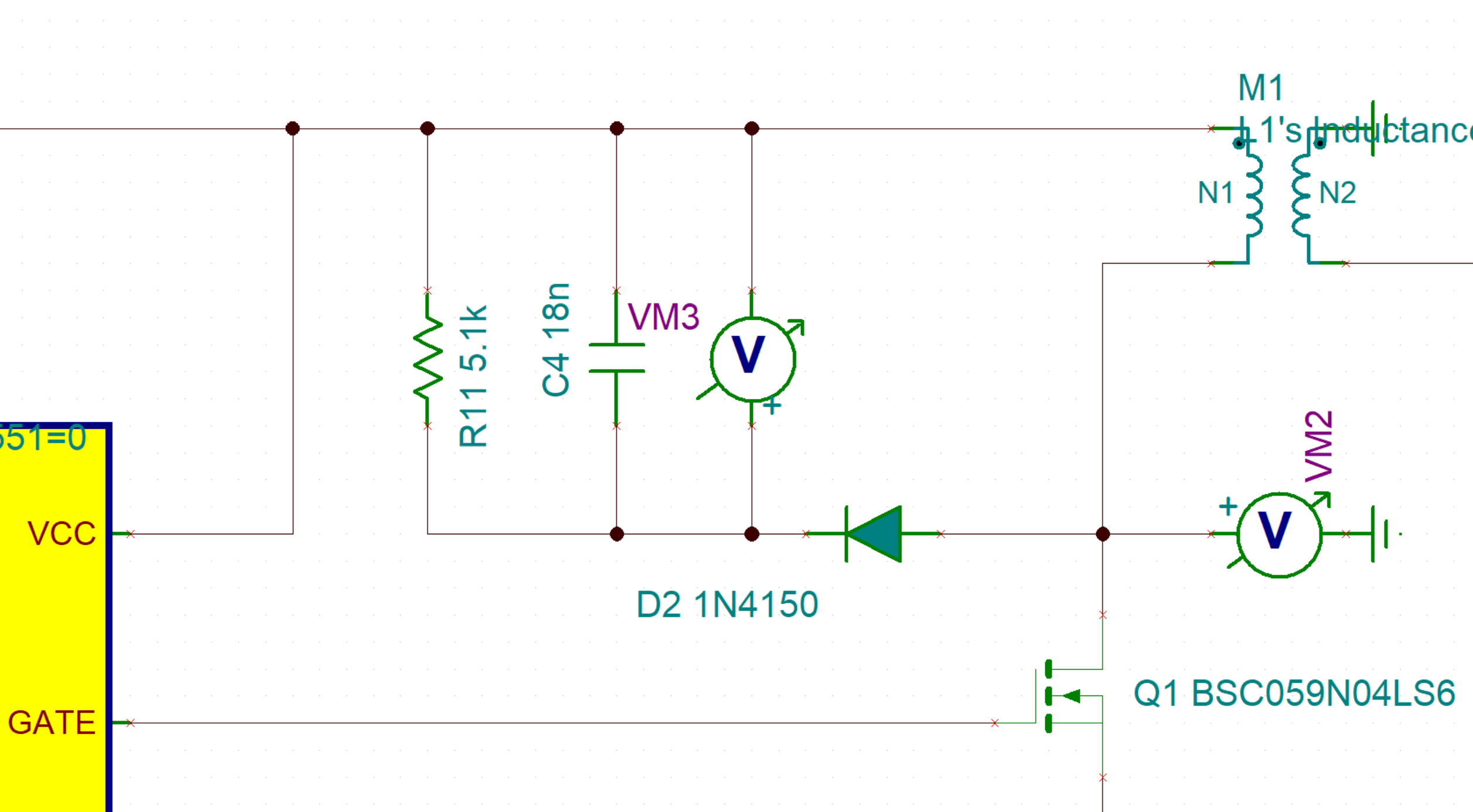
To build the snubber circuit, I turned to application note from Fairchild Semiconductor, AN 4147, that describes how to design a RCD snubber for a flyback converter. Even though it has "RC" in the name, the RCD snubber is nothing like a RC snubber that tries to damp resonance through matching the characteristic impedance of the parasitic elements. I spent a lot of time trying to understand this circuit before I realized it's actually similar to a boost converter that's driven by the resonance between the leakage inductance and MOSFET output capacitance, instead of a PWM gate driver, making it a kind of resonant converter! In this case, I selected a snubber voltage of 32 V or 80% of the MOSFET's rating, and the design equations in AN 4147 yielded R = 5.1 kΩ and C = 18 nF. I picked 1N4150 as the diode, it's rated to 50 or 75 V depending on the particular manufacturer, and is quite fast. This is the snubber circuit added in the simulation:
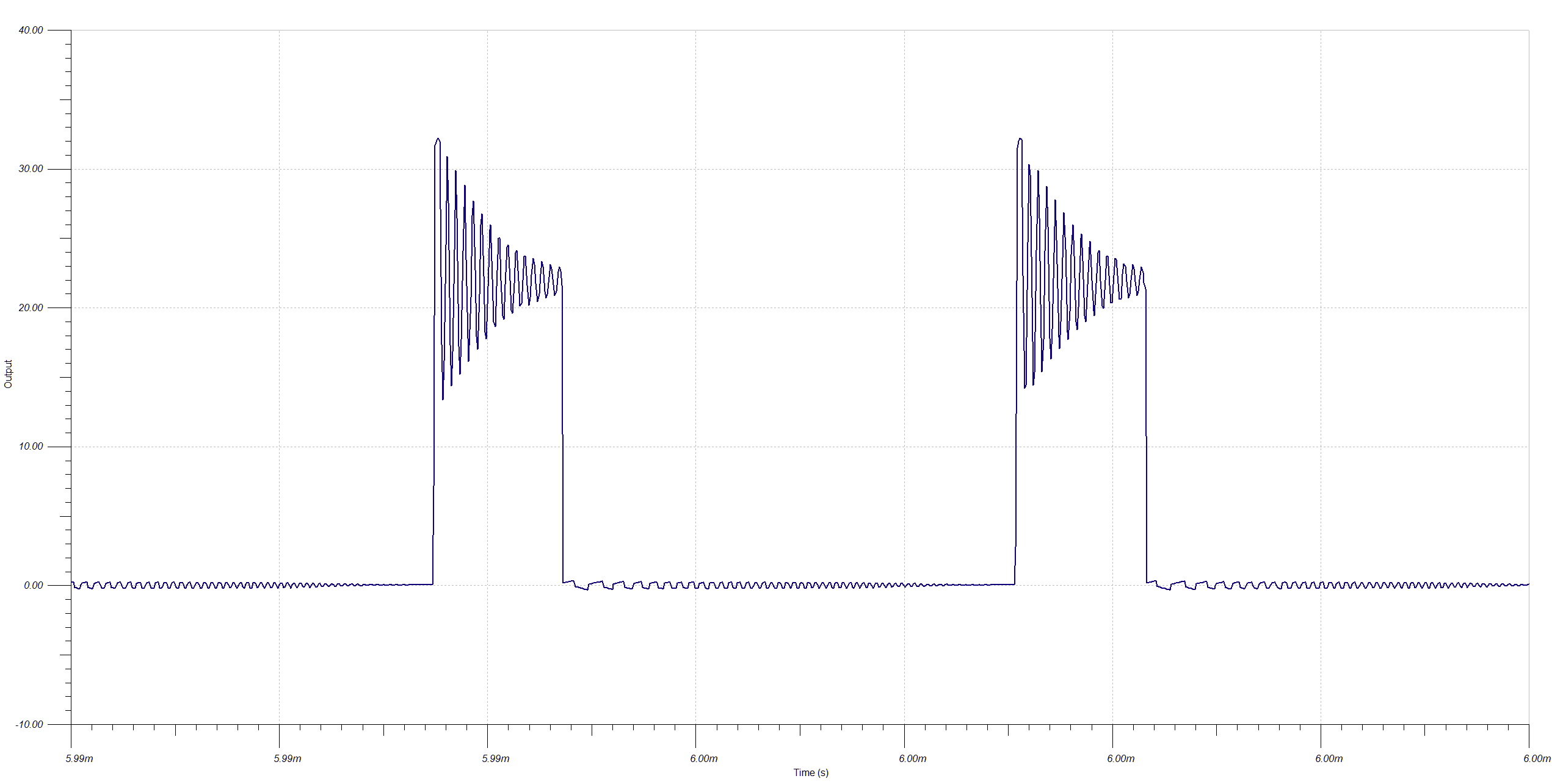
 The simulation with this circuit added shows the switch node voltage gets clamped at 32 V as predicted. There's still a lot of ringing, but the goal of protecting the MOSFET has been achieved. Snubbers always need experimental verification and tuning, but this looks like a promising starting point.
-
Closing the feedback loop
04/18/2020 at 02:21 • 0 commentsA converter needs a feedback mechanism to maintain voltage regulation. The choice of a duty cycle only works for a particular set of load resistance and input voltage. Variations, large and small, need to be corrected to maintain a stable output voltage level. Feedback loops are fickle things, and unless carefully constructed, can become unstable. Stabilizing the feedback loop is the purpose of the compensation components attached to the controller chip.
There are few ways to determine how to compensate the loop, generally it's either relying on some intuition (or cribbing from something known to work) and then experimentally verifying it, or it's deriving an analytical model of the converter's feedback loop and solving for the optimal component values. I'm going to try to do the latter in this log. Unfortunately, the derivation alone can take pages, even with a background in control theory, so I'm unsure how much to document. I can always add detail on request.
The LM5155 control loop
This is a simplified view of the control loop of the LM5155. The "hat" notation refers to small-signal variation, i.e. a linearized model of how the system behaves when values are perturbed from their normal DC operating point.
---------- more ----------
Starting on the right, the output voltage is passed through the sensor block H. This is just a resistor divider with a gain of 1/170 for this converter. This is subtracted from the LM5155 voltage reference, creating an error signal. The error signal is fed through the compensation network, and then voltage is converted to a current value by the resistance of the sense resistor. The resulting current control signal is fed into the current programmed controller and the current-to-output gain Gvc determines the feedback output voltage. Determining the structure of Gvc (all its poles and zeros) is the hard work of the analytical path.
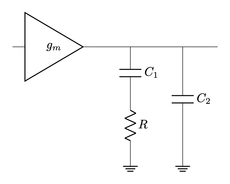
Current mode controllers generally need a simple compensation network, called a type II compensator, that is just a shunt resistor and capacitor in series. This has an origin pole and a zero at the RC corner frequency. An optional high frequency pole is added by putting another capacitor in parallel with the series branch.

To determine Gvc, the first step is derive a small-signal AC model of the converter. This can be obtained through my preferred method of state-space averaging, or by circuit analysis using an averaged switch model.

From the small signal model, the control-to-output-voltage and control-to-inductor-current transfer functions can be solved from the state-space analysis results or read off the AC small-signal circuit. These are voltage mode transfer functions though, and what's needed is the current mode control-to-output-voltage transfer function. Converting them requires parameters of the current mode modulator (why I said that a large artificial ramp affects the stability of the system). Sounds like a lot of work? It is.
For the flyback converter, the current-mode control to output transfer function can be written in the form:
This means there a DC gain Gc0, a single real zero in the right hand plane, and a pair of resonant poles. In the following, L is the transformer magnetizing inductance, C is the output capacitance, and R is load resistance. These are:
The modulator parameters are:
Choosing the compensation network
With that out of the way, how to actually get those magic R and C values? For stability, it's important to design around the right hand plane zero in the transfer function. A way to understand a right hand plane zero is to imagine a car that, when you tap the brakes, very briefly speeds up before slowing down. If that blip of speed happens and is over before you can notice and react, all is fine. But if you do have time to notice, you panic, hit the brakes harder, which makes the car speed up again ...
To prevent this situation in this power converter, the control loop bandwidth needs to be significantly lower than the RHP zero frequency, so the loop will not try to correct for it. Using the parameters for the converter that will yield the lowest frequency (5 V input, pushed to 40 mA output just for headroom), the RHP zero frequency is 45 kHz. To meet this criterion, the crossover frequency (where the gain of the feedback loop is 0 dB) is usually kept below 1/5 the RHP zero frequency. In this case, I rounded it to 8 kHz as the target crossover frequency.
Another requirement for stability is the phase margin criterion. This says that a system is stable if, at the crossover frequency, the system's phase is greater than -180°. The difference between the system's phase at crossover and -180° is the phase margin, and typically a figure of around 60° is a good target.
The choice of the compensation resistor will adjust the gain at crossover, and the zero from the RC corner frequency will give some control over the phase. One can figure out the ratio of the uncompensated gain at crossover, determine the gain adjustment required to hit 0 dB, scaled by the LM5155's amplifier transconductance ... meh, just give the job to a computer, it will happily descend gradients for you and nail both the crossover frequency and phase margin. I wrote a python script that uses scipy's optimize framework to iteratively select the exact values. I also added the optional high-frequency pole in this script - the choice of frequency is arbitrary, but placing the HF pole at the RHP zero frequency is one choice.
Here's the output of the script:
Type II OTA compensator
Compensation network for crossover at 8000 Hz with 60° phase margin: R_c = 1504.96 Ω, C_c1 = 6.87088e-08 F, C_c2 = 1.80016e-09 F
Chosen compensation network: R_c = 1.5e+03 Ω, C_c1 = 6.8e-08 F, C_c2 = 1.8e-09 F
Crossover at 8e+03 Hz, phase margin: 60°
So that's the network I'll use: R = 1.5 kΩ, C1 = 68 nF, and C2 = 1.8 nF. The script also plots the Bode chart of the compensated feedback loop. Edit: I later found my script left out the PWM gain factor. The correct numbers for this configuration are R = 11 kΩ, C1 = 10 nF, and C2 = 270 pF.

Experimental validation of the loop gain
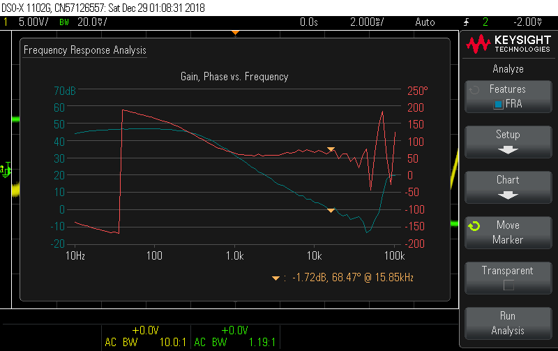
Sophisticated mathematical models are one thing, but useless if you can't validate them. One method to analyze the feedback loop in circuit is by injecting a voltage signal into the feedback line using a function generator and observing how that signal is coupled to the output. My oscilloscope (Keysight 1102-G) has a frequency response analysis tool that produces a Bode chart similar to above by comparing the voltages at both channels as the function generator sweeps through a frequency range. If it works right, the plot will look something like this, taken from an older project.

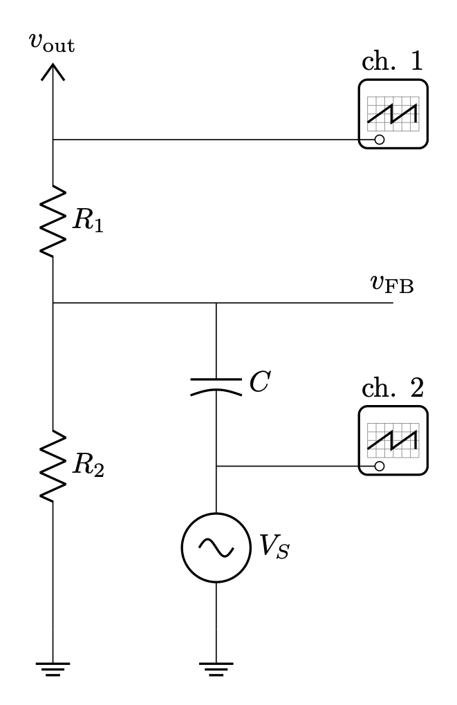
To do this, the signal has to be injected without disturbing the DC value of the feedback line. Here is the sketch of a voltage injection circuit that doesn't break the feedback loop.

At DC, the feedback voltage is just the output voltage scaled by the resistor divider. The capacitor C is large, say 1000 µF, and can be thought of as a short at any frequency above DC. The source generator VS is a typical function generator with 50 Ω impedance. The total impedance of this branch should be small in comparison to R2 (10 kΩ in the design), which means the DC level of FB is unchanged, but the AC component is almost entirely driven by the function generator. Probes connected to the output voltage and the output of the function generator should be tied to the same ground point, and then the frequency response analysis tool can be started. Because of the high gain of the error amplifier in the LM5155, the voltage level required from VS is very small, and can be more precisely set by coupling VS across a 1/1000 resistor divider.
In the board design, a pair of headers allows the attachment of a function generator, labeled J5 and J6 on the board.
Nixie Tube 170 V flyback DC-DC power converter
Design walkthrough and evaluation of a flyback converter from scratch
 James Wilson